
Abstract
Electro-absorption from GeSi heterostructures is receiving growing attention as a high performance optical modulator for short distance optical interconnects. Ge incorporation with Si allows strong modulation mechanism using the Franz–Keldysh effect and the quantum-confined Stark effect from bulk and quantum well structures at telecommunication wavelengths. In this review, we discuss the current state of knowledge and the on-going challenges concerning the development of high performance GeSi electro-absorption modulators. We also provide feasible future prospects concerning this research topic.
Introduction
Optics are considered to be one of the most viable solutions to the performance limitations of electrical interconnection. Optics have now replaced electronic wires for long-haul telecommunication systems [Citation1]. They offer several advantages over electronics in data transmission, including much higher bandwidth and lower energy dissipation [Citation2, Citation3]. Moreover, optics are being increasingly deployed in intermediate distance telecommunication networks, like metropolitan area networks and local-area networks [Citation4]. It has become clear that our unlimited demands for information appear to necessitate the use of optical data transmission in place of electrical wires at an ever shortening communication distance. The bandwidth and energy dissipation restrictions of copper wire make optical networking preferable, from data center to the end users and, probably, to the microprocessor. Nevertheless, this poses a serious challenge to the present optical technologies based on III–V semiconductors or electro-optic materials like LiNbO3. These technologies are unlikely to be adopted economically and reliably for such high volume markets due to small wafer scale and nonstandardized fabrication. Bringing an optical solution to the large scale integration of silicon (Si) and silicon complementary metal–oxide–semiconductor (CMOS) electronics is arguably one of the most promising approaches in allowing high bandwidth optical technology in the mass market. To surmount such challenges, Si-compatible optical components have been heavily developed and studied in academic and industrial laboratories during the past decade in order to obtain effective optical propagation, generation, detection and modulation in/on Si.
Optical modulation
Optical modulation is indispensable in any optical interconnection system. It converts electrical data into the optical domain and can be obtained either by directly modulating a light source or by using an optical modulator. An optical modulator allows much higher data rates and multilevel modulation formats [Citation5]. It can also allow the system to be relatively less expensive and have better temperature stability [Citation6] because a sophisticated light source is not needed and a single light source could be used for different channels with separate optical modulators [Citation7]. For on-chip application, an off-chip light source with an on-chip optical modulator could potentially be preferable due to on-chip heat dissipation and temperature variation issues [Citation8].
Electro-refraction
Electro-refraction is a well-known approach to obtain optical modulation in Si, as proposed and studied by Soref [Citation9] in 1987. Since the first gigahertz (GHz) Mach–Zehnder interferometer (MZI) modulator was reported in silicon by Intel in 2004 [Citation10], silicon MZI modulators have been intensively studied worldwide [Citation5, Citation11]. They play a major role in commercially available silicon photonics-based 100 gigabit optical transceivers, which are aimed for data communication among servers in data centers (www.luxtera.com, www.kotura.com,). However, it appears that Si MZI modulators are not likely to meet the future requirements of off- and on-chip optical interconnects due to the relatively weak free carrier dispersion in Si. Because of the large size and/or high driving voltage, their energy dissipation of around 1–5 pJ bit−1 is two order of magnitudes higher than the 2–50 fJ bit−1 expected for timely and progressive replacement of the electrical interconnection by the optical interconnection for off- or on-chip interconnection [Citation8]. To circumvent the weak free carrier effect of Si, resonance structures or slow light enhancements have been proposed. Demonstrations of compact and relatively low-energy optical modulators based on these two techniques have recently been reported by various research teams. Their recent progress and on-going challenges are discussed by other contributions within this special issue.
Electro-absorption
Electro-absorption is another technique that can be used to modulate light. Compared to electro-refraction, electro-absorption typically allows a more compact and lower driving voltage optical modulator [Citation12, Citation13]. This component employs either the Franz–Keldysh effect (FKE) or the quantum-confined Stark effect (QCSE) in modulating the band gap energy and, hence, absorption coefficients. It typically employs III–V direct band gap semiconductors, which are widely used in nowadays long-haul and intermediate distance telecommunication networks. Nevertheless, the electro-absorption effect in Si can hardly be useful because it is an indirect band gap semiconductor with the global minimum of the conduction band at the Δ valley far from the zone center [Citation14]. As a result, the indirect absorption dominates all of the optical processes, leading to the poor efficiency of optical devices made of Si optical transition. Incorporation of Ge with Si has been suggested as a way to enhance the active optical properties of the Si photonic platform. Ge, a group IV semiconductor like Si, has already been included in today's CMOS chips in order to improve Si electrical properties [Citation15, Citation16]. At room temperature the direct and indirect gap energies of Ge are ∼ 0.8 and ∼ 0.64 eV, respectively [Citation17, Citation18]. Hence, the Ge direct gap energy of 0.8 eV corresponds well to the C band telecommunication wavelength regions, making Ge an ideal candidate to be engineered for active photonic devices. Ge incorporation to obtain optical detection at telecommunication wavelength on Si has been reported since 1984 [Citation19]. In contrast, its use to achieve strong electro-absorption in Si-compatible material systems began to receive serious attention only recently [Citation20]. In this review we will discuss the current state of knowledge and challenges concerning the development of high performance Ge-rich SiGe electro-absorption modulators. We hope that this review can play a part in shaping the current understanding and the possible future prospects concerning this research topic. This paper will first summarize the electro-absorption properties in GeSi. It will then discuss the demonstrated device performance in the second part.
Electro-absorption in Ge-rich SiGe material systems
Electro-absorption mechanisms give optical modulation through changing the bulk material band gap energy according to the applied electric field, which is called the Franz–Keldysh effect (FKE) [Citation21]. An electric field shifts the absorption edge of the material to the longer wavelengths, enhancing the absorption coefficients at the weakly absorbing regime and giving optical modulation as in figure (a), which shows the typical transmission spectra of FKE. The FKE from the direct band gap absorption of bulk Ge dates back to 1965 when it was experimentally demonstrated [Citation22]. Nevertheless, FKE from epitaxial Ge on Si substrate were reported only in 2006 [Citation23]. In 2007, Liu et al [Citation24] proposed that an inclusion of a small amount of Si (0.75%) into Ge will enable significant optical modulation from Ge1−xSix at the telecommunication wavelength of 1.55 μm. It is proposed that epitaxial Ge0.9925Si0.0075 on Si would have a direct band gap transition that is slightly higher than 0.8 eV (1.55 μm). The band gap energy was calculated by taking into account both the addition of 0.75% Si and the additional tensile strain of around 0.2% that is induced in Ge0.9925Si0.0075 after high temperature annealing epitaxial steps due to its thermal expansion coefficient mismatch with Si [Citation25]. Such a low Si content is expected not to significantly degrade the sharp raise of Ge direct gap absorption when working at 1.55 μm [Citation26, Citation27]. An efficient Ge1−xSix optical modulator has been successfully demonstrated by a number of research teams, as discussed in the following part of this paper.
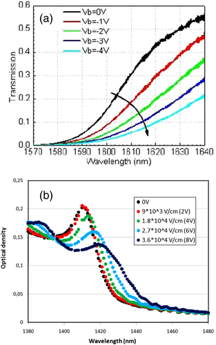
Figure 1 (a) Typical FKE measured from Ge direct gap absorption band edge. (Reproduced with permission from [Citation51] © 2011 the Optical Society.) (b) QCSE measured from Ge/Si0.15Ge0.85 MQWs on Si0.1Ge0.9 relaxed buffer. Two main characteristics of the QCSE are observed: the Stark (red) shift of the absorption spectra and the reduction of the exciton related absorption peak due to the reduction of the overlap between the electron and hole wave functions.
The quantum-confined Stark effect
QCSE or FKE in quantum well structures, is a strong alternative to realize a high performance optical modulator [Citation28]. The interest of using QW structures results from its discrete energy levels thanks to the quantum confinement effect. For optical modulation, this leads to a sharper rise of the absorption edge than in the bulk material; hence, a large variation of absorption coefficients with a relatively small amount of applied electric fields is possible [Citation29]. In Ge, in 2005 Kuo et al [Citation20] from Stanford University reported the breakthrough discovery of strong QCSE around light wavelength of 1.45 μm at room temperature from ten periods of 10 nm thick Ge well sandwiched by 16 nm thick Si0.15Ge0.85 barriers (Ge/Si0.15Ge0.85 multiple quantum wells (MQWs)) on a Si0.1Ge0.9 relaxed buffer directly grown on Si substrate. The absorption edge is shifted from the 1.55 μm (0.8 eV) of bulk Ge due to both the compressive strain induced in Ge QWs with respect to Si0.1Ge0.9 relaxed buffer and the confinement effect in the QWs. The average Ge concentration in Ge/SiGe MQWs is designed to equal that of the Si0.1Ge0.9 relaxed buffer in order to achieve epitaxial growth of high quality thick strain-compensated Ge/SiGe MQWs. The absorption coefficients deduced from photocurrent measurements show strong QCSE from Ge QWs based on Ge direct-gap transition between the first valence band heavy hole (HH) level and the first conduction state at Γ (HH1–cΓ1). QCSE from Ge QWs is reported to be as strong as that from the direct-gap III–V semiconductors due to a strong absorption coefficient of Ge. This discovery was later studied on a similar Ge/Si0.15Ge0.85 MQWs prepared on Si substrate through the use of a high growth rate graded buffer by low-energy plasma-enhanced chemical vapor deposition (LEPECVD) at room and low temperature [Citation30, Citation31]. Modulation performance was investigated from both photocurrent and transmission measurements in [Citation31]. Absorption from Ge/SiGe MQWs with an exciton peak having the lowest reported half-width at half maximum of 6 meV at room temperature was measured as in figure (b). This indicates the good quality of the Ge/SiGe MQWs grown by LEPECVD on a SixGe1−x graded buffer.
Polarization dependence of QCSE from Ge/Si0.15Ge0.85 MQWs
Polarization dependence of QCSE from Ge/Si0.15Ge0.85 MQWs has also been explored theoretically and experimentally [Citation32–Citation36]. Interestingly, using a tight-binding description, Virgilio and Grosso [Citation33] pointed out in 2008 that the direct-gap transition between the first valence band light hole (LH) level and the first conduction state at Γ (LH1–cΓ1) from Ge QWs can have a stronger absorption modulation than that from the conventionally studied HH1–cΓ1 due to QW optical selection rules and the lower band offset of LH band in Ge/SiGe MQWs [Citation37]. It suggested that LH1–cΓ1 absorption and modulation could be significantly enhanced by using transverse-magnetic (TM) polarized light (electric field perpendicular to the QW plan). Only LH related transition is allowed with combined oscillator strength of HH- and LH-related transitions from the case with transverse-electric (TE) polarized light [Citation38]. In 2009, Virgilio et al [Citation34] experimentally showed a reduction of absorption from HH1–cΓ1 transition when the polarization changed from TE to TM using prism-shaped structures; nevertheless, due to the experimental conditions, TM polarized optical absorption was not fully enhanced and QCSE was not reported. In 2013, Chaisakul et al [Citation36] performed photocurrent and transmission spectral measurements on Ge/Si0.15Ge0.85 MQWs to make a comparative study of QCSE from their HH- and LH-related transitions using both TM and TE polarized light. It was demonstrated in [Citation36] that the direct-gap transition of Ge QWs exhibited strong polarization dependence, as strong as the one observed from III–V based QWs. The strong QCSE from LH1–cΓ1 transitions observed from the experiments using TM polarized light suggested that LH1–cΓ1 transitions could be considered in lieu of conventional HH1–cΓ1 transitions to enable a more compact optical modulator by a factor of three with the same level of modulation efficiency.
Ge/SiGe MQWs can be engineered to obtain significant QCSE around the telecommunication wavelength of 1.3 μm
Ge/SiGe MQWs can be engineered to obtain significant QCSE around the telecommunication wavelength of 1.3 μm. This can be achieved by either applying a higher level of compressive strain on Ge QWs, increasing QW quantum confinement energy or enlarging the band gap energy of QWs via Si addition of around 1% [Citation39, Citation40]. In 2011, Lever et al [Citation41] experimentally reported Ge/Si0.4Ge0.6 on a relaxed Si0.22Ge0.78 buffer. The structures successfully produce QCSE around light wavelength of 1.3 μm thanks to larger compressive strain in Ge QWs with respect to Si0.22Ge0.78 relaxed buffer, which is responsible for absorption edge blue shift. Rouifed et al [Citation42] reported on a similar composition of Ge/Si0.35 Ge0.65 on a relaxed Si0.21Ge0.79 buffer in 2012. The modulation performance of Ge/SiGe MQWs when designed to work at shorter wavelengths (e.g. at 1.3 μm) was also worth further discussion. A higher compressive strain increases the energy difference between the bottom of Γ − (local minimum of Ge conduction band at the zone center) and L– (global minimum of Ge conduction band) valley conduction band edges. As a result, the absorption ratio between the direct gap transition at Γ-valley and the background loss of L valley indirect absorption will be reduced. (Absorption at L becomes stronger with respect to Γ.) This could have an impact on the modulation performance in terms of associated modulation depth and optical loss.
QCSE from Ge/SiGe MQWs was also investigated around the telecommunication wavelength of 1.55 μm
QCSE from Ge/SiGe MQWs was also investigated around the telecommunication wavelength of 1.55 μm. Kuo et al [Citation43] in 2006 experimentally studied the effect of a decrease in compressive strain and quantum confinement energy in Ge QWs, as well as the variation of substrate temperature to achieve QCSE at 1.55 μm with Ge/Si0.175Ge0.825 MQWs on a relaxed Si0.05Ge0.95 buffer. The use of Si0.05Ge0.95 relaxed buffer significantly reduced the level of compressive strain applied on Ge QWs, while a relatively thick Ge QWs of 12.5 nm was used to decrease the QW confinement energy. QCSE was successfully demonstrated around 1.55 μm at a substrate temperature of 90 °C, which is comparable to a silicon electronic chip operating environment. It is theoretically predicted that a further reduction of compressive strain in Ge QWs by using a relaxed Si0.025Ge0.975 buffer [Citation39] or an additional decrease in quantum confinement energy in Ge QWs by using a thicker Ge QWs of 14 nm [Citation40] could allow 1.55 μm QCSE operations at room temperature. It is also worth noticing that care should be taken in decreasing the quantum confinement energy of Ge QWs as it could lead to considerable reduction of excitonic absorption and, hence, degrading the sharp rise of absorption edge and modulation performance. In 2011, Ren et al [Citation44] experimentally demonstrated that Ge/Si0.15Ge0.85 MQWs on a Si0.1Ge0.9 relaxed buffer can provide optical modulation from light wavelengths of 1450–1550 nm with an applied electric field of as high as 20 V μm−1. Additionally, application of tensile strain can be used to obtain Ge QWs with direct gap transition around 1.55 μm. Chen et al [Citation45] and Carroll et al [Citation46] prepared tensile-strained Ge/SiGe MQWs through tensile-strained Ge virtual substrate, and showed direct-gap excitonic transition around 1.55 μm from the photoluminescence and transmission spectra at room temperature. To our knowledge, no QCSE has yet been demonstrated from such an approach.
It is worth noting that typically in III–V MQW electro-absorption modulator the absorption saturation due to the field screening effect could limit the maximum input power of the device [Citation47]. Nevertheless, in Ge MQWs the indirect band-gap of Ge could prevent such an effect. Indeed, the photogenerated carriers suffer for rapid intervalley scattering from Γ to L, which occurs in hundreds of femtoseconds [Citation48]. In practice one could expect the maximum input level in Ge MQW electro-absorption modulator to be the power level that induces nonlinearity, such as two-photon absorption or four-wave mixing, as in Si electro-refractive modulators. This nonlinearity power level is normally beyond that required in one-channel telecommunication systems.
GeSi electro-absorption modulator
Significant advances have been made regarding the GeSi FKE optical modulator. Relatively, bulk material is easier to grow and fabricate than QW. To obtain significant optical modulation, an FKE modulator is usually based on waveguide configuration to allow a long interaction length along the propagation axis. Liu et al [Citation49] demonstrated the first GeSi FKE butt-coupled with submicron Si waveguide, as in figure (a). It is shown for the first time that an FKE from GeSi system (0.75% of Si) can provide low energy and fast optical modulation with sufficiently large optical bandwidth around optical wavelength of 1.55 μm. In 2012, Feng et al [Citation50] demonstrated an FKE GeSi (0.7% of Si) optical modulator butt-coupled with a large cross section Si waveguide platform, as in figure (b), which could offer lower fiber coupling loss, waveguide propagation loss, polarization dependent loss and polarization dependent frequency shift compared to the submicron waveguide approach. The modulator exhibited a competitive performance in terms of device footprint, optical bandwidth, modulation depth, insertion loss, bias voltage and modulation bandwidth, as summarized in table . It is also possible to employ bulk Ge for FKE optical modulators with optimum modulation efficiency around 1.6 μm [Citation51–Citation53], which should be discussed along with Ge photodetection by another contribution of this special issue.
Figure 2 Schematic representation of: (a) a GeSi FKE modulator butt-coupled with submicron Si waveguide in [Citation49] showing for the first time that FKE from GeSi system (0.75% of Si) can provide low energy and fast optical modulation with significant optical bandwidth around 1.55 μm; and, (b) a GeSi FKE (0.7% of Si) optical modulator butt-coupled with a large cross section Si waveguide in [Citation50]. The modulator exhibited a competitive performance of device footprint, optical bandwidth, modulation depth, insertion loss, bias voltage, and modulation bandwidth. (Reproduced with permission from [Citation49] © 2008 Nature Publishing Group and [Citation50] © 2012 the Optical Society.)
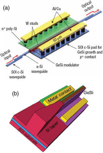
Table 1 Summary of performance matrices obtained from FKE GeSi and QCSE Ge/SiGe MQW optical modulators experimentally reported to date.
QCSE optical modulators
QCSE optical modulators from Ge/SiGe MQWs have been reported in side entry, surface illumination and waveguide configurations, which are summarized with the aforementioned GeSi FKE modulators in table . The experimental characterization results from each QCSE modulator architecture indicate its strong potential to render competitive modulation performance at low voltage due to the strong modulation mechanism of QCSE. In 2007, Roth et al [Citation54] demonstrated Ge/SiGe MQW modulator with a side-entry configuration. Using a side-entry approach to facilitate in- and out-coupling of light with Ge/SiGe MQW modulator on Si chip can potentially relax the alignment constraints with the optical fiber compared to the waveguide architecture. The use of an asymmetric Fabry–Perot resonator formed between the active regions of Ge/SiGe MQWs resulted in adequate values of modulation depth and bandwidth with a reasonable voltage swing. A side-entry design with increasing quality factor of the resonator, as in figure (a), was later reported in [Citation55]. The modulator operating at a driving voltage of 1 V peak-to-peak gave 3 dB modulation contrast around light wavelength of 1.55 μm at 100 °C. A vertical-incidence QCSE optical modulator is also of interest. For the free space approach, the use of an on-chip normal incident modulator instead of VCSEL could be attractive due to its higher thermal stability and lower susceptibility to crystalline defect [Citation8]. The characterization of vertical-incidence QCSE optical modulator was reported in 2010 and high speed performance of 3–10 GHz modulation bandwidth was measured from the tested device with optical input and output facet on the top and bottom side of the wafer, respectively [Citation56]. In 2012, Edwards et al [Citation57] demonstrated vertical-incidence QCSE modulators based on a moderate-Q asymmetric Fabry–Perot cavity formed by distributed Bragg reflector surrounding the Ge/SiGe MQWs, as in figure (b). The structure allows the optical signal to be coupled in and out from the top of the device. An open eye diagram at 2 Gbit s−1 with 3.5 GHz 3 dB modulation bandwidth was measured from a 60 μm diameter tested device, and substantial improvement may be expected by further decreasing device dimensions. In 2011, Chaisakul et al [Citation35] reported a QCSE modulator in a planar waveguide structure from 34 μm long planar waveguide directly coupled with the input fiber. In 2012, the high speed operation of direct fiber-coupled device was reported at 23 GHz from a 3 μm wide and 90 μm long Ge/SiGe MQW waveguide, as in figure (c) [Citation58]. As summarized in table , with a swing voltage of 1 V between 3 and 4 V, an extinction ratio of as high as 9 dB was measured with an estimated dynamic energy consumption of 16 fJ bit−1 around at light wavelength of 1435 nm. With bias voltage of 5 V (∼ 7.5 × 10⁴ V cm−1), 11 dB extinction ratio with 7.5 dB insertion loss can be simultaneously obtained at a bit longer light wavelength of 1440 nm. This result demonstrated that Ge/SiGe MQWs can render the same modulation depth as that of III–V based device [Citation59] at similar device length and electrical bias with an additional optical loss due to Ge indirect-gap absorption as discussed by Schaevitz et al [Citation60] and Kim and Ahn [Citation61] in 2011. To illustrate, at a comparable device footprint and at their optimum operating wavelength, while Ge MQW modulator rendered 11 dB extinction ratio and 7 dB absorption loss with 5 V bias (∼ 7.5 × 10⁴ V cm−1) [Citation58], a direct-gap III–V modulator resulted in 10 dB extinction ratio and 1 dB absorption loss with 4 V bias (∼ 11 × 104 V cm−1) [Citation59]. As a perspective, Lim et al [Citation62] recently proposed the use of an add-drop ring structure to overcome the indirect-gap absorption of silicon–germanium.
Figure 3 Schematic representation of: (a) a side-entry QCSE modulator in [Citation55], showing operation at a driving voltage of 1 V peak-to-peak gave 3 dB modulation contrast around light wavelength of 1.55 μm at 100 °C; (b) a vertical-incidence QCSE optical modulator based on a moderate-Q asymmetric Fabry–Perot cavity formed by distributed Bragg reflector surrounding the Ge/SiGe MQWs proposed for free space interconnection in [Citation57]; and (c) direct fiber-coupled QCSE optical modulator with 23 GHz modulation bandwidth and 9 dB extinction ratio for a swing voltage of 1 V between 3 and 4 V in [Citation58]. (Reproduced with permission from [Citation55] © 2008 The Institution of Engineering and Technology and [Citation57, Citation58] © 2012 the Optical Society.)

Waveguide-integrated QCSE optical modulators
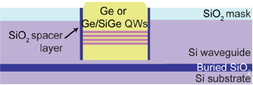
Waveguide-integrated QCSE optical modulators are also important as they enable on-chip integration with other optical functionalities, such as detection, propagation and emission. Efficient waveguide integration of QCSE optical modulators is significant as performance improvement can be expected using QCSE modulator. The experimentally obtained Δα/α (ratio between absorption change and background absorption loss) of Ge QCSE was shown to be as high as 3.6 at its optimum operating wavelength [Citation20], while for bulk GeSi the Δα/α was experimentally reported to be approximately 2, although much improvement can be expected according to the theoretical simulation [Citation50]. In 2012, Ren et al [Citation63] studied butt coupling integration between a submicron Si waveguide and Ge/SiGe MQWs. A Ge/SiGe MQW optical modulator, as in figure , with record device footprint of 8 μm2 was demonstrated with estimated dynamic energy consumption of 0.75 fJ bit−1 [Citation64]. The demonstrator exhibited relatively high coupling loss due to the mode mismatch between the thin Si waveguide core and the thick Ge/SiGe MQWs modulator region. Claussen et al [Citation65] later demonstrated that integration with a large core Si waveguide platform is possible; therefore, a minimized optical coupling loss could be expected in the future. Evanescent coupling is also a promising approach for efficient optical coupling between the Si waveguide and the Ge active layers [Citation66]. The taper section required for adiabatic coupling can be normally long and increases the device footprint. Nevertheless, in 2012 Lever et al [Citation67] proposed a two step taper approach which can significantly reduce taper length compared to the conventional linear taper approach. Although no practical evanescent coupling QCSE modulator has yet been demonstrated, recent optical simulation shows that an efficient waveguide-integrated QCSE modulator can be fabricated based on this concept [Citation68].
Figure 4 Schematic of a butt coupling integration demonstrated in [Citation64, Citation65] between a submicron Si waveguide and QCSE optical modulator. A record device footprint of 8 μm2 was demonstrated with estimated dynamic energy consumption of 0.75 fJ bit−1. (Reprint permission from [Citation65] © 2012 the Optical Society.)
Conclusions
In conclusion, electro-absorption from GeSi on Si is one of the most promising candidates to realize a compact, low-energy, fast, temperature stable and high-volume optical modulator for short distance optical interconnects. High performance optical modulators have been demonstrated by both FKE and QCSE. For waveguide integration, an FKE modulator butt coupled with Si waveguide has been shown with acceptable performance matrix, while efficient integration of QCSE device with input and output waveguide is still under development. Significant progress can be expected within the next few years given the current pace of work. Concerning device performance, it should be noted that the requirements of an optical modulator varies according to applications and the performance matrix of short scale interconnects can be considerably different than those conventionally applied to long-haul or intermediate distance optical communication. For example, it was mentioned that an optical modulator with 5 dB extinction ration with 3 dB insertion loss could be considered suitable for chip scale communication [Citation40], which is significantly lower than 15–20 dB modulation required for long-haul optical networks. On the contrary, energy dissipation is more critical for chip scale interconnects due to the definite limit of power dissipation available on a chip. Although it is not certain which of the competing solutions (resonator, slow light, GeSi) will emerge as the most suitable option for short distance optical communication, all indicate a potential to produce sufficiently strong optical modulation with satisfactory values of related performance matrix. The successful development of an optical modulator that can be integrated seamlessly with CMOS integrated circuits should be one of the keys in overcoming the delay, power and bandwidth limitations of metal interconnects from the data center to the end users, and down to the microprocessor.
Related Research Data
References
- KirchainRKimerlingL 2007 Nature Photon. 1 303 10.1038/nphoton.2007.84
- MillerD A B 1997 Int. J. Optoelectron. 11 155
- MillerD A B 2000 Proc. IEEE 88 728 10.1109/5.867687
- ReedG TKnightsA P 2004 Silicon Photonics: An Introduction New York Wiley
- ReedG TMashanovichG ZGardesF YThomsonD J 2010 Nature Photon. 4 518 10.1038/nphoton.2010.179
- KekatpureR DLentineA 2013 Opt. Express 21 5318 10.1364/OE.21.005318
- De DobbelaereP 2012 Si photonics based high-speed optical transceivers European Conf. and Exhibition on Optical Communication Washington, DC Optical Society of America paper We.1.E.5
- MillerD A B 2009 Proc. IEEE 97 1166 10.1109/JPROC.2009.2014298
- SorefRBennettB 1987 IEEE J. Quantum Electron 23 123 10.1109/JQE.1987.1073206
- LiuAJonesRLiaoLSamara-RubioDRubinDCohenONicolaescuRPanicciaM 2004 Nature 427 615 10.1038/nature02310
- Marris-MoriniD 2009 Proc. IEEE 97 1199 10.1109/JPROC.2009.2015337
- SteinmannPBorchertBStegmullerB 1997 IEEE Photon. Technol. Lett. 9 1561 10.1109/68.643260
- FukanoHYamanakaTTamuraM 2007 J. Light. Technol. 25 1961 10.1109/JLT.2007.901328
- CardonaMPollakF H 1996 Phys. Rev. 142 530 10.1103/PhysRev.142.530
- SchafflerF 1997 Semicond. Sci. Technol. 12 1515 10.1088/0268-1242/12/12/001
- CresslerJ D 1998 IEEE Trans. Microw. Theory Tech. 46 572 10.1109/22.668665
- MacFarlaneG GMcLeanT PQuarringtonJ ERobertsV 1957 Phys. Rev. 108 1377 10.1103/PhysRev.108.1377
- DashW CNewmanR 1955 Phys. Rev. 99 1151 10.1103/PhysRev.99.1151
- LuryiSKastalskyABeanJ C 1984 IEEE Trans. Electron. Dev. ED-31 1135 10.1109/T-ED.1984.21676
- KuoY-HLeeY KGeYRenSRothJ EKaminsT IMillerD A BHarrisJ S 2005 Nature 437 1334 10.1038/nature04204
- KeldyshL V 1957 J. Exp. Theor. Phys. 33 994
- FrovaAHandlerP 1965 Phys. Rev. 137 A1857 10.1103/PhysRev.137.A1857
- JongthammanurakSLiuJWadaKCannonD DDanielsonD TPanDKimerlingL CMichelJ 2006 Appl. Phys. Lett. 89 161115 10.1063/1.2363948
- LiuJPanDJongthammanurakSWadaKKimerlingL CMichelJ 2007 Opt. Express 15 623 10.1364/OE.15.000623
- IshikawaYWadaKCannonD DLiuJLuanH-CKimerlingL C 2003 Appl. Phys. Lett. 82 2044 10.1063/1.1564868
- LuoY 2011 Proc. SPIE 7944 79440P
- BraunsteinRMooreA RHermanF 1958 Phys. Rev. 109 695 10.1103/PhysRev.109.695
- MillerD A BChemlaD SDamenT CGossardA CWiegmannWWoodT HBurrusC A 1984 Phys. Rev. Lett. 53 2173 10.1103/PhysRevLett.53.2173
- MillerD A BChemlaD SDamenT CGossardA CWiegmannWWoodT HBurrusC A 1985 Phys. Rev. B 32 1043 10.1103/PhysRevB.32.1043
- TsujinoSSiggHMusslerGChrastinaDVon KänelH 2006 Appl. Phys. Lett. 89 262119 10.1063/1.2425032
- ChaisakulPMarris-MoriniDIsellaGChrastinaDLe RouxXGattiEEdmondSOsmondJCassanEVivienL 2010 Opt. Lett. 35 2913 10.1364/OL.35.002913
- PaulD J 2008 Phys. Rev. B 77 155323 10.1103/PhysRevB.77.155323
- VirgilioMGrossoG 2008 Phys. Rev. B 77 165315 10.1103/PhysRevB.77.165315
- VirgilioMBonfantiMChrastinaDNeelsAIsellaGGrilliEGuzziMGrossoGSiggHvon KänelH 2009 Phys. Rev. B 79 075323 10.1103/PhysRevB.79.075323
- ChaisakulPMarris-MoriniDIsellaGChrastinaDLe RouxXEdmondSCassanEVivienL 2011 Opt. Lett. 36 1794 10.1364/OL.36.001794
- ChaisakulP 2013 Appl. Phys. Lett. 102 191107 10.1063/1.4805004
- SchaevitzR KRothJ ERenSFidanerOMillerD A B 2008 IEEE J. Sel. Top. Quantum Electron. 14 1082 10.1109/JSTQE.2008.918935
- BastardG 1988 Wave Mechanics Applied to Semiconductor Heterostructures Les Ulis Les Editions de Physique
- LeverLIkonicZValavanisACooperJKelsallR 2010 J. Light. Technol. 28 3273
- SchaevitzR KEdwardsE HRothJ EFeiE TRongYWahlPKaminsT IHarrisJ SMillerD A B 2012 IEEE J. Quantum Electron. 48 187 10.1109/JQE.2011.2170961
- LeverL 2011 Opt. Lett. 36 4158 10.1364/OL.36.004158
- RouifedM SChaisakulPMarris-MoriniDFrigerioJIsellaGChrastinaDEdmondSLe RouxXCoudevylleJ-RVivienL 2012 Opt. Lett. 37 3960 10.1364/OL.37.003960
- KuoY-HLeeY KGeYRenSRothJ EKaminsT IMillerD A BHarrisJ S 2006 IEEE J. Sel. Top. Quantum Electron. 12 1503 10.1109/JSTQE.2006.883146
- RenSRongYKaminsT IHarrisJ SMillerD A B 2011 Appl. Phys. Lett. 98 151108 10.1063/1.3574912
- ChenYLiCLaiHChenS 2010 Nanotechnology 21 115207 10.1088/0957-4484/21/11/115207
- CarrollLImbertFSiggHSüessMMüllerEVirgilioMPizziGRossbachPChrastinaDIsellaG 2011 Appl. Phys. Lett. 99 031907 10.1063/1.3606383
- WeinerJ SChemlaD SMillerD A BHausH AGossard A CWiegmannWBurrusC A 1985 Appl. Phys. Lett. 47 664 10.1063/1.96051
- ClaussenS ATasyurekERothJ EMillerD A B 2010 Opt. Express 18 25596 10.1364/OE.18.025596
- LiuJBealsMPomereneABernardisSSunRChengJKimerlingL CMichelJ 2008 Nature Photon. 2 433 10.1038/nphoton.2008.99
- FengD 2012 Opt. Express 20 22224 10.1364/OE.20.022224
- FengN-N 2011 Opt. Express 19 7062 10.1364/OE.19.007062
- LimA E-JLiowT-YQingFDuanNDingLYuMLoG-QKwongD-L 2011 Opt. Express 19 5040 10.1364/OE.19.005040
- SchmidMKaschelMGollhoferMOehmeMWernerJKasperESchulzeJ 2012 Thin Solid Films 525 110 10.1016/j.tsf.2012.10.087
- RothJ EFidanerOSchaevitzR KKuoY-HKaminsT IHarrisJ SMillerD A B 2007 Opt. Express 15 5851 10.1364/OE.15.005851
- RothJ EFidanerOEnglundE ESchaevitzR KKuoY-HHelmanN CKaminsT IHarrisJ SMillerD A B 2008 Electron. Lett. 44 49 10.1049/el:20082979
- RongYGeYHuoYFiorentinoMTanM R TKaminsT IOchalskiT JHuyetGHarrisJ S 2010 IEEE J. Sel. Top. Quantum Electron. 16 85 10.1109/JSTQE.2009.2031502
- EdwardsE HAudetR MFeiE TClaussenS ASchaevitzR KTasyurekERongYKaminsT IHarrisJ SMillerD A B 2012 Opt. Express 20 29164 10.1364/OE.20.029164
- ChaisakulPMarris-MoriniDRouifedM-SIsellaGChrastinaDFrigerioJLe RouxXEdmondSCoudevylleJ-RVivienL 2012 Opt. Express 20 3219 10.1364/OE.20.003219
- KuoY-HChenH-WBowersJ E 2008 Opt. Express 16 9936 10.1364/OE.16.009936
- SchaevitzR KLy-GagnonD SRothJ EEdwardsE HMillerD A B 2011 AIP Adv. 1 032164 10.1063/1.3646149
- KimJAhnD 2011 J. Appl. Phys. 110 083119 10.1063/1.3656688
- LimP HCaiJIshikawaYWadaK 2012 Opt. Lett. 37 1496 10.1364/OL.37.001496
- RenSKaminsT IMillerD A B 2011 IEEE Photon. J. 3 739 10.1109/JPHOT.2011.2162644
- RenSRongYClaussenS ASchaevitzR KKaminsT IHarrisJ SMillerD A B 2012 IEEE Photon. Technol. Lett. 24 461 10.1109/LPT.2011.2181496
- ClaussenS ABalramK CFeiE TKaminsT IHarrisJ SMillerD A B 2012 Opt. Mater. Express 2 1336 10.1364/OME.2.001336
- AhnDKimerlingL CMichelJ 2011 J. Appl. Phys. 110 083115 10.1063/1.3642943
- LeverLIkonićZKelsallR W 2012 Opt. Express 20 29500 10.1364/OE.20.029500
- EdwardsE HLeverLFeiE TKaminsT IIkonicZHarrisJ SKelsallR WMillerD A B 2013 Opt. Express 21 867 10.1364/OE.21.000867