
Abstract
In this article, we review our recent work on mid-infrared (mid-IR) photonic materials and devices fabricated on silicon for on-chip sensing applications. Pedestal waveguides based on silicon are demonstrated as broadband mid-IR sensors. Our low-loss mid-IR directional couplers demonstrated in SiNx waveguides are useful in differential sensing applications. Photonic crystal cavities and microdisk resonators based on chalcogenide glasses for high sensitivity are also demonstrated as effective mid-IR sensors. Polymer-based functionalization layers, to enhance the sensitivity and selectivity of our sensor devices, are also presented. We discuss the design of mid-IR chalcogenide waveguides integrated with polycrystalline PbTe detectors on a monolithic silicon platform for optical sensing, wherein the use of a low-index spacer layer enables the evanescent coupling of mid-IR light from the waveguides to the detector. Finally, we show the successful fabrication processing of our first prototype mid-IR waveguide-integrated detectors.
Introduction
Integrated, on-chip photonic devices present a compelling solution to several technical challenges due to their small footprint, low fabrication cost and immunity to electromagnetic interference. Their versatility is showcased by applications that range from high-speed telecommunications to on-chip optical interconnects to imaging and photovoltaics. More importantly, integrated photonics is also poised to play a prime role in the emerging field of on-chip biological and chemical sensing. Changes in the real and imaginary parts of the complex refractive index can be used to rapidly detect the presence of biological and chemical species with high sensitivity. In particular, the mid-infrared (IR) wave band (2.5–10 μm) represents a strategically important spectral regime for photonic sensing applications, as characteristic absorption fingerprints of most molecules reside here.
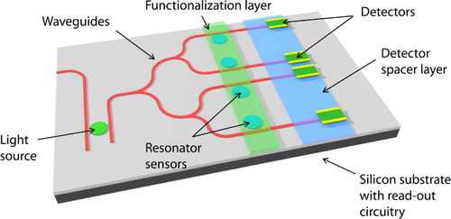
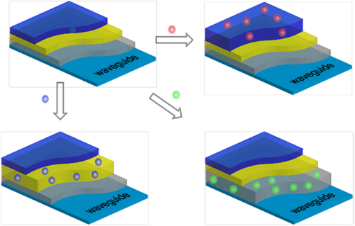
Figure shows a generic schematic illustration of the mid-IR lab-on-a-chip sensor system we envision. The sensor consists of the following basic components: a light source, multiple sensor elements (with or without functionalization layers for specificity), photodetectors and read-out circuitry on a silicon platform. By integrating all the necessary components for mid-IR sensing on a silicon platform, this lab-on-a-chip design enables low-cost and high-sensitivity detection with a small footprint that can lead to its use in remotely deployable arrays of integrated mid-IR sensor devices. In this paper, we focus on the progress we have made on three key individual components—passive waveguides and optical resonators as the sensing element, surface functionalization layers and photodetectors—as well as our efforts toward integrating them on a monolithic silicon platform.
Figure 1. Schematic of a mid-IR lab-on-a-chip sensor system that combines a light source, sensing elements, a detector and read-out circuitry on a monolithic silicon platform. The functionalization layer adds specificity to the sensor response for greater accuracy in analyte recognition (image courtesy of [Citation33]).
Waveguides and micro-resonators for sensing
At the component level, passive waveguides and optical resonators constitute the key sensing elements for mid-IR spectroscopy. Waveguide sensors can transmit a wider wavelength range and hence are useful for finger-printing across the entire mid-IR region. Resonator sensors with a large quality (Q) factor can offer very high sensitivity to changes in the complex refractive index [Citation1–Citation4]. The long optical path length in a resonant cavity leads to higher sensitivity from enhanced photon–matter interactions due to spatial light confinement over a longer period of time. In addition, it is feasible to fabricate resonator arrays that can be used for parallelized detection of multiple species while maintaining a small footprint.
A diverse range of material systems has been explored for passive mid-IR waveguide and resonator fabrication. In addition to silicon-on-insulator (SOI) devices operating at up to 4.4 μm [Citation5–Citation8], the examples include suspended silicon [Citation9, Citation10], silicon on sapphire [Citation11–Citation13], III–V semiconductors [Citation14, Citation15], silicon on porous silicon [Citation16], silver halides [Citation17] and non-oxide glasses [Citation18, Citation19]. We note that the material selection criteria for passive mid-IR photonic applications may be vastly different from the conventional standards we take for granted in optimizing near-IR materials operating in the telecommunication bands. For example, SOI and silica-on-silicon have been the dominant material platforms for integrated photonic devices operating in the near-IR region. However, their transmission window in the mid-IR is limited to about 4.5 μm due to the onset of phonon absorption in silica (the absorption coefficient of fused silica glass is ∼40 dB cm−1 at 4.5 μm [Citation20]). In addition, while processing compatibility with mature complementary metal oxide semiconductor (CMOS) manufacturing has often been considered a major advantage, the benefits of CMOS compatibility are largely compromised for mid-IR photonics. Our argument is based on several distinctive features of mid-IR photonics versus its near-IR counterpart. Firstly, applications of integrated mid-IR photonics mostly focus on fragmented niche market needs, which negate the potential cost benefits associated with high-volume CMOS production [Citation21]. Secondly, unlike near-IR devices, which can readily leverage mature CMOS material platforms and fabrication process flows, mid-IR (> 4.5 μm) photonic device fabrication often necessitates specialized processing steps (e.g. thick cladding layer deposition or deep undercut etching to isolate guided modes from silicon dioxide), which largely prohibits the use of shuttle runs sharing CMOS foundry infrastructures [Citation22]. The much larger feature size of mid-IR devices also relieves the fabrication tolerance requirement as well as the dependence on state-of-the-art CMOS foundry lines. Last but not least, most mid-IR light sources, such as quantum cascade lasers, have been demonstrated on non-silicon platforms to date [Citation23, Citation24]. Therefore, instead of emphasizing the compatibility with standard CMOS processes, we argue that performance-driven material optimization and the versatility of material/device processing to meet highly diverse end-user application-needs are likely to be among the key requirements for mid-IR photonic materials and systems development.
In addition to silicon (transparent up to 7 μm wavelengths), the dominant material for micro-electronics and integrated photonics, amorphous materials such as silicon nitride [Citation25, Citation26] and non-silicate glasses, including transition metal oxides [Citation27] and chalcogenides [Citation28, Citation29], offer unique performance and processing advantages for passive mid-IR photonics. These materials have reduced phonon energy compared to silica and thus possess broad transmission windows in the mid-IR. Silicon nitride and transition metal oxides typically are transparent from the visible to about 7 μm wavelength and tellurium-based chalcogenide glasses are known to exhibit optical transparency up to 25 μm wavelength [Citation30]. A very low optical attenuation (< 0.1 dB m−1) in the glass materials has been theoretically established [Citation31] and experimentally validated through optical fiber measurements [Citation19]. Unlike crystalline materials with narrowly defined stoichiometry, amorphous compounds, in particular chalcogenides and some transition metal oxides (e.g. TiO2–ZrO2 [Citation27]), have a large capacity for composition alloying without sacrificing their structural stability. The wide range of property tuning is critical for mid-IR applications: for example, mid-IR transparent core and cladding layers with high index contrast (Δn > 1) can be realized in a single amorphous alloy system, which significantly facilitates photonic integration. Most importantly, the amorphous nature and low deposition temperature of these materials allows monolithic deposition on virtually any substrates free of lattice-matching constraints, which enables a wide cross-section of applications including mid-IR laser source integration [Citation19].
Our research efforts thus far have focused on three specially tailored material system choices for passive mid-IR photonics: Si pedestal waveguides, silicon nitride directional couplers and chalcogenide glass resonator devices. These material systems claim the aforementioned processing benefits and desired optical properties for mid-IR sensing applications, and offer distinctive material characteristics and performance advantages to accommodate the diverse needs for different spectroscopic sensing applications.
Novel waveguide designs to adapt crystalline silicon waveguides for sensing beyond 4.5 μm
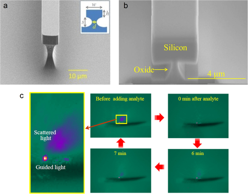
Waveguide-based sensors offer an opportunity for tunable evanescent field sensing. By measuring the attenuation introduced by an absorbing analyte placed in contact with a low-loss waveguide, it is possible to perform sensing measurements over a wider range in the mid-IR. We have recently demonstrated mid-IR waveguide sensors operating at wavelengths from 2.5 to 3.7 μm using pedestal waveguides fabricated from crystalline silicon (shown in figure (a)) [Citation32] that circumvent the SiO2 absorption in the mid-IR (> 4.5 μm). Figure (c) demonstrates the in situ sensing effect (with analyte addition) captured by an InSb camera placed near the output facet of a silicon pedestal waveguide. Prior to analyte addition, the camera image shows a single spot of light from the guided waveguide mode along with some scattered light. Following the chronological sequence as depicted by the thick red arrows in the figure, we see that the scattered light slowly disappears while the guided light intensity is attenuated by the absorption of analyte. The diminished scattered light intensity and the attenuated guided mode gradually recover over time as the analyte starts to evaporate, and they finally return to their original intensity when the analyte has completely evaporated. We have also developed a similar structure on SOI with the pedestal being etched from the silicon dioxide undercladding. These silicon on oxide undercladding pedestal (SOUP) waveguides are shown in figure (b) [Citation33]. The large refractive index contrast and oxide undercut ensure a minimal overlap of the waveguide mode with the silicon dioxide undercladding, and we observe the propagation of mid-IR light at wavelengths up to 3.7 μm.
Figure 2. (a) SEM image of a silicon pedestal waveguide ([Citation32] reproduced by permission of The Royal Society of Chemistry); (b) scanning electron microscope (SEM) image of a SOUP waveguide (image courtesy of [Citation33]) and (c) mid-IR camera images showing the in situ attenuation and recovery of the waveguide mode as an absorbing analyte is introduced and then allowed to evaporate.
The propagation loss in our air-clad pedestal Si structures is measured to be 2.7 ± 0.15 dB cm−1 using paper-clip structures [Citation34]. Since the devices and the substrate come from the same crystalline silicon wafer, our devices exhibit good mechanical stability and no defects are found during the cleaving process. From the mode characterization, the waveguides show a fundamental mode-dominated profile at 3.7 μm. The large dimensions of the waveguide increase the available interaction volume between the probe light and analytes, which increases the sensitivity despite a small evanescent field.
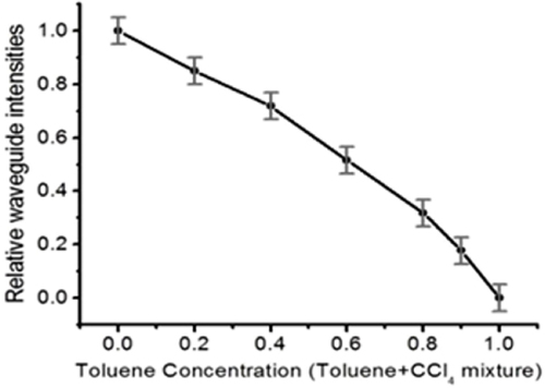
To demonstrate quantitative chemical sensing, air-clad Si pedestal waveguides are used to evaluate organic mixtures with different concentrations of target analytes. Figure shows a plot of toluene (diluted with carbon tetrachloride) concentration versus waveguide mode intensity. As the weight ratio of toluene (CCl4) is gradually increased from 0 to 1, the guided mode light intensity measured at the output end of the waveguide consistently decreases. Since toluene has a strong absorption from the aromatic C–H stretch at λ = 3.3 μm, this is the selected wavelength. Carbon tetrachloride is chosen as the diluent, since it has no C–H bonds, hence its absorption will not interfere with that from toluene.
Figure 3. The waveguide mode intensities at different toluene/CCl4 concentrations. The intensities decrease as the toluene ratio increases because of mid-IR absorption from the aromatic C–H stretch in toluene at the selected wavelength λ = 3.3 μm ([Citation32] reproduced by permission of The Royal Society of Chemistry).
Additionally, we can use the pedestal silicon waveguide structure to identify the chemical make-up of an unknown solution by the appropriate selection of probe wavelengths that overlap with known characteristic absorption features. Silicon's mid-IR transparency window of up to 7 μm allows broadband laser scanning for multi-spectral and diverse chemical analyses. For instance, hexane has a distinguishably higher absorbance at λ = 3.55 μm, whilst compounds containing an amine functional group show an absorption feature between λ = 2.85 and 3.22 μm arising from N–H stretching. Figure shows the measured absorbance for each chosen chemical analyte and compares it with prior literature results [Citation32].
Figure 4. Chemical sensing using our fabricated on-chip mid-IR pedestal silicon waveguide sensor. Tested analytes show different absorbance at λ = 3.55 μm. Results from our measurements (red bars) are compared with those from literature (black bars) ([Citation32] reproduced by permission of The Royal Society of Chemistry).

Design, fabrication and characterization of mid-IR directional couplers in SiN materials
Amorphous low-stress silicon nitride (SiNx) is an excellent material of choice for mid-IR microphotonic sensing devices since it is transparent up to a wavelength of 8.5 μm. Directional coupler devices allow on-chip light manipulation, a desirable feature in differential sensing. To demonstrate such a component for the mid-IR regime, we designed and fabricated SiNx directional couplers operating over the wavelength range 2.45 and 2.65 μm [Citation35]. The spectral response of the fabricated devices, as captured by our mid-IR camera, is shown in figure (a). At an input wavelength of λ = 2.45 μm, a strong guided mode appears in the left waveguide (channel 1) but only a dim signal is observed in the right waveguide (channel 2). As the wavelength increases, the intensity of the left guided mode gradually decreases whereas the light from the right output increases. At λ = 2.55 μm, the power transmitted through both channels is equal (50–50 power splitter). At λ = 2.65 μm, the guided light has completely transitioned into the right arm of our directional coupler.
Figure 5. (a) Captured mid-IR images and (b) intensity profiles of a SiNx directional coupler as a function of wavelength. At λ = 2.45 μm, channel 1 has maximum output, whereas the maximum of channel 2 appears at λ = 2.65 μm. Guided waves remain fundamental modes in both channels. Copyright Wiley-VCH Verlag GmbH & Co. KGaA. Reproduced with permission from [Citation35].
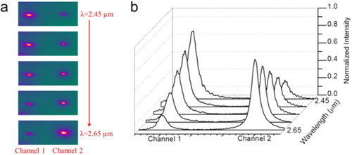
To quantitatively analyze the spectral dependence of the coupling, intensity profiles as a function of wavelength are shown in figure (b). We note that the guided modes from both channels retain sharp Gaussian profiles over the entire spectrum, confirming that the fundamental modes are well preserved during coupling. This preservation of the fundamental mode is critical for many applications, including mid-IR sensing and nonlinear light generation, because a higher-order mode is associated with a different effective refractive index, leading to undesired dispersion which can (a) lead to a false positive sensor signal during mid-IR detection and (b) lower the efficiency of light generation. In addition, the total power from two channels remains constant during coupling yielding a high switching/splitting efficiency with minimal optical loss, thus enabling our SiNx mid-IR platform to be used for real-time on-site toxin monitoring and multi-chemical tracing.
Fabrication and characterization of mid-IR chalcogenide glass resonant cavity devices
Our team has synthesized and characterized a broad range of chalcogenide glass alloys in both bulk and thin-film forms with properties such as glass composition, doping and thermal treatment protocols, all custom-tailored to meet application-specific needs [Citation36–Citation47]. Specific to the IR spectroscopic sensing applications we discuss in this paper, selected chalcogenide glasses possess a photothermal figure- of-merit 100 times higher than those of silica and silicon, making them ideal material candidates for ultra-sensitive photothermal spectroscopic sensing applications [Citation48, Citation49]. We have demonstrated two types of mid-IR resonant cavity devices based on chalcogenide glasses as the basic building blocks for spectroscopic sensors: glass-on-silicon microdisk resonators [Citation49] and waveguide photonic crystal (PhC) cavities [Citation50]. In this section, we will outline the fabrication procedures and optical characterization results at 5.2 μm mid-IR wavelength.
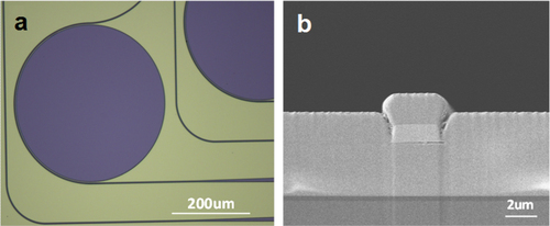
The microdisk resonators were fabricated on 3-inch silicon wafers topped with 300 nm thermal oxide as the starting substrate. A 3 μm-thick Ge23Sb7S70 glass film (n ∼ 2.1) was first deposited as the bottom cladding to prevent absorption in silica and optical leakage into the silicon substrate [Citation51]. Details of the glass synthesis and deposition processes can be found in [Citation51, Citation52]. A 1.1 μm-thick As2Se3 film was subsequently deposited and patterned using photo-resist lift-off to serve as the waveguide core layer. As a final step, a 2 μm-thick Ge23Sb7S70 over-coating layer was deposited on top of the As2Se3 core to prevent the formation of AsOx crystallites due to surface oxidation [Citation53]. The wafers were subsequently cleaved to form end facets for optical coupling into and out of the bus waveguides. Figure (a) shows a top-view optical microscope image of the resonators and figure (b) shows a SEM cross-sectional image of a single-mode bus waveguide.
Figure 6. (a) Optical microscope image of a mid-IR microdisk resonator and (b) SEM cross-section of a single-mode mid-IR bus waveguide (images courtesy of [Citation49]).
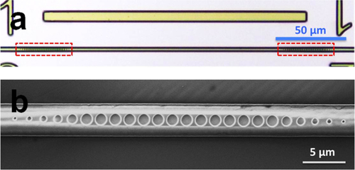
While the Ge23Sb7S70–As2Se3 double layer structure was used for microdisk resonator processing, we chose to fabricate the waveguide PhC cavity on mid-IR transparent CaF2 substrates, given its low refractive index (n = 1.4) critical to Bloch mode confinement in PhCs. The PhC microbeam was fabricated using a two-step process combining lift-off and focused ion-beam (FIB) milling. Instead of sculpting the entire structure using FIB, the two-step process minimizes the milling area and improves throughput. After the fabrication of 3 μm width, 1.2 μm-thick single mode waveguides using UV lithography and lift-off, a layer of 20 nm-thick water-soluble conducting polymer (EspacerTM, Showa Denko) was spin-coated onto the substrate to minimize charge accumulation during ion-beam milling [Citation54]. The PhC holes were drilled using a Ga2+ ion beam (beam current 20 pA, accelerating voltage 30 kV) on a Zeiss Auriga 60 CrossBeamTM FIB nanoprototyping workstation. After milling, the devices were rinsed in deionized water to remove the Espacer layer. The resulting Fabry–Pérot resonant cavity structure consisted of a segment of glass waveguide sandwiched between two identical PhC mirror reflectors. Figure (a) presents an optical microscope top-view image of the cavity and figure (b) shows a SEM top view of a PhC mirror.
Figure 7. (a) Top view microscope image of the waveguide PhC cavity, consisting of a section of unstructured channel waveguide (∼ 170 μm in length) confined between two PhC mirrors (marked by the red boxes) and (b) top-view SEM image of one of the PhC mirrors (images courtesy of [Citation50]).
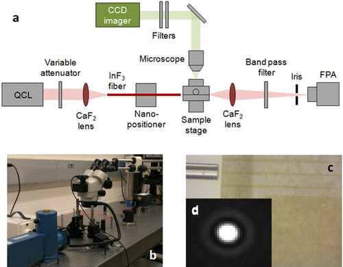
Mid-IR transmission characteristics of the resonant cavity devices were tested using a fiber end fire coupling approach. Figures (a) and (b) show a schematic diagram and a photo of the mid-IR measurement setup. A mid-IR wire-grid polarizer was used to ascertain that the output light from the fiber was transverse electric (TE) polarized. To minimize the coupling loss due to the mode mismatch between the input fiber and the waveguide, an adiabatic lateral taper section was inserted near the input facet, as shown in figure (c). Figure (d) shows the far-field image of the guided mode output from the single mode Ge23Sb7S70 waveguide.
Figure 8. (a) Schematic diagram of the mid-IR fiber-end fire measurement setup (image courtesy of [Citation49]); (b) photo of mid-IR measurement set up; (c) top-view microscope image of a mid-IR InF3 fiber-end fire coupled to an Ge23Sb7S70 waveguide with a lateral taper to reduce the mode mismatch and (d) far-field image of the TE guided mode from a single-mode Ge23Sb7S70 waveguide on the CaF2 substrate.
We employed the cut-back method to determine the propagation loss of waveguides, by sequentially cleaving a waveguide chip into different lengths. We performed the measurements on a minimum of five waveguides for each width, and the average loss values are presented in figure (a). An average optical loss of 4 dB cm−1 was measured in single-mode chalcogenide glass (ChG) bus waveguides. Figure (b) shows the transmission spectrum of the microdisk resonator. The group index calculated from the free spectral range (FSR) is 2.63, which agrees well with our finite difference simulation result (2.68) assuming a fundamental transverse mode order. Figure (c) shows the spectrum measured from the device near its resonance peak at 5157.9 nm wavelength. A loaded Q factor of 105 was inferred from the spectrum, corresponding to an intrinsic Q factor of 2 × 10⁵ and an equivalent waveguide propagation loss of 0.7 dB cm−1. This number is much lower compared to the 4 dB cm−1 loss figure in the bus waveguides, largely due to the reduced interactions of optical modes with the sidewalls in a microdisk whispering gallery mode. This Q factor is among the highest values reported in experimentally demonstrated mid-IR resonators.
Figure 9. (a) Relative output intensity as functions of As2Se3 waveguide lengths; the widths of the waveguides are labeled in the box in the top-right corner; (b) the mid-IR optical transmission spectrum of the As2Se3 microdisk resonator measured using a wavelength sweeping method and (c) the spectrum near the optical resonance at 5157.89 nm wavelength (the red box in (b)). The dots are experimentally measured data and the line is the linear-scale Lorentzian fit, which indicates a loaded cavity quality factor of 105 (images courtesy of [Citation49]).
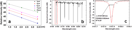
Figure (a) plots the transmission spectrum of a PhC cavity with ten-hole mirror sets. Figure (b) compares the experimentally measured and numerically simulated quality factors as the PhC mirror hole number is varied. The measured Q-factors were averaged from at least seven resonance peaks near the center of the photonic stop band. The figure shows a monotonic increase of the loaded cavity Q-factor as the mirror hole number increases, which is an anticipated result since the external Q-factor scales with the cavity mirror strength. The waveguide loss (53 ± 4 dB cm−1) was first fitted from the measured Q-factors and extinction ratios of the five devices. The high optical loss, which accounts for the relatively low cavity Q, was attributed to gallium ion contamination from FIB milling, as cut-back measurements on unstructured waveguides yielded a much lower propagation loss (figure (a)). Further improvement of the waveguide PhC cavity Q-factors is expected through processing optimization, for example, replacing FIB milling with electron beam lithography patterning [Citation55, Citation56].
Figure 10. (a) The mid-IR transmission spectrum of a waveguide PhC cavity with two ten-hole PhC mirrors and (b) the evolution of loaded cavity Q-factors as the PhC mirror hole number increases: the black bars represent experimentally measured Q values and the red crosses denote the simulation results (images courtesy of [Citation50]).

On-chip cavity-enhanced mid-IR absorption spectroscopy
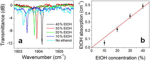
The on-chip cavity-enhanced sensing experiment was implemented using chalcogenide glass microdisk resonators. The operating principles of on-chip cavity-enhanced absorption spectroscopy are discussed in [Citation54, Citation57]. The organic chemicals used in the sensing tests, cyclohexane and ethanol (> 99.5%), were purchased from Sigma-Aldrich. Cyclohexane shows low optical absorption around 5.2 μm and thus was used as the blank solvent. Ethanol has a weak absorption peak (peak absorption ∼ 200 dB cm−1) at 5190 nm wavelength, and was used as the solute for analyzing the performance characteristics of our resonator sensor. Their mixtures were prepared based on volume ratios. During the test, the entire surface area of the mid-IR resonator sensors was covered by drop-cast solutions. Replacing the air with cyclohexane led to an increased coupling strength between the bus waveguide and resonator and a higher extinction ratio, suggesting that the device operates in an under-coupling regime in air. At the same time, the FSR of the resonator changed from 8.23 to 7.81 nm, which corresponded to the group index change from 2.12 to 2.20. The resonator Q-factor, however, remained almost constant, indicating the relatively good optical transparency of cyclohexane at this wavelength range. Each transmission spectrum was obtained by averaging over five wavelength-sweeping scans. The temperature was stabilized at 20 °C throughout the tests.
Figure (a) shows the transmission spectra of the mid-IR Ge23Sb7S70 resonator in cyclohexane solutions of ethanol of different concentrations (given in volume fractions). From the spectra we can see that the extinction ratio decreased with the increasing ethanol concentration, a clear indication of the resonator's transition into the under-coupling regime. The wavelength blue shift of resonance peaks in solutions of different concentrations was attributed to the reduced refractive index of ethanol compared to cyclohexane, from which we estimate a confinement factor of about 10% in the solution. Figure (b) plots the optical absorption induced by ethanol solutions extracted from the spectra in figure (a). While this proof-of-concept experiment demonstrated the feasibility of on-chip cavity-enhanced sensing using chalcogenide glass micro-resonators, the detection limit of the resonator device in terms of the absorption coefficient is estimated to be only ∼0.02 cm−1, corresponding to a tens of parts-per-million level limit of detection when applied to chemical sensing. The sensitivity of the device is primarily limited by the relatively high propagation loss in the resonator (∼ dB cm−1) and can be improved by implementing post-fabrication loss reduction treatment [Citation58] or by resorting to new detection mechanisms that circumvent the intrinsic sensitivity limit of direct cavity-enhanced spectroscopy [Citation48, Citation59].
Figure 11. (a) The mid-IR optical transmission spectrum of a 250 μm radius Ge23Sb7S70 microdisk resonator in an ethanol/cyclohexane mixture of different volume ratios and (b) the absorption loss induced by ethanol calculated from the transmission spectra.
Sensor functionalization for enhanced specificity
Although micro-resonators can be extremely sensitive to variations in the complex refractive index brought about by the presence of very small quantities of an analyte of interest, a good sensor must also be specific, i.e. be able to differentiate between analytes. One way to increase specificity is to coat the top surface of the resonator with a functionalizing layer. Such a layer allows selective adsorption of the species of interest, causing a change in the complex refractive index. Additionally, this layer can be designed to serve as a pre-concentrator with a large partition ratio to the target species. In this section, we describe not only the use of a single polymer film (section 3.1), but we also discuss two new approaches to functionalize sensor surfaces with enrichment polymer layers (EPLs) (multi-layer polymer films in section 3.2 and polymer nanofoams in section 3.3) to enhance sensor pre-concentration and specificity.
Enrichment polymer layers
To enhance the sensitivity of our sensor devices, we have developed a procedure to modify their surfaces with EPLs grafted to their surface [Citation60–Citation67]. EPLs are thin polymer films ( 5 μm) deposited onto a surface, intended to extend the qualitative or quantitative limit of detection by attracting organic compounds via chemical and/or physical interactions. The incorporation of such films into chemical sensors has been heavily researched since the late 1980s [Citation68, Citation69]. EPLs have been demonstrated as efficient and highly sensitive coatings for diverse evanescent waveguide-based optical monitoring systems [Citation70–Citation76]. On exposure to specific analytes, the polymeric coatings will change their internal structure reversibly or irreversibly at the nano-level by swelling with an analyte.
Many different polymer materials have been compared to determine the most effective enrichment layer for specific analytes [Citation70, Citation77, Citation78]. The optical properties of polymer film swelling versus film thickness have also been studied [Citation79]. Large offsets of non-absorbing wavelengths observed in optical chemical sensors are due to the refractive index changes of the absorbing compound. This indicates that the waveguide is evanescently coupled to the sensing medium, even if there is no absorption. To reduce the refractive index changes that result from the incorporation of analyte, it has been suggested that a thin polymer film (< 0.5 μm) is sufficient to avoid interferences from swelling.
Multilayered nanostructured polymer films as EPLs
The necessity of a specific, often unique, coating creates a major stumbling block for the universality of infrared attenuated total reflectance (IR-ATR) based sensors. When a substance with an unknown chemical composition is present in an environment, the use of a number of polymers of dissimilar chemical nature in a single EPL increases the probability of capturing the molecules for detection and analysis. To this end, we developed an enrichment polymer film capable of concentrating chemical substances of different natures at IR-ATR waveguide surfaces (including optical resonators) [Citation60]. Specifically, multilayered nanostructured polymer films chemically grafted to the surface of the IR-ATR waveguide were fabricated as shown in figure .
Figure 12. Scheme of layered polymers on waveguides where each layer has an affinity to a particular organic molecule or compound ([Citation60] reproduced by permission of The Royal Society of Chemistry).
The grafted EPLs, with a total thickness of ∼25–35 nm, consist of five or six polymer layers. The macromolecules constituting the layers were chosen based on the following principles: (a) immiscibility, to guarantee the individuality of each layer; (b) chemical composition, to guarantee that each layer is capable of attracting substances of a different nature and (c) complementary chemical reactivity, to guarantee that every consecutive top layer is chemically anchored to the bottom layer. Condition (c) is particularly vital for the proper performance of the EPL, since the nanoscale polymer coating has to retain its structure after multiple swelling–deswelling cycles. Without the strong connection between the layers, delamination and dewetting may occur, which will destroy the film structure [Citation80, Citation81].
To achieve multi-analyte absorption capability, an enrichment polymer layered system (EPLS) consisting of the following polymeric components possessing different chemical natures was designed: poly[glycidyl methacrylate] (PGMA), polyacrylic acid (PAA), epoxidized polybutadiene (EPB) and carboxy terminated poly[2-vinylpyridine] (P2VP). The polymers were deposited and consequently grafted in the following order: PGMA/PAA/EPB/PGMA/P2VP. In addition to the multi-component polymer system, an alternating system consisting of three PGMA and three PAA layers was synthesized. We employed the reaction between the epoxy groups (PGMA/EPB) and the reaction between carboxy and epoxy functionalities (PGMA/PAA/EPB and PGMA/P2VP) to construct the multilayered assembly [Citation82, Citation83].
To confirm the ability of the EPLS to perform as a quasi-universal enrichment layer, swelling of the polymer films (anchored to a silicon wafer) was conducted in the presence of vapors of the following substances: methanol, ethanol, isopropanol, acetone, acetic acid, hexane and 0.1% ammonium hydroxide. The swelling of the grafted layers was monitored by ellipsometry and the multilayered polymer film was capable of swelling to a certain extent with each analyte used in the study.
IR-ATR spectra for vapors of the different substances obtained using a silicon crystal waveguide modified with the synthesized enrichment polymer films are presented in figure for the multi-component coating and in figure for the two-component PGMA/PAA coating. The spectroscopic data clearly show that each substance was ‘picked-up’ by the enrichment coating and produced unique spectroscopic signatures allowing us to distinguish between the analytes. Conversely, no spectroscopic signal was observed under the same conditions for the unmodified silicon crystal (our reference sample). There are notable differences between the IR spectra obtained for the two enrichment multilayered systems that presumably stem from interactions between the chemical substance and the EPLS. As such, unique alterations of fundamental IR absorbance frequencies can be used to identify substances absorbed by the enrichment layers.
Figure 13. IR spectra of the various analyte vapors obtained with the aid of the multi-component (PGMA/PAA/EPB/PGMA/P2VP) enrichment coating deposited on the Si crystal waveguide ([Citation60] reproduced by permission of The Royal Society of Chemistry).
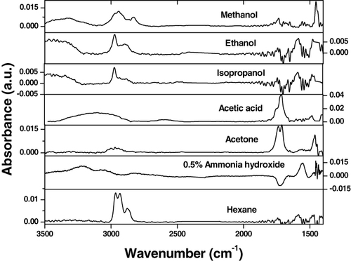
Figure 14. IR spectra of the various analyte vapors obtained with the aid of the two-component (PGMA/PAA) enrichment coating deposited on the Si crystal waveguide.

Nanofoam polymer films as EPLs
The multilayered enrichment coatings developed for optical resonators are examples of the EPL working in a dynamic (‘reversible’) mode. They absorb the vapors of interest during an exposure event. After the exposure, deswelling occurs and the layer returns to its initial state with no post-exposure signature left in the layer. However, for certain applications (e.g. monitoring without power being supplied to a device), it is important to be able to conduct a post-exposure interrogation of the resonators. To this end, we have developed another class of ‘irreversible’ EPL for optical resonators that is capable of retaining the memory of a specific exposure event. This type of EPL is a polymeric nanofoam coating that possesses the behavior of a shape memory material [Citation84, Citation85], exhibiting mechanical action under external stimulus. On exposure to specific analytes, the nanofoam polymeric coatings change their internal structure irreversibly at the nano-level leading to significant changes in the thickness and density. This, in turn, affects the optical properties of the film such as the refractive index and optical absorption.
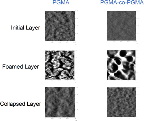
The nanofoam coatings are synthesized by first depositing a film of PGMA or poly(methyl methacrylate-co-glycidyl methacrylate) (PMMA-co-PGMA) random copolymer on the surface of a silicon substrate or micro- resonator via a dip-coating technique [Citation61]. The films are then cross-linked upon the reaction between the PGMA epoxy groups to create a non-soluble but swellable coating. The extent of the cross-linking is controlled to ensure that only a fraction of the epoxy groups is reacted to allow for further functionalization of the film. Finally, the films are swollen in a solvent such as chloroform and freeze-dried under reduced pressure to form a nanofoam anchored to the surface. Prior to foaming, the films can be treated with polymers possessing carboxy groups that have the ability to react with the remaining epoxy group of the PGMA. To prove this concept, we grafted carboxy-terminated polystyrene (PS) to the PGMA and PMMA-co-PGMA films before freeze-drying to obtain the nanofoam coating.
We used ellipsometry and reflectometry to monitor the extent of foaming via thickness measurements. For a 58 ± 3 nm PGMA film, the average foaming was found to be 19 ± 1%. The PMMA-co-PGMA films with a thickness of 42 ± 3 nm foamed on average 23 ± 1%. Figure shows the change in morphology of the coatings upon foaming, and the formation of porous foamed structures can be clearly observed. The nanofoam was found to partially collapse when exposed to various solvents. For example, AFM images of the film exposed to chloroform vapor demonstrate a dramatic change in the nanofoam film morphology after exposure to the solvent (figure ).
Figure 15. Atomic force microscopy (AFM) topographical images of: the initial PGMA layer and PMMA–PGMA layers; the change in the layers’ morphology upon foaming; and the collapsed layers’ morphology upon exposure to chloroform vapor. Image size: 1 × 1 μm, vertical scale: 30 nm.
In our next experiment a 105.5 ± 10 nm film of PS was grafted to PGMA films and 32.7 ± 5.3 nm of PS was grafted to the copolymer film, and the PGMA–PS film was foamed 44 ± 8%. The PMMA-co-PGMA–PS film demonstrated a larger extent of foaming (50 ± 3%). Figure reveals the AFM morphology of the PS functionalized layers before and after foaming. The imaging confirms formation of the porous structure that collapsed upon exposure to solvents.
Figure 16. AFM topographical images of: the initial PGMA–PS layer and PMMA–PGMA–PS layers; the change in the layers’ morphology upon foaming and the collapsed layers’ morphology upon exposure to chloroform vapor. Image size: 1 × 1 μm, vertical scale: 30 nm.

PbTe for mid-IR detection
For photodetection in the mid-IR wavelength regime, semiconductor materials with small, direct band gaps (typically <0.4 eV) are necessary. Common mid-IR photodetector materials include mercury cadmium telluride (HgCdTe) and III–V compounds such as InAs and InSb [Citation86, Citation87]. Lead salts or lead chalcogenides such as PbTe, PbSe and PbS are also used in commercially available detectors for the mid-IRFootnote7. In particular, we have identified PbTe as a promising low-cost mid-IR detector material due to its superior chemical stability, the ease of deposition, and its unique oxygen-sensitization behavior [Citation88, Citation89]. Single crystal and epitaxially grown PbTe have been studied for the fabrication of IR photodetectors and long-wavelength laser devices [Citation90, Citation91]. Our prior work with polycrystalline PbTe thin films has demonstrated high detectivity in the 3–4 μm wavelength range [Citation92]. A further benefit of choosing PbTe is the ability to alloy it with tin telluride (SnTe) to form PbxSn1−xTe. This allows the tuning of the optical band gap to lower values, making it suitable for detection in the 6–12 μm wavelength range.
We have previously conducted systematic studies of the structural, electrical and optical properties of polycrystalline PbTe films obtained from single source thermal evaporation [Citation89, Citation90, Citation92, Citation93]. Our fabrication process yields stoichiometric, polycrystalline films with a rock-salt structure and grain sizes in the order of 50–100 nm. Electrical and optical characterization of the PbTe films shows thermally activated p-type conduction with a mobility of 53 cm2 V−1 s−1, a room temperature carrier concentration of 2.1 × 1017 cm−3 and an optical band gap of 0.386 eV.
Mid-IR chalcogenide glass waveguides monolithically integrated with PbTe detectors
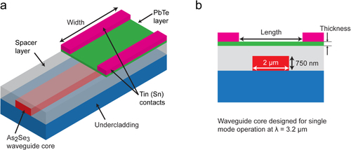
Evanescently coupled detectors using a hybrid integration of III–V detectors (through wafer bonding) for 2.2–2.3 μm detection and monolithically integrated Ge detectors for telecom wavelengths have been demonstrated [Citation94, Citation95]. Hybrid integration schemes can prove to be viable approaches for mid-IR detection, especially when single-crystalline materials are necessary for performance-driven applications. Typically, III–V and II–VI materials for mid-IR photodetectors are grown using techniques such as metal organic chemical vapor deposition or molecular beam epitaxy [Citation86], which have high costs, and monolithic integration is only possible if all the necessary components are grown together. To meet the challenge of on-chip photodetection in the mid-IR, we have developed an integrated sensor design that uses vertical evanescent coupling from ChG waveguides designed for the mid-IR (as shown in section 2.3) into PbTe detectors. The As2Se3 (n = 2.75) core waveguides and the PbTe (n = 5.2) detector layer exhibit a large difference in refractive index that would generally lead to modal mismatch and Fresnel reflections if the PbTe is placed directly over the waveguides. To overcome this limitation, we propose the addition of a low index spacer layer between the waveguide and detector that reduces reflections and enables longer absorption lengths in our PbTe detector. Figure (a) shows the layout of the evanescently coupled detector and figure (b) shows a cross-section of the detector waveguide system. The ChG waveguides are designed for single-mode operation at 3.2 μm and the spacer layer covers the entire sample, with the PbTe extending laterally beyond the waveguide.
Figure 17. (a) Integrated structure with a single-mode (λ = 3.2 μm) As2Se3 waveguide, Ge23Sb7S70 glass undercladding to prevent leakage of the mode into the Si substrate, a low index spacer to minimize modal mismatch and Fresnel reflection, and the photoconductive PbTe layer. (b) The cross-section view of the device. Reproduced with permission from [Citation96].
The photoresponsivity of thermally evaporated polycrystalline PbTe thin films has been analyzed and optimized by comparing films of different thicknesses at room temperature and at thermoelectrically cooled temperatures (− 60 °C or 213 K). Our studies have shown that a 100 nm-thick PbTe detector layer exhibits high photoresponsivity (25 V W−1) in the 3–4 μm wavelength range of interest under a bias current of 0.1 mA at −60 °C [Citation89, Citation92, Citation93]; the responsivity is between 1.2 and 3.5 times larger than a 200 nm-film, pointing to a dependence of responsivity on film thickness. This is an important consideration in our detector design as there is a need to balance the film properties that give the best evanescent coupling with the responsivity of those films.
From three-dimensional finite difference time domain (3D FDTD) simulations carried out at 3.2 μm wavelength, we have determined that the absorption efficiency is maximized with a 90–100 nm-thick PbTe detector layer for a given detector width, a spacer layer index of 1.5 and a thickness of 1.25 μm [Citation96]. This aligns well with our responsivity measurements on PbTe thin films where a peak is achieved at the same thickness values. The length of the detector is limited by the need to maintain a minimum separation between the metal contacts to avoid parasitic absorption losses that can reduce the absorption efficiency in the PbTe layer. The design is flexible enough to be used at near-IR wavelengths and/or with other material systems with appropriate modifications to the device dimensions and choice of spacer layer materials.
To successfully translate the theoretical design summarized above to a practical device, two key requirements have to be satisfied: (a) the identification of a suitable spacer layer material and (b) the formulation of a fabrication path that is compatible with the various materials used in the design.
Spacer layer
The spacer layer material is an important part of our waveguide-integrated detector design. In addition to a relatively low index (1.4–1.6 is ideal), it needs to be transparent to mid-IR wavelengths and easy to deposit on our waveguides. Relatively few materials meet all of these requirements but we have identified some inorganic compounds that are suitable at certain mid-IR wavelength ranges. SiO2 can be used for wavelengths below 3.5 μm where the loss is lower than 0.5 dB cm−1 (for silica glass) [Citation20]. It can be readily deposited using a variety of thin-film deposition techniques such as sputtering and chemical vapor deposition. For wavelengths up to about 5 μm [Citation97], we believe that Al2O3 (deposited via electron beam evaporation or sputtering) is a viable option. Finally, extending the use of our design to still longer wavelengths to take advantage of the wide transparency window of ChGs will likely require alkali halides such as CaF2.
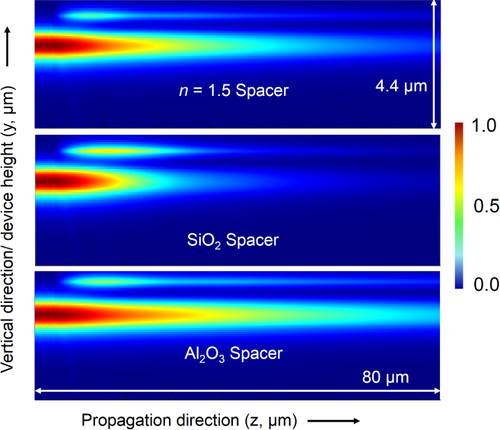
To evaluate the effect of using different spacer layers on our design parameters, we conducted further 3D FDTD simulations. Figure shows how the waveguide-integrated detector design is able to accommodate different materials with different refractive indices (1.43 for SiO2 and 1.65 for Al2O3) by a simple modification of the spacer-layer thickness. The thickness and width of the PbTe layer remain available as further variables that can be optimized to achieve the maximum possible absorption efficiency with any choice of spacer material that fits the criteria described above.
Figure 18. 3D FDTD simulations of the integrated device at λ = 3.2 μm for a 100 nm thick PbTe layer. The side (YZ) cross-section views presented for three different spacer layers exhibit the flexibility of the proposed design: all three materials allow for a gradual absorption of light in the PbTe layer with minimal reflections.
Fabrication of mid-IR integrated PbTe planar detectors
The design we have proposed incorporates disparate materials that need to be integrated together in a monolithic fashion with each successive layer aligned to, and process-compatible with, the previous layer. Starting with mid-IR waveguides and resonators fabricated according to the details presented in section 2.3, we have developed a waveguide-integrated device processing plan that has allowed us to fabricate our first prototype devices designed for 3.2 μm wavelength operation. For this mid-IR wavelength below our 3.5 μm cut-off, we (a) selected SiO2, deposited via plasma-enhanced chemical vapor deposition at a low substrate temperature of 130 °C to avoid heating the ChG layers to their glass transition and to protect them from potentially cracking due to a thermal expansion mismatch with the substrate; (b) developed a suitable photolithography process with NR9-1000PY (negative lift-off resist, Futurrex, Inc.) and a thermal evaporation process for PbTe followed by lift-off in acetone and (c) incorporated a second lithography step to define the electrical contact patterns in resist on an electron beam evaporated tin (Sn) metal contact layer. Resist lift-off is once again performed in acetone accompanied by sonication [Citation33].
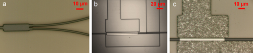
Figure shows optical images taken at different steps along the device fabrication process. The multimode interferometer (MMI) structure shown in figure (a) was designed for a 50–50 split between the two arms with the aim of placing the detector structure on one arm and using the other arm to align the light source to the waveguide. The single-mode (2 μm wide) waveguides gradually taper out to a 5 μm width to improve the alignment tolerance between the PbTe layer and the waveguide. Figure (b) is an optical image of the device before metal deposition, and the final device is shown in figure (c). We observe that the detector and the metal layers are well aligned to each other as well as to the waveguide underneath the spacer layer (not visible as SiO2 is transparent). These prototype integrated detectors are in the process of being experimentally characterized, and their performance will be compared to the results from our FDTD simulations.
Figure 19. (a) MMI waveguide prior to spacer layer deposition; (b) resist pattern for metal contacts aligned to the PbTe layer and (c) final device after metal deposition.
Conclusions
In this work, we have reported on our progress in the area of integrated (on-chip) mid-IR sensing and detection on a silicon platform. We have summarized the material design rationales to achieve low loss, high-quality materials with desired processing compatibility and property tailoring capacity. A pedestal geometry allows us to fabricate mid-IR single crystal silicon waveguides, both with and without an oxide undercladding, for broadband sensing applications based on optical attenuation of the guided light. Fabrication and optical characterization results on chalcogenide glass microdisk resonators and waveguide PhC cavities are reviewed, and preliminary mid-IR spectroscopic chemical sensing results are presented. We have shown that by incorporating EPLs into the sensing system, we are able to distinguish between the responses produced by different organic analytes. We can use this to build sensor systems that produce an optical response only in response to target analytes present in the environment surrounding the sensor. To enable on-chip photodetection in the mid-IR, we have presented a waveguide-integrated photodetector design based on polycrystalline PbTe. By employing a spacer layer material between the chalcogenide waveguide and the PbTe detector, we achieve evanescent coupling to the detector layer. Potential candidates for the spacer layer are discussed, and we have shown fabrication results from our first prototype integrated detectors. We expect that the work presented in this review paper will lead to the further development of compact, highly sensitive and remotely deployable mid-IR optical sensor systems.
Acknowledgments
The authors gratefully acknowledge funding support provided by US Department of Energy (contract number DE-NA000421), NNSA/DNN R&D, the Defense Threat Reduction Agency under award numbers HDTRA1-10-1-0101 and HDTRA1-13-1-0001 and the National Science Foundation under award number 1200406 and EPSCoR grant number EPS-0814251. The authors also would like to thank S Kozacik, M Murakowski and D Prather for assistance with mid-IR device fabrication.
Disclaimer. This paper has been prepared as an account of work partially supported by an agency of the United States Government. Neither the United States Government nor any agency thereof, nor any of their employees, makes any warranty, express or implied, or assumes any legal liability or responsibility for the accuracy, completeness or usefulness of any information, apparatus, product or process disclosed, or represents that its use would not infringe privately owned rights. Reference herein to any specific commercial product, process or service by trade name, trademark, manufacturer or otherwise does not necessarily constitute or imply its endorsement, recommendation or favoring by the United States Government or any agency thereof. The views and opinions of authors expressed herein do not necessarily state or reflect those of the United States Government or any agency thereof.
Notes
7 Lead selenide detectors available from: www.judsontechnologies.com/ lead_sel.html
Related Research Data
References
- HuJSunXAgarwalAKimerlingL 2009 J. Opt. Soc. Am. B 26 1032 10.1364/JOSAB.26.001032
- YuZFanS 2011 Opt. Express 19 10029 10.1364/OE.19.010029
- FarcaGShopovaS IRosenbergerA T 2007 Opt. Express 15 17443 10.1364/OE.15.017443
- HanumegowdaN MSticaC JPatelB CWhiteIFanX 2005 Appl. Phys. Lett. 87 201107 10.1063/1.2132076
- MuneebM 2013 Opt. Express 21 11659 10.1364/OE.21.011659
- ReimerCNedeljkovicMStothardD J MEsnaultM O SReardonCO'FaolainLDunnMMashanovichG ZKraussT F 2012 Opt. Express 20 29361 10.1364/OE.20.029361
- ShankarRLeijssenRBuluILončarM 2011 Opt. Express 19 5579 10.1364/OE.19.005579
- LiuXKuykenBRoelkensGBaetsROsgoodR MGreenW M J 2012 Nature Photon. 6 667 10.1038/nphoton.2012.221
- ChengZChenXWongC YXuKTsangH K 2012 IEEE Photon. J. 4 1510 10.1109/JPHOT.2012.2210700
- ChengZChenXWongC YXuKFungC K YChenY MTsangH K 2012 Opt. Lett. 37 1217 10.1364/OL.37.001217
- SpottALiuYBaehr-JonesTIlicRHochbergM 2010 Appl. Phys. Lett. 97 213501 10.1063/1.3514234
- Baehr-JonesTSpottAIlicRSpottAPenkovBAsherWHochbergM 2010 Opt. Express 18 12127 10.1364/OE.18.012127
- ShankarRBuluILončarM 2013 Appl. Phys. Lett. 102 051108 10.1063/1.4791558
- CharltonCGiovanniniMFaistJMizaikoffB 2006 Anal. Chem. 78 4224 10.1021/ac052214a
- WangXKimS-SRoßbachRJetterMMichlerPMizaikoffB 2012 Analyst 137 2322 10.1039/c1an15787f
- MashanovichG ZMiloševićM MNedeljkovicMOwensNXiongBTeoE JHuY 2011 Opt. Express 19 7112 10.1364/OE.19.007112
- LewiTKatzirA 2012 Opt. Lett. 37 2733 10.1364/OL.37.002733
- TsayCZhaYArnoldC B 2010 Opt. Express 18 26744 10.1364/OE.18.026744
- ZhaYWaldmannMArnoldC B 2013 Opt. Mater. Express 3 1259 10.1364/OME.3.001259
- KitamuraRPilonLJonasM 2007 Appl. Opt. 46 8118 10.1364/AO.46.008118
- Baehr-JonesTPinguetTLo Guo-QiangPDanzigerSPratherDHochbergM 2012 Nature Photon. 6 206 10.1038/nphoton.2012.66
- RoelkensG 2013 Opt. Mater. Express 3 1523 10.1364/OME.3.001523
- YaoYHoffmanA JGmachlC F 2012 Nature Photon. 6 432 10.1038/nphoton.2012.143
- VurgaftmanIBewleyW WCanedyC LKimC SKimMLindleJ RMerrittC DAbellJMeyerJ R 2011 IEEE J. Sel. Top. Quantum Electron. 17 1435 10.1109/JSTQE.2011.2114331
- KhanSChilesJMaJFathpourS 2013 Appl. Phys. Lett. 102 121104 10.1063/1.4798557
- LinP TSinghVKimerlingLAgarwalA M 2013 Appl. Phys. Lett. 102 251121 10.1063/1.4812332
- DuanNLinHLiLHuJBiLLuHWengXXieJDengL 2013 Opt. Mater. Express 3 1537 10.1364/OME.3.001537
- CarlieN 2010 Opt. Express 18 26728 10.1364/OE.18.026728
- YangZLucasP 2009 J. Am. Ceram. Soc. 92 2920 10.1111/j.1551-2916.2009.03323.x
- ShibataSHoriguchiMJingujiKMitachiSKanamoriTManabeT 1981 Electron. Lett. 17 775 10.1049/el:19810544
- ChurbanovM F 1995 J. Non-Cryst. Solids 184 25 10.1016/0022-3093(94)00688-1
- LinP TSinghVHuJRichardsonKMusgravesJ DLuzinovIHensleyJKimerlingL CAgarwalA 2013 Lab Chip 13 2161 10.1039/c3lc50177a
- LinP T 2013 Opt. Mater. Express 3 1474 10.1364/OME.3.001474
- LinP TSinghVCaiYKimerlingL CAgarwalA 2013 Opt. Lett. 38 1031 10.1364/OL.38.001031
- LinP TSinghVLinH-Y GTiwaldTKimerlingL CAgarwalA M 2013 Adv. Opt. Mater. 1 732 10.1002/adom.201300205
- DantoSGiroireBThompsonDWachtelPMusgravesJ DRichardsonK 2013 Int. J. Appl. Glass Sci. 4 31 10.1111/ijag.12008
- CarlieNAnheierN C JQiaoH ABernackiBPhillipsM CPetitLMusgravesJ DRichardsonK 2011 Rev. Sci. Instrum. 82 053103 10.1063/1.3587616
- MusgravesJ DWachtelPNovakSWilkinsonJRichardsonK 2011 J. Appl. Phys. 110 063503 10.1063/1.3638122
- KoontzEBlouinVWachtelPMusgravesJ DRichardsonK 2013 J. Phys. Chem. A 116 12198 10.1021/jp307717q
- KoontzEWachtelPMusgravesJ DRichardsonK 2013 Proc. SPIE 8884 888416 10.1117/12.2029283
- KoontzEZouYOgbuuT OGleasonBWachtelPMusgravesJ DHuJRichardsonK 2013 Proc. SPIE 8884 88841T 10.1117/12.2029274
- MusgravesJ DRichardsonKJainH 2011 Opt. Mater. Express 1 921 10.1364/OME.1.000921
- RichardsonK AMcKinleyJ MLawrenceBJoshiSVilleneuveA 1998 J. Opt. Mater. 10 155 10.1016/S0925-3467(97)00142-0
- EggletonB JLuther-DaviesBRichardsonK 2011 Nature Photon. 5 141 10.1038/nphoton.2011.309
- SongSCarlieNBoudiesJPetitLRichardsonKArnoldC B 2009 J. Non-Cryst. Solids 355 2272 10.1016/j.jnoncrysol.2009.07.015
- NovakSScarpantonioLNovakJPrèM DMartucciAMusgravesJ DMcClenaghanN DRichardsonK 2013 Opt. Mater. Express 3 729 10.1364/OME.3.000729
- NovakJNovakSDussauzeMFarginEAdiametzFMusgravesJ DRichardsonK 2013 Mater. Res. Bull. 48 1250 10.1016/j.materresbull.2012.12.008
- LinHYiZHuJ 2012 Opt. Lett. 37 1304 10.1364/OL.37.001304
- LinH 2013 Opt. Lett. 38 1470 10.1364/OL.38.001470
- LinHLiLDengFNiCDantoSMusgravesJ DRichardsonKHuJ 2013 Opt. Lett. 38 2779 10.1364/OL.38.002779
- HuJTarasovVAgarwalAKimerlingLCarlieNPetitLRichardsonK 2007 Opt. Express 15 2307 10.1364/OE.15.002307
- HuJTarasovVCarlieNPetitLAgarwalARichardsonKKimerlingL 2008 Opt. Mater. 30 1560 10.1016/j.optmat.2007.10.002
- ZouY 2012 Opt. Mater. Express 2 1723 10.1364/OME.2.001723
- NitkowskiAChenLLipsonM 2008 Opt. Express 16 11930 10.1364/OE.16.011930
- RuanYKimM-KLeeY-HLuther-DaviesBRodeA 2007 Appl. Phys. Lett. 90 071102 10.1063/1.2476416
- GaiXLuther-DaviesBWhiteT P 2012 Opt. Express 20 15503 10.1364/OE.20.015503
- HuJCarlieNPetitLAgarwalARichardsonKKimerlingL 2009 J. Light. Technol. 27 5240 10.1109/JLT.2009.2030899
- HuJFengN-NCarlieNPetitLAgarwalARichardsonKKimerlingL 2010 Opt. Express 18 1469 10.1364/OE.18.001469
- HuJ 2010 Opt. Express 18 22174 10.1364/OE.18.022174
- GiammarcoJZdyrkoBPetitLMusgravesJ DHuJAgarwalAKimerlingLRichardsonKLuzinovI 2011 Chem. Commun. 47 9104 10.1039/c1cc12780b
- SolianiA PZdyrkoBLuzinovI 2011 Abstracts of Papers of the American Chemical Society vol 242 186-COLL
- GiammarcoJZdyrkoBHuJAgarwalAKimerlingLCarlieNPetitLRichardsonKLuzinovI 2009 Abstracts of Papers of the American Chemical Society vol 238 170-COLL
- GiammarcoJZdyrkoBPetitLMusgravesJ DHuJAgarwalAKimerlingLRichardsonKLuzinovI 2011 Abstracts of Papers of the American Chemical Society vol 242 194-ANYL
- GiammarcoJZdyrkoBHuJAgarwalAKimerlingLCarlieNPetitLRichardsonKLuzinovI 2010 Abstracts of Papers of the American Chemical Society vol 240 170-COLL
- GiammarcoJHuJAgarwalAKimerlingLCarlieNPetitLRichardsonKLuzinovI 2011 Abstracts of Papers of the American Chemical Society vol 241 201-ANYL
- ZdyrkoB 2009 Abstracts of Papers of the American Chemical Society vol 237 255-COLL
- ZdyrkoBHuJAgarwalAKimerlingLCarlieNPetitLRichardsonKLuzinovI 2008 Abstracts of Papers of the American Chemical Society vol 238 47-ANYL
- SaekiSTsubotaniSKominamiHTsubokawaM 1986 Polym. Sci.: Polym. Phys. Edn 24 325 10.1002/polb.1986.090240209
- JanataJBezeghA 1988 Anal. Chem. 60 R62 10.1021/ac00163a004
- DobbsG TBaluBYoungCKranzCHessD WMizaikoffB 2007 Anal. Chem. 79 9566 9571 9566–71 10.1021/ac070832g
- McLoughlinPFlavinKKirwanPMurphyBMurphyK 2005 Sensors Actuators B 107 170 10.1016/j.snb.2004.11.099
- HeinrichPWyzgolRSchraderBHatzilazaruALubbersD W 1990 Appl. Spectrosc. 44 1641 1646 1641–6 10.1366/0003702904417463
- GobelRKrskaRKellnerRSeitzR WTomelliniS A 1994 Appl. Spectrosc. 48 678 683 678–83 10.1366/000370294774369054
- MurphyBMcLoughlinP 2003 Int. J. Environ. Anal. Chem. 83 653 662 653–62 10.1080/0306731021000015001
- LuzinovaYZdyrkoBLuzinovIMizaikoffB 2012 Analyst 137 333 10.1039/c1an15521k
- LuzinovaYZdyrkoBLuzinovIMizaikoffB 2012 Anal. Chem. 84 1274 1280 1274–80 10.1021/ac201664p
- EastmanM PHughesR CYeltonGRiccoA JPatelS VJenkinsM W 1999 J. Electrochem. Soc. 146 3907 3913 3907–13 10.1149/1.1392571
- PatelS VMlsnaT EFrubergerB 2003 Sensors Actuators B 96 541 563 541–53 10.1016/S0925-4005(03)00637-3
- CareyW PDeGrandpreM DJorgensenB S 1989 Anal. Chem. 61 1674 1678 1674–8 10.1021/ac00190a018
- CarrollG TTurroN JKoersteinJ T 2010 J. Colloid Interface Sci. 351 556 10.1016/j.jcis.2010.07.070
- RaegenAChowdhuryMCalersCSchmatullaASteinerUReiterG 2010 Phys. Rev. Lett. 105 227801 10.1103/PhysRevLett.105.227801
- ZdyrkoBSwaminatha IyerKLuzinovI 2006 Polymer 47 272 10.1016/j.polymer.2005.11.029
- IyerK SLuzinovI 2004 Macromolecules 37 9538 10.1021/ma0493168
- YangBHuangW MLiCLiL 2006 Polymer 47 1348 10.1016/j.polymer.2005.12.051
- LiuCQinHMatherP T 2007 J. Mater. Chem. 17 1543 10.1039/b615954k
- RogalskiA 2003 Prog. Quantum Electron. 27 59 10.1016/S0079-6727(02)00024-1
- RogalskiA 2009 Acta Phys. Pol. A 116 389 (available at http://przyrbwn.icm.edu.pl/APP/ABSTR/116/a116-3-37.html)
- BodeD E 1966 Lead Salt Detectors HaasGThunR E New York Academic
- WangJHuJSunXAgarwalALimDSynowickiRKimerlingL 2008 J. Appl. Phys. 104 053707 10.1063/1.2970163
- WangJZensT WHuJBeclaPKimerlingLAgarwal A M 2012 Appl. Phys. Lett. 100 211106 10.1063/1.4722917
- BöberlMFromherzTRoitherJPillweinGSpringholzGHeissW 2006 Appl. Phys. Lett. 88 041105 10.1063/1.2167396
- WangJHuJBeclaPAgarwalA MKimerlingL 2011 J. Appl. Phys. 110 083719 10.1063/1.3653832
- WangJ 2010 Resonant-cavity-enhanced multispectral infrared photodetectors for monolithic integration on silicon PhD Thesis Massachusetts Institute of Technology, USA (available at http://hdl.handle.net/1721.1/62682)
- GassenqAHattasanNCeruttiLRodriguezJ BTourniéERoelkensG 2012 Opt. Express 20 11665 10.1364/OE.20.011665
- AhnDHongCLiuJGiziewiczWBealsMKimerlingLMichelJ 2007 Opt. Express 15 3916 10.1364/OE.15.003916
- SinghVZensT WHuJWangJMusgravesJ DRichardsonKKimerlingL CAgarwalA 2013 Sensors Actuators B 185 195 10.1016/j.snb.2013.04.065
- PalikE D 1998 Handbook of Optical Constants of Solids London Academic p 761