
Abstract
Organic field-effect transistors (OFETs) are fundamental building blocks for various state-of-the-art electronic devices. Solution-processed organic crystals are appreciable materials for these applications because they facilitate large-scale, low-cost fabrication of devices with high performance. Patterning organic crystal transistors into well-defined geometric features is necessary to develop these crystals into practical semiconductors. This review provides an update on recentdevelopment in patterning technology for solution-processed organic crystals and their applications in field-effect transistors. Typical demonstrations are discussed and examined. In particular, our latest research progress on the spin-coating technique from mixture solutions is presented as a promising method to efficiently produce large organic semiconducting crystals on various substrates for high-performance OFETs. This solution-based process also has other excellent advantages, such as phase separation for self-assembled interfaces via one-step spin-coating, self-flattening of rough interfaces, and in situ purification that eliminates the impurity influences. Furthermore, recommendations for future perspectives are presented, and key issues for further development are discussed.
Introduction
For more than three decades, efforts exerted by the academic and industrial sectors have focused on the applications of organic semiconductors in electronics [Citation1–Citation4]. It is of great interest to examine the history and development of organic electronics. This research field initially started from a unique laboratory observation of electronic conductivity from a polymer that was believed to be insulating. Over the past decades, we have experienced many interesting breakthroughs on fundamental and inherent limitations, especially for electrical properties, such as carrier mobility [Citation5–Citation10]. Many state-of-the-art electronic products based on organic materials possess several advantages over their inorganic counterparts. Organic field-effect transistors (OFETs) are fundamental building blocks in circuits; OFETs primarily act as switches and/or signal-processing elements for applications ranging from active matrix displays to radio-frequency identification tags [Citation11–Citation14]. The first OFETs were fabricated in the early 1980s using polymers or small-molecule semiconductors [Citation15–Citation19]. However, OFETs have poor device performance; particularly, the low field-effect mobility (μ FET) of OFETs limits the applications of devices [Citation20–Citation22]. This poor performance is mainly attributed to the active conduction channels exhibiting as amorphous or polycrystalline thin films. In addition, the device characteristics based on these thin films are strongly affected by the imperfections of the film structure and by the insufficient purity of the organic materials.
Continuous improvement in device performance is a key factor that determines the development of OFETs. Other factors, such as the steady decrease in fabrication cost and applicability, are also deemed critical. Recent studies have considered solution-processed organic semiconducting crystals as ideal candidates for high-performance and low-cost OFETs [Citation23–Citation46]. Organic crystals often yield better device performance than their counterparts in amorphous or polycrystalline thin films because of the perfectly ordered molecules that improve intermolecular interaction via close molecular packing [Citation47]. Grain boundaries and molecular disorder, which limit charge transport by scattering the charge carriers, can be greatly reduced in crystals [Citation48]. Since the first successful fabrication of organic crystal FETs ten years ago, the charge carrier mobility extracted from organic crystal FETs has reached 20–40 cm2 V−1 s−1 [Citation49–Citation58]. The semiconducting crystals used in the active channel are insoluble small molecules, whereas solution-based techniques are counted out of the fabrication schemes for organic crystal FETs. Solution-based processes can significantly reduce the device fabrication cost because sophisticated and expensive facilities, such as those for photolithography or high-temperature and/or high-vacuum processing, are not required. With the development of technologies for the design and synthesis of organic materials, solution-processed, small-molecule semiconductors that can form into crystalline phases involving strong intermolecular interaction have been extensively reported in the literature. Thereafter, a new challenge for further development of OFETs emerged. Applications of OFETs can be broadened upon improvement of electrical performance and upon fabrication of devices on different substrates, such as flexible and paper-based types.
Although organic crystals are considered promising materials for high-performance and low-cost electronic devices, fabrication of solution-processed organic crystal FETs still poses a challenge in patterning technology [Citation40, Citation59–Citation63]. Insoluble organic semiconductors can be deposited by thermal evaporation in a vacuum and generate thin-film patches according to the patterns of shadow masks; by contrast, solution-processed materials lack patterning capability and normally cover the entire substrate surface with uniform thin films. In particular, as in the case of organic crystals, organic molecules can self-assemble into crystalline phases with highly ordered molecular packing, whereas crystals exhibit random distributions with peculiar deposition positions on the substrate surface. This is because the intermolecular force (van der Waals force) in organic crystals is weak in nature and easily influenced by experimental conditions, such as temperature and solvent evaporation, during crystallization [Citation64, Citation65]. The development of patterning techniques for organic crystals deposited on well-defined geometric features is crucial to stimulate the application of organic crystals in electronics. These techniques have advantages for mass production and for reduction in the leakage current and crosstalk between neighboring devices, especially when common gate electrodes are applied.
In this review, we focus on the patterning technology for solution-processed organic crystals and their applications in OFETs. Numerous recent studies have reported that OFETs based on solution-processed, small-molecule crystals exhibit excellent performance [Citation36]. Topical reviews on polymer semiconducting crystals are also recommended for readers [Citation46]. In section 2, we discuss the patterning techniques associated with spin-coating. The basic strategy in applying surface wettability modification is explored in detail, and our recent development of patterned organic crystals using spin-coating solutions is reviewed. Other solution-assisted processes for patterning organic crystal transistors, such as inkjet printing, micropatterning with nucleation control, and solution shearing, are examined in section 3. Table summarizes the features of typical patterning techniques for solution-processed organic crystals, which are mainly discussed in sections 2 and 3. In section 4, we describe the organic crystal growth and device physics of organic crystal FETs. We also share our opinions on the future development of these transistors.
Spin-coating processes for patterned organic crystals and their applications in OFETs
Patterning techniques for solution-processed organic crystals
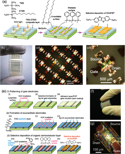
Various approaches for the patterning of solution-processed organic crystals have been proposed. The utilization of self-assembled monolayers (SAMs) is the first successful attempt for patterning vapor-grown organic crystals by controlling nucleation location [Citation26, Citation60, Citation62, Citation66, Citation67]. This approach is commonly used for solution-processed organic crystalline semiconductors. Patterning involves the surface modification of substrate into wettable and dewettable regions with different functional groups of SAMs [Citation26, Citation40, Citation68–Citation71]. Minari et al [Citation69, Citation72] developed a surface selective deposition method to fabricate OFETs with organic crystalline films as semiconducting channels (figures (a)–(d)). Surface regions modified by alkyl or fluoroalkyl groups exhibit dewettable or solution-repellent property, whereas those functioned by phenyl groups have more favorable surfaces for the deposition of organic semiconductors. When an organic semiconductor is deposited from the solution using spin-coating, small droplets are only confined in the patterned region wettable to the solution, forming polycrystalline organic films as active channels. This method is extended for the all-solution fabrication of OFETs on transparent flexible substrates (figures (e)–(g)) [Citation71]. SAMs can also be applied for insoluble organic materials, such as rubrene, pentacene, and fullerene C60, which are deposited via physical vapor transport in vacuum to form patterned crystals [Citation60, Citation62]. Crystal nucleation is effectively suppressed in smooth regions, whereas the rough SAM domains act as effective primary nucleation centers. Hence, this principle is different from that for solution-processed materials.
Figure 1 (a) Schematic of the fabrication of self-organized organic crystal FET arrays on a flexible substrate; TMS = tetramethoxysilane, DTMS = decyltrimethoxysilane. (b) Photograph of organic crystal FETs on a flexible transparent substrate. (c) Cross-polarized microscopy image of the OFET arrays. (d) Optical microscopy image of an individual transistor showing the channel region comprising the organic crystals. (e) Fabrication of all-solution-processed organic crystal FETs on a flexible substrate; VUV = vacuum ultraviolet, FAS = fluoroalkylsilane, PVP = polyvinylphenol. (f) Photograph of the OFET arrays. (g) Cross-polarized microscopy image of the channel region of an OFET. (Reproduced with permission from [Citation69, Citation71] © 2009 AIP Publishing and © 2010 The Japan Society of Applied Physics.)
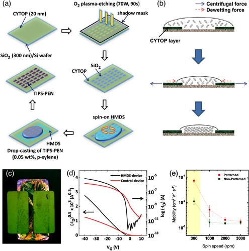
Surface modification by SAMs to introduce different wettability regions prior to the deposition of organic materials is the most common method for patterning organic semiconductors. SAM growth typically takes several hours. The hydrophobic and solution-processed fluoropolymer CYTOP can be used as the raw material for patterning techniques to shorten the processing time for device fabrication. CYTOP is highly hydrophobic with a water contact angle of ∼110°. In addition, this fluoropolymer cannot be detached from the substrate by organic solvents, such as chloroform, acetone, and toluene. Surface patterning can be designed using simple shadow-mask plasma etching because the C–F bonds in the CYTOP are broken by O2-plasma. The covered area remains hydrophobic, whereas the exposed region becomes hydrophilic and well wettable for the solution. Kim et al [Citation73] studied OFETs using the organic semiconductor 6, 13-bis(triisopropylsilylethynyl) pentacene (TIPS-PEN, figures (a)–(d)). The wettability of the SiO2 surface is controlled by patterning an amorphous CYTOP thin film using O2-plasma etching. TIPS-PEN solution is then drop-cast and selectively crystallized on the plasma-etched area. Patterning processes, including ablation or removal of hydrophobic polymer layers, often suffer from the degradation of device performance because of the contamination on the dielectric surface and the increased number of trap states at the semiconductor/insulator interfaces. Modification of the patterned SiO2 area with hexamethyldisilazane is efficient in reducing the number of interfacial traps. Thus, high-performance devices can be obtained from patterned TIPS-PEN OFETs with a μ FET of 0.19 cm2 V−1 s−1, a subthreshold swing (SS) of 0.74 V/decade, and an on/off ratio of 107. Further analysis shows that the crystalline part of TIP-PEN in the patterned region is influenced by solvent evaporation and that the adoption of a patterned CYTOP thin film induces crystal growth in three dimensions (figure (e)) [Citation74].
Figure 2 (a) Fabrication of patterned TIPS-PEN crystal FETs. Surface patterning was carried out using spin-coating of CYTOP and subsequent exposure to shadow-mask O2-plasma etching; HMDS = hexamethyldisilazane. (b) Illustration of the mechanism for the formation of TIP-PEN films on a patterned substrate. (c) Cross-polarized microscopy image of a single OFET with TIPS-PEN well confined in the patterned region. (d) Typical transfer characteristics of the TIPS-PEN OFET. (e) Variation of the carrier mobility with spinning speed on nonpatterned and patterned substrates. (Reproduced with permission from [Citation73, Citation74] © 2008 AIP Publishing and © 2012 American Chemical Society.)
These patterning techniques are based on the modification of surface wettability prior to the deposition of organic semiconductors from solutions. Some solution deposition facilities, such as inkjet printing, have intrinsic capabilities in patterning functioning materials to desired positions (section 3).
Spin-coating from mixture solutions for patterned organic crystals
Previous studies demonstrated various approaches contributing to the patterning of solution-processed organic semiconductors. High electrical performance is frequently achieved from related OFETs when organic materials with strong intermolecular forces are used. Spin-coating from a semiconductor/insulator mixture solution exhibits distinct advantages that are beneficial for the application of OFETs [Citation75, Citation76]. The main principle lies in the self-assembly of semiconductor/insulator interfaces during spin-coating. A double-layer structure with separated materials can be obtained directly via spin-coating from the mixture solution. Vertical phase separation is driven by solute–substrate, solute–solvent, and solute–solute interactions.
When combined with patterning techniques, unique research results have been obtained. In this section, we mainly demonstrate our recent progress in this research field. In section 2.2.1, we demonstrate the fabrication of transistor arrays based on patterned rod-like single crystals grown via solvent vapor annealing (SVA). Further improvement in device uniformity is directly achieved from large, plate-like crystals via a simple spin-coating process (section 2.2.2). In section 2.2.3, we further apply our technique to pattern organic crystal transistors on various substrates, including those based on plastic and paper. Finally, we present an inherent in situ purification of our method that can eliminate the influence of impurities, allowing the direct usage of low-purity materials for device fabrication.
Growth of patterned, rod-like single crystals using solvent vapor annealing
Surface selective deposition using SAMs is an efficient approach to pattern-functioning materials on a substrate surface. Previous works have applied this technique to plastic substrates and all-solution-processed devices, where polycrystalline organic semiconductors serve as channel materials. The grain boundaries among crystals can affect the charge transport via charge trapping and scattering; hence, patterned single crystals are of great interest for the achievement of high-performance device arrays.
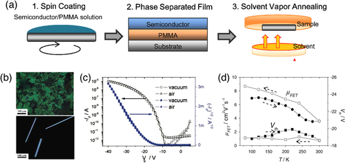
Tremendous efforts have been exerted to develop solution-assisted and low-cost processes to fabricate organic semiconducting single crystals. High-quality organic single crystals can exhibit larger mobility than amorphous silicon devices. Solvent vapor exposure induces grain growth and amorphous-to-crystalline or polymorphic transformations in molecular organic thin films [Citation77–Citation81]. Thus, we applied the simple post-treatment of SVA for the growth of organic single crystals recrystallized from a polycrystalline semiconductor/polymer insulator bi-layer structure that was self-assembled during a spin-coating process from a solution (figure (a)) [Citation61, Citation75, Citation82]. Vertical phase separation via spin-coating is attributed to surface energy differences for each component [Citation83–Citation87]. Crystals demonstrate high performance when the mobility based on the transistor structure is ∼10 cm2 V−1 s−1.
Figure 3 (a) Illustration of polymer-assisted solvent vapor annealing (PASVA). 1. Spin-coating the mixture solution of semiconductor and PMMA; 2. spontaneous vertical phase separation, leading to the formation of bilayer structure; 3. placement of the sample in a Petri dish half-filled with solvent for solvent vapor annealing (SVA) under ambient conditions at room temperature. (b) SVA can stimulate the rearrangement of organic semiconductor, and it changes from a polycrystalline thin film (top) to isolated rod-like crystals (bottom). (c) Transfer curves measured under vacuum and in air, showing high device performance and good stability under ambient conditions. (d) Temperature dependence of the field-effect mobility (μ FET) and threshold voltage (V th), indicating a band-like charge transport behavior obtained in the organic crystals fabricated via SVA. (Reproduced with permission from [Citation43] © 2011 WILEY-VCH Verlag GmbH & Co. KGaA, Weinheim.)
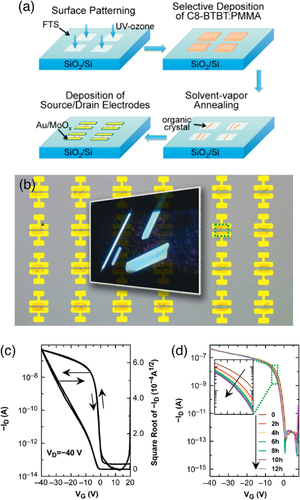
Surface selective deposition methods for SAMs and SVA were combined to fabricate patterned organic crystal OFET arrays [Citation68]. A solution of dioctylbenzothienobenzothiophene (C8-BTBT) and polymethylmethacrylate (PMMA) was spin-coated onto the SiO2 surface with patterned wettability (figure (a)). The sample was treated through SVA for the recrystallization process. As shown in figure (b), only rod-like C8-BTBT single crystals were formed via SVA-stimulated self-assembly in the patterned region. MoO3 and Au were evaporated to form the source and drain electrodes, leading to the fabrication of crystal-based OFETs into the bottom-gate top-contact structure. The devices exhibited high performance with a μ FET of 3.5 cm2 V−1 s−1 and an on/off ratio of more than 107 (figure (c)). Bias-stress measurement was carried out, and a good electrical reliability of the devices with μ FET maintained within a small range of magnitude was observed (figure (d)). This observation indicates that charge trapping in pre-existing or stress-generated deeply localized states in the crystal bulk and at the dielectric interfaces is limited despite the fabrication under ambient conditions with oxygen and water. However, the organic crystal transistor arrays showed large variation in μ FET because of differences in contact resistance due to variations in crystal thicknesses. Further analyses on the influence of device architectures confirm that the contact resistance can affect transistor performance and that the top-gate top-contact structure exhibits high mobility (7.4 cm2 V−1 s−1) and small device-to-device variation [Citation70].
Figure 4 (a) Fabrication of patterned organic single crystal transistors. (b) Microscopy image of patterned C8-BTBT crystal transistor arrays. The middle portion shows the cross-polarized microscopy image of crystals in the channel as highlighted by a green dotted square. (c) Transfer characteristics and (d) bias-stress measurement of a C8-BTBT crystal transistor. (Reproduced with permission from [Citation68] © 2011 Authors).
Large plate-like organic crystals with high uniformity
Significant development has been achieved for patterned organic crystal transistors with continuous improvement in device performance and large numbers of crystal growth methods. However, some industrial standards limit the future applications of organic semiconducting materials. Among these obstacles, uniformity in electrical performance with reduced variation from device to device and from batch to batch is often seriously considered when organic crystals are used as channel materials in FETs [Citation63, Citation69, Citation88]. Variation in the performance of organic crystal transistors can be attributed to the orientation and alignment of crystals, causing anisotropy of charge transport and variances in the width and length of active channels [Citation37, Citation89, Citation90]. Morphological characteristics are also important; contact resistance can be affected by crystal thickness [Citation68, Citation72]. Large, plate-like organic crystals with small thicknesses are potential candidates for FET arrays with minimal performance fluctuations because these crystals can provide morphologically uniform films.
However, the formation of organic crystals into thin, plate-like, and large-size shapes is difficult to achieve because the orientation of organic crystal growth generally follows the crystal axes [Citation27, Citation43, Citation67, Citation91–Citation96]. Therefore, post-treatment after deposition that allows rearrangement of organic molecules is necessary. For instance, Lee et al [Citation97] reported an abrupt thermal annealing method for rubrene thin films deposited onto SiO2 substrate using thermal evaporation. The heating process was carried out by placing as-deposited rubrene films on a preheated hot plate set at 170 °C in a nitrogen environment for one minute. Continuous crystalline films consisting of large-sized and plate-shaped domains were created over the entire substrate surface, which is distinct from a typical rubrene crystal with a hexagonal shape.
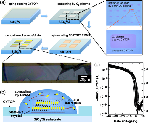
Our work demonstrated the growth of large, plate-like organic crystals by the combination of a patterning technique using a hydrophobic polymer and a spin-coating process from a semiconductor/insulator solution (figure (a)) [Citation23]. The hydrophobic polymer CYTOP was spin-coated onto the SiO2 substrate; the surface of the substrate was then patterned using O2-plasma by a shadow-mask, reactive-ion etching system. This process is similar to methods using SAMs, wherein the surface wettability is patterned into hydrophobic and hydrophilic regions with portions unexposed and exposed to plasma. A spin-coating process from an anisole solution of C8-BTBT and PMMA produces large plate-like C8-BTBT crystals confined in the patterned regions, and a phase separation leads to a thin PMMA layer underneath the crystals [Citation43, Citation76]. Figure (b) shows that the strong molecular interaction and large-distance movement of C8-BTBT molecules stimulate the formation of organic crystals, assisting PMMA in spreading on the surface of patterned regions. CYTOP-patterned regions have a vertical structure with a depth of ∼40 nm, whereas patterned SAMs exhibit a 2D modification strategy. The CYTOP sidewall, which enhances the spreading of PMMA, is essential in the formation of large, plate-like C8-BTBT crystals via spin-coating. High uniformity was obtained simultaneously for the carrier mobility, threshold voltage, and subthreshold swing when the device performance of OFETs based on these crystals was measured (figure (c)). Good uniformity in device performance for organic crystals is critical for applications in active-matrix displays. Material concentrations can influence the electrical performance of the devices; the highest mobility we obtained was up to 1.5 cm2 V−1 s−1.
Figure 5 (a) Fabrication of field-effect transistor arrays based on patterned plate-like organic crystals using hydrophobic dielectric of CYTOP. The organic crystals are formed using a simple spin-coating process from a blend of C8-BTBT and PMMA. (b) Illustrative representation of the solution on the surface of the patterned region, showing that the formation of plate-like organic crystals can be attributed to the strong molecular interaction and large-distance movement of C8-BTBT molecules, with the assistance of the PMMA spreading on the highly hydrophilic surface of the patterned regions. (c) Transfer curves of the transistor arrays based on the C8-BTBT crystals. (Reproduced with permission from [Citation23] © 2011 Elsevier.)
Organic crystal FETs on various substrates, including plastic and paper
Aside from the continuous improvement in the device performance of OFETs, extension of their applications is another primary factor for the future development of organic electronics. For instance, devices on flexible substrates are highly attractive for various state-of-the-art electronics [Citation98–Citation103]. Although solution-processed semiconducting organic crystals are ideal materials for high-performance and low-cost devices, most processes involved in organic crystals grown on flexible substrates do not have a patterning capability. Demonstrating the application of organic semiconducting crystals deposited from a solution in flexible OFETs, we applied our technique to fabricate patterned organic crystals on flexible PEN substrates [Citation104]. As shown in figure (a), device arrays were fabricated on a PEN substrate with the bottom-gate top-contact structure. A 540 nm-thick CYTOP layer was spin-coated onto the substrate with evaporation-deposited Au bottom-gate electrode arrays and then patterned through a shadow-mask O2-plasma. The CYTOP layer in the patterned region also acted as the gate insulator with a thickness of ∼500 nm. A solution of C8-BTBT and PMMA was spin-coated onto the substrate and merely confined within the patterned regions. The device fabrication was completed by subsequent deposition of MoO3 and Au to form the source and drain electrodes. C8-BTBT crystals were observed in the patterned regions with grain sizes as large as hundreds of micrometers (figures (b)–(d)). The as-fabricated devices can exhibit a typical transistor behavior with a μ FET of 0.22 cm2 V−1 s−1, an SS of 0.7 V dec−1, a V T of 1.3 V, and an on/off ratio of 107.
Figure 6 (a) Fabrication of flexible FET arrays based on patterned solution-processed C8-BTBT crystals. (b) Photograph and (c) microscopy image of a flexible PEN substrate with solution-processed organic crystal FET arrays. (d) Cross-polarized microscopy image of the patterned C8-BTBT crystals in the channel region. (e) FET arrays fabricated on paper substrate with solution-processed organic crystals confined in patterned regions. (f) Structure of FETs with C8-BTBT crystals, and diagram of the roughness at different surfaces from the bare paper substrate to the PMMA layer. (g) Cross-polarized microscopy image of the C8-BTBT crystals in the patterned region. (h) AFM topographic image of a patterned region after rinsing in cyclohexane. The PMMA surface is exposed and partially covered with C8-BTBT. (i) The AFM profile taken across the broken line over a patch in (h), consistent with the length of the C8-BTBT molecule. (Reproduced with permission from [Citation24, Citation104] © 2012 Elsevier and © 2013 Authors.)
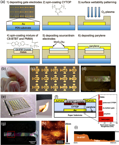
Paper is the cheapest substrate at present. The price of paper substrates is lower (∼0.1 cent dm−2) than that of plastic substrates (polyethylene naphthalate: ∼2 cent dm−2; polyimide: ∼30 cent dm−2). Paper is also highly compatible for rapid manufacturing processes, such as spray-coating and roll-to-roll printing. Considerable progress in paper electronics has demonstrated the fabrication of functioning devices with organic semiconductors on paper substrates [Citation105–Citation116]. The resulting devices possess distinct application perspectives that are not achieved by rigid and flexible plastic substrates. The fabrication of high-performance FETs is still an immense challenge. The principal obstacles include the large surface roughness of paper substrates and the difficulty in specific surface modification for patterning using SAMs. Although organic crystals with highly ordered molecules are promising for the achievement of high-performance devices, large paper surface roughness can increase the number of nucleation sites during the crystallization of organic materials. We present our proposed method to fabricate high-performance OFETs based on patterned organic semiconducting crystals to eliminate issues with paper surface roughness [Citation24]. We used a commercially available photo paper as the substrate. A protective layer of parylene that can resist water and chemicals was coated because of the high water absorption property of paper. As shown in figures (e) and (g), the devices on paper were fabricated similar to those on PEN substrate, except that the source and drain electrodes were formed by successive evaporation of FeCl3 and Au. The insertion layer of FeCl3 between the Au and organic semiconductor can introduce a highly chemically doped contact that significantly reduces the contact resistance [Citation117]. Although bare paper had large surface roughness (rms roughness of ∼48 nm) and parylene film coating reduced the roughness to ∼16 nm (figure (f)), the resulting organic crystal FETs yielded outstanding device performance, exhibiting high μ FET (1.3 cm2 V−1 s−1), large on/off ratio (>108), and low SS (2.0 V dec−1). To the best of our knowledge, our proposed method is the first to hold the capability in simultaneously patterning the paper substrates and the growth of organic crystals on paper. Our devices with solution-processed organic crystals on paper still possess the highest device performance in terms of both carrier mobility and on/off ratio for OFETs on paper, even when compared with devices based on vapor-deposited organic semiconductors. The excellent performance on paper is attributed to the reduction in interfacial roughness because spin-coating from the mixture solution naturally creates a smooth C8-BTBT/PMMA interface brought by vertical phase separation [Citation43, Citation44, Citation75, Citation76, Citation118]. After the sample was rinsed in cyclohexane to expose the underlying PMMA surface by removing the C8-BTBT upper layer, the atomic force microscopy (AFM) results showed a very smooth surface (rms roughness: ∼3 nm) of the PMMA layer despite being partially covered with some remaining C8-BTBT (figures (h) and (i)). Some C8-BTBT patches with sizes of hundreds of nanometers and molecular smoothness were also observed. The thicknesses of these patches were consistent with the length of the C8-BTBT molecule, indicating the high-quality morphology of the C8-BTBT/PMMA interface. The results suggest that our OFET fabrication method has no critical requirement for the surface smoothness of the substrate.
In situ purification of organic semiconductors
The history of the semiconductor manufacturing industry shows that the steady decline in production costs can account not only for the industry’s continuous improvement in performance/reliability and extension of applications but also for the industry’s fast growth [Citation119]. The aim to decrease manufacturing costs is also a determinant factor for the rapid development of solution-processed organic electronics, which offer low-temperature and large-area device processing. Organic channel materials for device fabrication must have high purity because impurities (e.g., the by-products of material synthesis) can induce traps that capture charge carriers, thereby degrading the transport of charge in a device [Citation8, Citation88, Citation98, Citation120–Citation123]. The semiconductor industry uses electronic-grade solvents and chemicals because the impurities in these chemicals are one of the factors that reduce the yield per wafer, consequently increasing the cost per saleable unit. Electronic grade would have lower purity than the one currently manufactured should this industry be able to achieve the same performance with low-purity, raw materials. In the traditional semiconductor industry, most expenses originate from infrastructure, equipment, and processing rather than from the chemicals used. Thus, the cost of ultra-pure raw materials can be neglected. By contrast, the organic semiconductor and fabrication process comprise the bulk of the total cost, with low-cost strategies involved in organic semiconductors. Purification of organic materials can increase production costs and can be time consuming, and loss of active materials during purification can be significant. Therefore, we demonstrated a solution-processed fabrication technique that can directly use as-synthesized, low-purity materials for the application of organic crystal transistors.
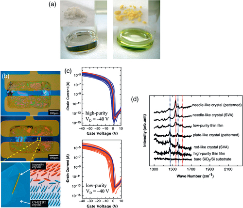
Our patterning technique assisting the spin-coating process from solutions can provide an in situ purification that inherently removes impurities from the active materials [Citation124]. As shown in figure (a), high-purity (>98%) C8-BTBT is in the form of white powder, whereas the as-synthesized low-purity (∼92%) C8-BTBT is in the form of yellow powder. The impurities have a significant effect on the performance of OFETs based on the polycrystalline uniform films spin-coated from the bare C8-BTBT solution, resulting in remarkable degradation in electrical performance as compared with the devices based on the high-purity material. C8-BTBT was blended with PMMA in solution and then spin-coated onto the patterned CYTOP surface. The fabricated transistor arrays based on C8-BTBT crystals with different purities exhibited nearly identical performance in all transistor parameters, including μ FET, SS, V T, and on/off ratio (figure (c)). Further analyses using cross-polarized optical microscopy and micro-Raman spectroscopy revealed that the impurities were excluded to recrystallize into needle-like crystals during the spin-coating process. These impurities floated on top of the active plate-like crystals with large grain size (figures (b) and (d)). The in situ purification that eliminates the influence of impurities depends on three key factors. One is the vertical phase separation forming the PMMA-bottom, C8-BTBT-top structure. This structure naturally takes place during the spin-coating process and is attributed to the differences in the surface energy of each component [Citation85–Citation87]. The other is the recrystallization of C8-BTBT and the impurity during the spin-coating process. C8-BTBT starts crystal nucleation and growth before the impurity during solvent evaporation because C8-BTBT has higher concentration in the solution than the impurity. Finally, the PMMA spreading effect facilitates the formation of large C8-BTBT crystals covering the patterned regions thoroughly. The impurity crystals are separated vertically and are floating on top of the large C8-BTBT crystals, making no contribution to the conduction in the channel. To the best of our knowledge, our work is the first to demonstrate a processing technique that can directly use low-purity materials for the fabrication of high-performance devices. With the proposed technique, devices based on low-purity materials have performance comparable with those of devices based on high-purity materials.
Figure 7 (a) Optical images of the C8-BTBT solutions prepared with high- (left) and low-purity (right) C8-BTBT. (b) Cross-polarized microscopy images of typical C8-BTBT plate-like crystals in patterned regions from high- (upper) and low-purity (middle) PMMA-blended C8-BTBT solutions. (Lower left) cross-polarized microscopy image of the small needle-like crystal in the yellow-dotted square in (middle). (Lower right) illustration of the in situ purification during spin-coating with impurity (red ellipsoids) and C8-BTBT (blue ellipsoids) molecules. (c) Transfer curves of the FET arrays based on patterned C8-BTBT crystals from high- (upper) and low-purity (lower) materials. (d) Micro-Raman spectroscopy characterizations in the region for thiophene peaks for the thin films, the patterned crystals from direct spin-coating, and the crystals from solvent vapor annealing (SVA). We observe that the needle-like crystals from both spin-coating and SVA are formed by impurity molecules, whereas the plate-like and rod-like crystals are formed by C8-BTBT molecules. Spectral data from a bare SiO2/Si substrate are shown for comparison, indicating that the peaks do not originate from the SiO2/Si substrate. (Reproduced with permission from [Citation124] © 2013 The Royal Society of Chemistry.)
Other solution-assisted processes for patterning organic crystal transistors
The patterning technologies discussed in section 2 are primarily based on the modification of surface wettability prior to the spin-coating process. Many emerging methods, such as inkjet printing and micro-patterning with nucleation control regions, can directly produce patterned organic crystals via other solution-based techniques. Some approaches that can efficiently stimulate organic crystal growth in solution involve patterning technology to enhance the quality of grown crystals. Some typical and important techniques are thus described and examined.
Inkjet printing
Printing technology typically releases the ink out of the nozzles to deposit onto a substrate surface such as paper, allowing the reproduction of print materials. When the ink changes into a solution with a dissolved or dispersed organic semiconductor or conductor, the printing turns out to be useful for organic electronic devices at a micrometer resolution. Robust and versatile techniques extensively used in the microelectronics industry can be avoided because of the solution-based processing and intrinsic patterning capability of inkjet printing. This method can significantly reduce manufacturing costs. Inkjet printing initially emerged as an attractive depositing and patterning technique for conjugated polymers in light-emitting diodes and full-color, high-resolution displays. Inkjet printing is beneficial to OFETs based on disordered polymers because nearly all small-molecule semiconductors are still insoluble at that time [Citation5, Citation125].
When using small-molecule semiconducting materials (TIP-PENS and C8-BTBT) with strong intermolecular forces, crystalline droplets or thin films with controlled morphologies as conducting channels can also be deposited using inkjet printing [Citation126–Citation130]. Lim et al [Citation131] used TIP-PEN as the organic semiconductor dissolved in chlorobenzene as the major solvent mixed with 25% of the minor solvent. The released drop falls under the action of gravity and air resistance until it impinges on the substrate and spreads under momentum acquired in the motion. Surface tension aids the surface flow, and the drop dries out through solvent evaporation. They used a solvent mixture to balance the Marangoni and convective flows in the drying droplet, consequently controlling the morphology of the dried droplet. Other methods also show good control of the nucleation and crystallization of inkjet-printed organic semiconductors. These methods include inducing external electrical field [Citation132], applying bank structure to confine the droplets [Citation126], and changing the substrate temperature [Citation129].
Furthermore, experiments show that applying the blend solution of a small-molecule semiconductor and polymer insulator can improve the device performance of inkjet-printed OFETs [Citation133]. A blend of TIPS-PEN and polystyrene (PS) was deposited using an inkjet process to form OFETs with a bottom-gate bottom-contact structure. Pure TIPS-PEN deposited onto the substrate exhibited a crystalline phase with irregular shapes, covering only partially on transistor channels. Meanwhile, the addition of PS led to spherical TIPS-PEN deposits with large domain size and improved crystal morphology that covered the entire device area. The OFETs fabricated from the blend solution possessed high transistor performance, exhibiting a maximum mobility of 1.5 cm2 V−1 s−1 and an on/off ratio of more than 107. Polymers can also enlarge crystal size and improve device behavior when inkjet prints small-molecule semiconductors onto the polymer substrate [Citation134].
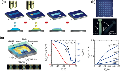
A recent breakthrough has revealed that inkjet-printed organic single crystals yield OFETs with carrier mobility as high as 31.3 cm2 V−1 s−1 [Citation36]. A novel double-shot inkjet printing technique assisted by patterning of substrate surface wettability was proposed. As illustrated in figure (a), an antisolvent crystallization ink (N,N-dimethylformamide) with very low solubility for the organic semiconductor of C8-BTBT was first deposited from an ink-jetting nozzle, and then C8-BTBT in dichlorobenzene solution was overprinted on the deposited crystallization ink. The formed intermingled droplet was confined in the solvent-wetting patterned region, and a slow crystalline film growth of C8-BTBT was observed at the droplet surface. The resulting semiconductor thin films covering the patterned regions exhibited a single-domain characteristic. As shown in figure (b), the OFETs based on C8-BTBT single crystals yielded very high mobility in the saturation region, reaching average and maximum values of 16.4 cm2 V−1 s−1 and 31.3 cm2 V−1 s−1, respectively. The devices showed typical output behavior. The value of mobility nearly reached the fundamental limit at room temperature, considering that the fabrication process was performed under ambient conditions. The devices based on inkjet-printed organic single crystals also exhibited good performance in terms of on/off current ratio (105 to 107) and SS (∼2 V dec−1), with a threshold voltage of ∼10 V. The device characteristics were not degraded by more than 10% after the films were kept in air for eight months. However, a large variation in carrier mobility and critical contact effect was observed in output curves, leaving a lot of room for technique improvement.
Figure 8 (a) Schematic of inkjet printing of organic single-crystal thin films. Antisolvent ink (A) is first inkjet-printed (step 1), and the solution ink (B) is overprinted sequentially to form intermixed droplets confined to a predefined area (step 2). Semiconducting thin films grow at liquid–air interfaces of the droplet (step 3) before the solvent fully evaporates (step 4). (b) (Upper) cross-polarized microscopy image of an array of inkjet-printed C8-BTBT single-crystal thin films. (Lower) cross-polarized micrographs of the film. (c) (Left) illustration of the device structure and micrograph of the thin-film transistors. (Right) transfer and output characteristics of the C8-BTBT single-crystal FETs. (Reproduced with permission from [Citation36] © 2012 Nature Publishing Group.)
Inkjet printing has been applied for organic electronics for more than a decade. Here, we mainly focus on the deposition of organic crystalline semiconductors using inkjet printing. Readers are encouraged to refer to selected articles for comprehensive knowledge of this technology [Citation5, Citation135–Citation139].
Micropatterning with nucleation control region
Crystallization involves the initial step of nucleation wherein molecules are packed together to form stable nuclei at the intervals corresponding to the diffusion length, and crystals grow at the nuclei. The resulting thin films after crystallization are often in the polycrystalline rather than the monocrystalline phase because the crystal orientations of the nuclei are difficult to control. Therefore, the growth of crystals with better quality and large domain sizes can be achieved if the nucleation and crystal growth can be separated and carefully controlled [Citation140].
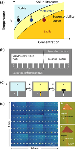
Goto et al [Citation141] proposed a method for directly forming organic single-crystal thin films with substrate-patterning features using solution-based growth. Their approach is affected by the nature of solubility. As depicted in figure (a), the state of the solution changes from unsaturated and stable to supersaturated upon reduction in temperature and/or increase in solution concentration. Spontaneous crystallization in solution can only occur in the supersaturated region and not in the stable zone. Crystal growth but not nucleation can proceed in the metastable zone, located between the solubility and supersolubility curves. The substrate is patterned into hydrophilic and hydrophobic regions (figures (a)–(c)), including nucleation control and growth control regions. Evaporation starts when the solution droplet of 3,9-bis(4-ethylphenyl)-peri-xanthenoxanthene (C2Ph-PXX) is confined in a hydrophilic surface. In the nucleation control region, the state of the solution changed from stable and unsaturated to supersaturated. In the growth control region, the state of the solution changes from stable to metastable. Thus, the solvent evaporates completely from the nucleation control region, and a crystalline film grows from a single stable nucleus within the growth control area. Figure (d) shows a cross-polarized optical microscopy image of C2Ph-PXX thin films grown by this method. All organic crystals have a typical pentagon shape, with similar facet angles of 82° to 98° in the designated locations. This solution-processed method is simple, efficient, and excellent in spatially separating the crystal nucleation and growth to achieve patterned single crystal arrays.
Figure 9 (a) Solubility–supersolubility diagram. (b) Micropattern with nucleation control region and growth control region. (c) Schematic of the growth model. (d) Cross-polarized microscopy image of C2Ph-PXX thin film arrays (left). Upper- and lower-right images show cross-polarized micrographs of the same thin film. The thin film has a typical pentagon shape with characteristic angles of 82° and 98°. (Reproduced with permission from [Citation141] © 2012 WILEY-VCH Verlag GmbH & Co. KGaA, Weinheim.)
Solution shearing
Introducing strain within the crystal lattice is a general method of increasing charge carrier mobility of inorganic materials. Accordingly, a solution-processed technique for organic semiconductors was proposed, wherein lattice strain is used to increase charge carrier mobility [Citation142, Citation143]. The π–π stacking distance or the spacing between cofacially stacked and conjugated backbones for organic semiconductors determines electron orbital overlap and mobility [Citation144]. They used a shearing plate that drags the TIPS-PEN solution across a heated substrate while maintaining the bulk of the solution between the plate and the substrate. The solution can only evaporate at the exposed front part. At a shearing speed of 0.4 mm s−1, oriented and millimeter-wide TIP-PEN crystals with lengths of ∼1 cm are obtained with the long axis parallel to the shearing direction. When the shearing speed is increased to 2.8 mm s−1, the organic crystals become narrower and shorter, and the carrier mobility increases. The highest value of 4.6 cm2 V−1 s−1 is achieved in the solution-sheared thin film at a speed of 2.8 mm s−1. The results of grazing incidence x-ray diffraction (GIXD) measurement revealed that the π–π stacking distance decreases with increasing shearing speed upon tuning the extent of lattice strain. However, further increasing the shearing speed decreases the mobility because of the formation of smaller and less-oriented crystallites (figure (c)). This technique provides more opportunities for the improvement of electrical properties of organic semiconductors. Although strain-induced organic crystals are metastable, they exhibit good chemical, thermal, and electrical stability. Upon combination with a pressure-assisted thermal cleavage, this solution shearing technique can also be applied to process higher rylene diimides with poor solubility [Citation145].
Figure 10 (a) (Left) schematic of the solution shearing method. (Right) cross-polarized microscopy image of solution-sheared TIPS-pentacene thin films formed via solution shearing. The black arrow represents the shearing direction. (b) Cross-polarized microscopy image of TIPS-pentacene sheared on 20 μm patterned line widths. The scale bar is 100 μm. (c) (Left) (101) and (010) d-spacing of TIPS-pentacene thin films sheared at different speeds. (Right) average and maximum charge carrier mobility of transistors fabricated from TIPS-pentacene thin films sheared at different speeds. (d) (Left) illustration of solution shearing using a micropillar-patterned blade. The arrow indicates the shearing direction. (Middle) scanning electron microscopy (SEM) image of a micropillar-patterned blade. Length scale = 50 μm. (Inset) top view of the micropillars under an optical microscope, with each pillar having a width of 35 μm and a height of 42 μm. (Right) streamline representation of simulated fluid flow around the micropillars. The arrow indicates the flow direction. The streamlines are color coded to indicate the scale of velocity (mm s−1), ranging from 0 (deep blue) to 1.3 mm s−1 (dark red). (e) Cross-polarized microscopy image of a TIPS-pentacene film coated from its mesitylene solution with (upper) and without (lower) using the FLUENCE technique. The white arrow denotes the shearing direction. (f) A photographic image of 1 mm-wide, 2 cm-long, single crystals on a Si wafer. (Reproduced with permission from [Citation143, Citation146, Citation147] © 2012 Nature Publishing Group, ©2013 WILEY-VCH Verlag GmbH & Co. KGaA, Weinheim and © 2013 Nature Publishing Group.)
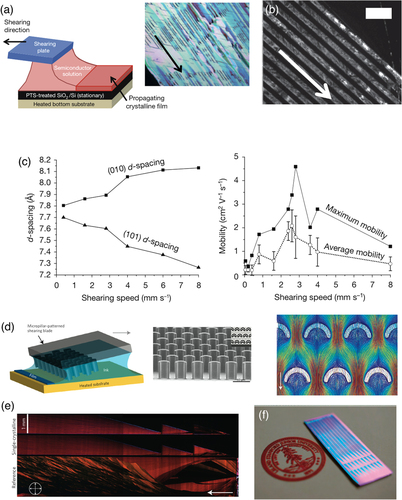
Further applications of this process lie in the combination with the surface wettability patterning technique. A previous study patterned the SiO2 substrate surface into fluorosilane-coated and -uncoated regions using photolithography [Citation146]. When the patterned line widths are as low as 2 μm or 0.5 μm, the thin films within the patterned regions exhibit more aligned crystalline domains compared with the nonpatterned substrate and substrates with 20 μm patterned line widths (figure (b)). The well-aligned organic crystalline domains stem from the improvement of the crystal texture and afford nucleation control.
Diao et al [Citation147] developed the fluid-enhanced crystal engineering (FLUENCE) technique, which can rapidly coat and pattern millimeter-wide, centimeter-long, and highly aligned monocrystalline organic semiconducting thin films. This technique, which yields unique solution-processed organic crystals, owes its success to two key factors. One is the printing blade with micropillar patterns (figure (d)). The pillar spacing is less than 100 μm, which induces rapid flow expansion following acceleration through the gap and thus facilitates lateral mass transport. The crescent-shaped cross-structure of the micropillars enhances flow separation from the micropillar surface. The shearing blade with micropillar arrays significantly improves the morphology of thin films comprising organic crystals. The other critical factor is the modulation of the contact line shape by patterning the substrate with solvent-wetted and dewetted regions. Figures (e) and (f) show the initial parts of the wetted region covered with triangular phenyltrichlorosilane (PTS), which is inspired by the coffee-ring effect. This triangular PTS controls the nucleation sites, facilitates nucleation anchoring, and eliminates twin boundary formation. Following the triangles is a series of narrow slits that control the growth of undesired crystallites. The resulting organic crystalline thin films in the patterned geometries can exhibit improvement in device performance with mobility values of up to 11 cm2 V−1 s−1. The FLUENCE technique is significantly instructive for future development in organic electronics toward low-cost, high-performance, and large devices. Further analyses reveal the crystallization mechanism using an in situ and real-time x-ray spectroscopy facility of microbeam grazing incidence wide-angle x-ray scattering (μGIWAXS) [Citation148]. The crystallization of small molecules takes place at the liquid–air interface forming a stable and regular crystalline phase, whereas the subsequent crystallization forms well-packed molecules underneath the stable ones exhibiting as nonequilibrium with enhanced charge carrier mobility by introducing greater electron orbital overlap between the semiconducting molecules.
Solution shearing and other similar methods that introduce lattice strain into organic crystals have been proven substantial and effective for the rapid growth of high-quality crystals. The remarkably enhanced device performance by strain-induced shortening of molecular packing with a very short distance of sub-angstrom scale can assure that organic semiconductors are comparable with polycrystalline silicon. Fundamental investigations, such as the formation mechanism of metastable crystals, crystallization process at the liquid–air and liquid–solid interfaces, and crystalline phases at these interfaces, are indispensable. Obviously, such studies are instructive for the further development in high-performance OFETs.
Other aspects with future perspectives
More on organic crystal growth from solutions
Recent studies have focused on organic-functioning crystals grown from solutions. New crystalline materials exhibiting high device performance in transistors have been merging into academic research. Knowledge of the driving force for crystallization in solutions is essential [Citation149], and further analyses are important to provide a better understanding of this field.
An organic crystal from solution is generally produced as a consequence of molecular aggregation for the formation of nuclei. These nuclei have the configurations that match the crystalline structure, which will eventually grow into crystals with large domain sizes. Factors such as solubility, supersaturation, diffusivity, and temperature affect the kinetics and mechanisms by which organic crystals are processed and formed in solutions. For instance, supersaturation regulates the number of molecules necessary to achieve an effective nucleating cluster, that is, the probability of nucleation increases with supersaturation. However, nucleation is more demanding than crystal growth. In addition, some supersaturated regions support crystal growth, whereas some suppress such growth. Upon nucleation, nuclei grow into mature crystals; this stage is referred to as crystal growth. Crystal growth is governed by both internal and external factors. Internal factors such as the three-dimensional crystal structure and crystal defects will determine the nature and strength of the intermolecular interactions between the crystal surface and the solution. External factors such as temperature, supersaturation, solvent, and impurities will affect the interactions at the solid–liquid interface.
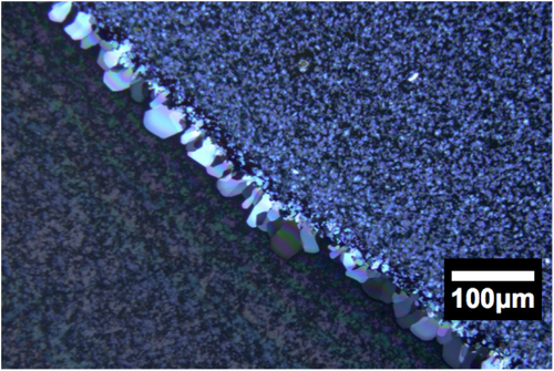
We have conducted a systematic analysis on the crystal growth via polymer-assisted solvent vapor annealing (PASVA) [Citation44]. Figure (a) shows a matrix of organic solvents and polymers that were used to probe the crystallization of C8-BTBT. We found that the crystallization of a small-molecule semiconductor via SVA correlates well with solvent miscibility and polymer-based films. Additional solvent absorbed on the polymer surface can enhance the molecular mobility on the substrate, allowing self-assembly in a distance of over hundreds of micrometers. Furthermore, the crystal growth mechanism follows the Ostwald ripening effect, that is, large crystals grow at the expense of small crystals as the large ones are more favored in terms of energy (figures (b) and (c)). The diffusion rate and crystal length increase with increasing PMMA thickness [Citation78]. Extremely long C8-BTBT crystals, 2.7 mm in length, were obtained based on the mechanism (figure (f)). Similarly, our recent experiments have shown that crystallization in a polymer-assisted system is interesting because the diffusion length is extremely long and the SVA crystallization process is different from other methods. Figure shows a clear, dark region in the cross-polarized microscopy image around the crystals from SVA. This region has a typical distance of tens of micrometers from the outer edge to the crystal, which is shorter than the diffusion length of small molecules. Within the dark region, the molecules that escaped from small crystals merge into a large one. Thus, investigations focused on the molecule behavior in this region can possibly reveal some interesting phenomena to clarify the crystallization mechanism of SVA.
Figure 11 (a) Cross-polarized microscopy images of vacuum-sublimed C8-BTBT films after SVA on different polymer base films; THF = tetrahydrofuran, PVP = polyvinylphenol, PαMS = α-methyl polystyrene. (b) Time-lapsed optical microscopy images of two crystals. (c) Length of crystals A and B in (b) and the average lengths of all the crystals as a function of time. (d) and (e) The diffusion rate at the early stage of crystal growth and the average crystal length as a function of PMMA thickness, respectively. (f) A crystal longer than 2 mm grown on a PMMA film via SVA. (Reproduced with permission from [Citation44] © 2012 The Royal Society of Chemistry.)
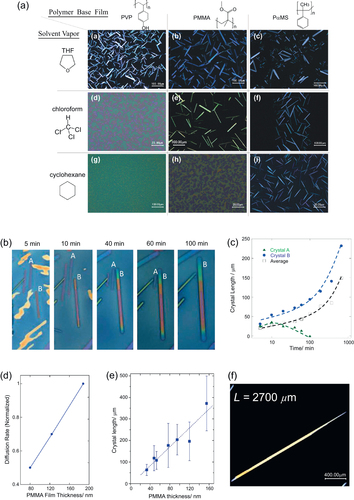
Figure 12 Crystals at the polymer–substrate interface after SVA.
External factors such as temperature and solvents can significantly change the external crystal morphology and charge transport because of the weak nature of van der Waals force as the main intermolecular force in organic crystals. For instance, C8-BTBT can form into rod-like crystals with sizes ranging from hundreds of micrometers to more than one millimeter via SVA. It can also be fabricated in plate-like shapes when directly spin-coated from polymer solutions. The mobility of C8-BTBT crystals also varies with different processing techniques based on the same device structure. When PCBM is spin-coated to amorphous thin films, typical n-type and ambipolar transistor behavior can be observed from OFETs [Citation150–Citation153]. By contrast, when PCBM is formed into large hexagonal crystals, electrical conduction is neither observed nor reported [Citation89, Citation154]. Elimination of electrical characteristics in PCBM crystals can be attributed to the addition of solvent molecules and the molecular packing that are unfavorable for charge transport.
Processing of organic crystals grown from solutions requires careful design and preparations to eliminate the influence of external factors. On the other hand, the distinct property of organic crystals stemming from their intrinsic properties also opens the way for controllable modifications at the molecular level. Some novel techniques have been used to fabricate high-performance organic crystal FETs from solution-based processes by inducing strain in organic molecular packing.
More on device physics of organic crystal FETs
The density of structural defects in the channel of organic crystal FETs is considerably lower than that of OFETs based on amorphous organic thin films. Thus, not only high device performance has been achieved and has room for further improvement, but FETs can also serve as an effective platform to study the intrinsic charge transport and interfacial property of organic semiconductors. In this subsection, we discuss the device physics of organic crystal FETs. Some works on vacuum-deposited crystals are also examined, which are instructive for solution-processed organic crystals. Other reviews are highly recommended for readers to obtain more comprehensive knowledge [Citation39, Citation96, Citation155, Citation156].
In-crystal and interface charge transport
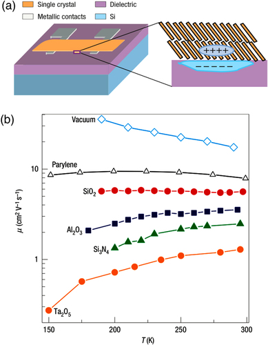
For an OFET with organic thin films in the amorphous or polycrystalline phase, results show that the conducting channel is positioned only within the first several molecular layers from the semiconductor/insulator interface [Citation157–Citation159]. Early experiments with rubrene single-crystal FETs also confirm the interfacial charge transport because the carrier mobility of rubrene crystal has shown a strong dependence on the dielectric constant of the gate insulator [Citation160]. Similarly, Takeya et al [Citation57] experimented on a rubrene single crystal. They observed a tuning of charge transport from in-crystal to the semiconductor/insulator interface by simply sweeping the gate voltage. They used a high-quality rubrene crystal with the highest charge carrier mobility because the length scale of the carrier distribution can be elongated in a weak electric field for a purified single crystal with nondoped intrinsic properties. A high mobility value of 5–25 cm2 V−1 s−1 was obtained in the low-gate voltage region, whereas a low mobility of 1–2 cm2 V−1 s−1 was observed as the typical value in the low-gate voltage region. The higher value of mobility is brought by the dilute distribution of the field-induced carriers into the crystal at the weak-gate electric field, whereas the decrease in mobility with increasing gate voltage occurs because the carriers are aggregated close to the interface.
The charge transport in an organic semiconducting crystal with the FET configuration is important to elucidate the intrinsic regime. As predicted, higher performance can be expected from the organic crystal FETs with charge transport in the bulk of the crystal, avoiding the reduction in mobility from scattering at the interface and the interaction with the gate dielectric.
Gate insulators and crystal interfaces
Materials science and engineering have been well established for applications in gate insulators in OFETs, including inorganic, polymeric dielectrics, and self-assembled mono- and multilayers [Citation161, Citation162]. In principle, the performance of OFETs depends greatly on the use of gate insulators [Citation6, Citation163]. The principal determinant factors of gate insulator over device performance include the surface roughness, interfacial defect density, chemical purity, and composition of materials. For instance, a V T shift upon prolonged gate bias stress can be caused by charge trapping at localized states in the gate insulator or at the semiconductor/insulator interface. Gate insulators also significantly affect the hysteresis behavior and reliability of OFETs. When a buffer layer of an apolar polymer insulator is introduced to a device structure, ambipolar characteristics can be observed even from the materials originally considered as p-type semiconductors [Citation164–Citation166].
In the case of organic semiconducting crystals as channel materials in OFETs, similar issues of gate insulator influences should also be carefully considered to achieve high performance. Works on organic crystal FETs are mostly based on the top-gate structure, wherein a gate insulating layer is deposited onto the crystal surfaces. Many attempts were unsuccessful because of damages to the fragile crystal surface during sputtering the metal oxides as dielectric. Using a polymer film of parylene as a gate insulator in organic crystal FETs improves performance because it is chemically inert with low surface density and because its deposition allows the organic crystals to remain at room temperature [Citation49]. Thus, damages to the crystal surface can be greatly minimized. Another method using a vacuum-gap as the gate insulating layer can increase the mobility from the organic single crystal surface [Citation55, Citation56, Citation167].
Aside from the technical points of the continuous improvement of device performance, gate insulator materials can also alter the charge transport behavior at the semiconducting crystal/insulator interface, which provides an understanding of carrier motion on a microscopic scale. The charge transport in polymer OFETs is dependent on dielectric polarizability [Citation165, Citation168]. Previous studies suggested that the randomly oriented dipoles present in the dielectric increase the disorder in the semiconducting channel. The more polar the dielectric, the larger the static dipolar disorder effect it produces in the polymer, thereby reducing the charge mobility. Hulea et al [Citation169] used a series of ionic insulating materials in OFETs based on rubrene sing crystals, in which the observation of intrinsic charge transport characteristics of the molecules is enabled because of the significant reduction in disorder (figure (a)). Figure (b) shows that the carrier mobility depends on the temperature, evolving from metallic-like to insulating-like with increasing dielectric constant of the insulator. The concept of interactions between charge carriers and the insulating layer is referred to as a 2D Fröhlich polaron model, in which the coupling of the polarization in the gate insulator and charge carrier is pictured as a quasi-particle termed in a ‘Fröhlich polaron’ [Citation8, Citation170–Citation172]. This work practically gives more credence to the deposition of ultra-thin organic buffer layers on the dielectric [Citation164].
Figure 13 (a) (Left) schematic of a rubrene single crystal FET. (Right) electrostatically induced holes moving at the dielectric–organic interface polarize the gate dielectric. A Fröhlich polaron can be formed as the hole and the induced charge move together due to sufficiently large coupling. (b) Temperature dependence of the carrier mobility in the rubrene single-crystal FET with six gate dielectrics, showing a continuous evolution from metallic-like to insulating-like, as the dielectric constant of the gate insulator is increased. (Reproduced with permission from [Citation169] © 2006 Nature Publishing Group.)
Technically, gate materials are important in the fabrication of functioning devices. For instance, the utilization of ferroelectric polymers can bring the devices into the application of memory transistors [Citation140, Citation173–Citation177]. The use of dielectrics comprising electrolytes, such as ionic liquids, ion gels, polymer electrolytes, and polyelectrolytes, can greatly reduce the operation voltage [Citation178–Citation184]. When considering the vertical phase separation during spin-coating from mixtures, the gate insulating and organic semiconducting layers can be fabricated directly with molecular smooth interface. This experiment has been well conducted using a blend of poly(3-hexylthiophene) (P3HT) and PMMA [Citation86], whereas solution-processed organic crystals have yet to be used as channel materials in a similar device.
Some observations of important scientific interest are associated with the influence of interfaces of organic crystals other than semiconductor/insulator interface. Most of them, from microscopic motion of charges, involve charge transfer behavior at the interfaces. One excellent demonstration is that the conductivity of rubrene crystals can be dramatically enhanced using surface modification of SAMs [Citation185]. Alves et al [Citation186] observed an interesting metallic conduction at the charge-transfer interface when a p-type organic crystal is placed onto the surface of an n-type crystal.
Contact resistance influences and calculation
Contact resistance in an OFET includes resistance at the metal/organic interface and access resistance from metal/semiconductor interface to the conducting channel. The first part owes mainly to the energy difference between the semiconducting band state and the work functions of electrode material; the other is determined by organic semiconductor thickness and device architecture. Contact resistance can reduce device performance in OFETs [Citation187–Citation197]. The four-probe method (4PM) is often used to discriminate the contact resistance from the channel resistance, extracting the intrinsic charge carrier mobility [Citation34, Citation55, Citation186, Citation198]. Contact resistance is also a critical factor of large variation in the performance of transistor arrays even on the same substrate. For organic crystals, when applying staggered device architectures (bottom-gate top-contact or top-gate bottom-contact), charge carriers are injected from the metal contact to the conducting channel at the direction that is basically not preferable for charge transport, leading to a relatively large value of contact resistance. Crystals often have larger variations in thickness than thin films; thus, uniformity in performance is frequently a critical consideration for future development and applications of OFETs based on semiconducting crystals. Improved device performance and uniformity have been achieved with the use of coplanar structures (bottom-gate bottom-contact or top-gate top-contact) [Citation70]. However, issues around considerations of the effective charge injection area still exist [Citation188, Citation193]. For instance, the coplanar architecture normally has a small charge injection/extraction area at the semiconductor/metal contact; meanwhile, charge injection/extraction can occur over the entire contact area in the staggered architecture, including the top and bottom surfaces [Citation192].
Inserting a chemically doped layer between the metal and organic semiconductor can effectively reduce contact resistance [Citation117, Citation199–Citation201]. However, doping into the active materials reaching the channel is difficult for organic semiconducting crystals because the molecules are highly ordered. Most organic crystal FETs reported in the literature, even when a layer is inserted to enhance charge injection, suffer from serious influences of the contact effect, appearing as the superlinear behavior in output characteristics at the low-drain-voltage region. Large contact resistance can also consume additional power because of Joule heating [Citation190].
Future works for reducing contact resistance in organic crystal FETs is of great importance. Quantitative calculation of the contact resistance in organic crystal transistors is likewise necessary. Both the transmission line method (TLM) and 4PM require complex electrode patterning to realize multiple channels or the four-terminal configuration. However, neither is applicable for organic crystal FETs because of the difficulty in preparing a crystal large enough to fabricate device patterns for the TLM or 4PM. To evaluate contact effects, we present the Y function method applied on organic crystal FETs [Citation68]. This method was established for silicon-based metal–oxide–semiconductor field-effect transistors and applied in organic thin film transistors to estimate contact resistance and low-field mobility (μ 0) from individual devices [Citation202, Citation203]. For our organic crystal FETs, the value of μ FET extracted from the saturation regime is lower than that of μ 0 and generally decreases with increasing contact resistance.
More than patterning
Although organic semiconducting crystals can yield high transistor performance from their highly ordered molecular packing, two critical techniques have to be developed to move organic crystal transistors from research topics in laboratories into practical products in markets. One is the patterning technology for the deposition and growth of organic crystals at the desired regions. Many demonstrations discussed in this review confirmed that the patterning methods hold great capability in fabricating OFET arrays based on solution-processed organic crystals. The other prerequisite is the well-controlled orientation and alignment of organic crystals. Organic crystal FETs frequently experience poor uniformity in device performance (section 2.2.2). Variation in performance of organic crystal FETs is mainly caused by two factors. One is crystal morphology; crystal thickness determines the access resistance from the metal contact to the conducting channel in a staggered device structure (bottom-gate top-contact or top-gate bottom-contact). The metal contact quality in transistors can result in performance variations. Organic semiconductors deposited as crystalline thin films are preferable from this point of view [Citation23]. The other factor is the orientation and alignment of crystals, which introduce anisotropy of charge transport and differences in the width and length of the active channels. For instance, when rod-like semiconducting crystals with favorable charge transport along the long crystal axis are used, the channel width (W) and length (L) are the width and length of the crystals that bridge the source and drain electrode, respectively. Hence, orientation and alignment influence the uniformity in performance and should be carefully considered.
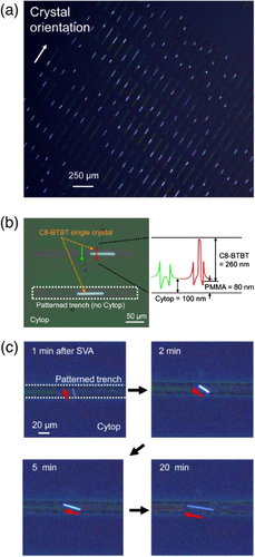
Some depositing techniques from solutions, such as zone casting [Citation32], doctor blading [Citation204, Citation205], brush painting [Citation206], and solution shearing [Citation143, Citation146, Citation147], exhibit intrinsic capability in aligning the organic molecules and forming well-oriented crystals. However, a certain distribution still exists in organic aligning directions. Similarly, alignment of solution-processed organic crystals can be obtained in a hundred-micrometer scale when using a stamp with confining structure [Citation207] or applying a small solution-pinning wafer on substrate [Citation41, Citation42]. A solution-based method of PASVA that we proposed can produce organic single crystals with well-controlled orientation (figure (a)) [Citation208]. CYTOP was spin-coated onto the SiO2 substrate and then patterned into a series of narrow wettable trenches using lithography. An optimal trench width of 20 μm can produce organic crystals (C8-BTBT) with [Citation100] crystal direction well aligned along the long axis of the rectangular trench (figure (b)). The driving forces of the self-organization of organic crystals are the self-assembly of C8-BTBT molecules on the soluble polymer base film and the geometric influence of the confinement area on the crystal alignment (figure (c)).
Figure 14 (a) Cross-polarized optical micrograph of an organic single crystal array. (b) Organic single crystals fabricated by the present method. The polarized optical micrograph shows that the crystals are fabricated only in the trenches and have the same crystal orientation. The surface profile shows that the typical thickness of the crystals is approximately 250 nm. (c) Real-time observation of the crystal growth and alignment. (Reproduced with permission from [Citation208] © 2012 Authors.)
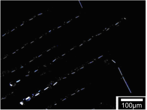
However, a deposition process that solely realizes patterning or orientation is still unsatisfactory for the benchmarks of industrial products. Future research should focus on the development of solution-processed techniques that can simultaneously pattern and orient organic crystals. We propose a method using PASVA performed on a patterned substrate surface with hydrophobic, highly hydrophilic, and weakly hydrophilic regions. Figure shows a typical cross-polarized microscopy image of the resulting rod-like crystal arrays with well-controlled alignment. This project is currently under further investigation in our group.
Figure 15 Cross-polarized microscopy image showing the recent progress of fabricating well-aligned organic single crystals in patterned regions.
Conclusions
In this review, we examined typical techniques, providing up-to-date knowledge of the patterning technology for solution-processed organic crystals and their applications in OFETs. Our recent research work on the spin-coating process from mixture solutions for the growth of patterned organic crystals was introduced. In addition, some key issues for the further development in this research topic, such as the organic crystal growth from solutions, device physics of organic crystal FETs, and patterning the crystals with controllable alignment, were also discussed.
Acknowledgements
We would like to express our appreciation to Dr Koichi Ikeda from Nippon Kayaku for providing C8-BTBT. Also, we would like to thank Prof. Kazuo Takimiya for fruitful discussions. This study is supported partially by NSFC under grant no. 61306021, NSFJS under grant nos. BK20130579, KB2011011, and BK20130055, and 973 project under grant nos. 2013CBA01600 and 2013CB932900.
References
- CicoiraFSantatoC 2013 Organic Electronics Weinheim Wiley-VCH
- KlaukH 2006 Organic Electronics Weinheim Wiley-VCH
- GrasserTMellerG 2009 Organic Electronics Berlin-Heidelberg Springer
- DeenM JKlaukH 2010 Organic Semiconductor Materials, Devices, and Processing 2 Pennington, NJ The Electrochemical Society
- KawaseTShimodaTNewsomeCSirringhausHFriendR H 2003 Thin Solid Films 438-439 279 287 279–87 10.1016/S0040-6090(03)00801-0
- SirringhausH 2005 Adv. Mater. 17 2411 2425 2411–25 10.1002/(ISSN)1521-4095
- TesslerNPreezantYRappaportNRoichmanY 2009 Adv. Mater. 21 2741 2761 2741–61 10.1002/adma.200803541
- CoropceanuVCornilJda Silva FilhoD AOlivierYSilbeyRBrédasJ-L 2007 Chem. Rev. 107 926 952 926–52 10.1021/cr050140x
- Muller-HorscheEHaarerDScherH 1987 Phys. Rev. B 35 1273 10.1103/PhysRevB.35.1273
- ScherHMontrollE W 1975 Phys. Rev. B 12 2455 10.1103/PhysRevB.12.2455
- BaoZGundlachD J 2005 Organic Field-Effect Transistors, Proc. SPIE vol 6658 (Bellingham, WA: SPIE)
- BaoZLocklinJ 2007 Organic Field-Effect Transistors Boca Raton, FL CRC
- LiF MNathanAWuY LOngB S 2011 Organic Thin Film Transistor Integration: A Hybnd Approach Weinheim Wiley-VCH
- LeeSKooBParkJ-GMoonHHahnJKimJ M 2006 MRS Bulletin 31 455 459 455–9 10.1557/mrs2006.118
- EbisawaFKurokawaTNaraS 1983 J. Appl. Phys. 54 3255 10.1063/1.332488
- TsumuraAKoezukaHAndoT 1986 Appl. Phys. Lett. 49 1210 10.1063/1.97417
- AssadiASvenssonCWillanderMInganäsO 1988 Appl. Phys. Lett. 53 195 10.1063/1.100171
- HorowitzGFichouDPengXXuZGarnierF 1989 Solid State Commun. 72 381 384 381–4 10.1016/0038-1098(89)90121-X
- KudoKYamashinaMMoriizumiT 1984 Jpn J. Appl. Phys. 23 130 10.1143/JJAP.23.130
- DimitrakopoulosC DMalenfantP R 2002 Adv. Mater. 14 99 117 99–117 10.1002/(ISSN)1521-4095
- HorowitzG 2003 Adv. Funct. Mater. 13 53 60 53–60 10.1002/adfm.200390006
- CampbellI HSmithD L 2001 Solid State Phys. 55 1 117 1–117 10.1016/S0081-1947(01)80003-5
- LiYLiuCKumataniADarmawanPMinariTTsukagoshiK 2011 Org. Electron. 13 264 272 264–72 10.1016/j.orgel.2011.11.012
- LiYLiuCXuYMinariTDarmawanPTsukagoshiK 2012 Org. Electron. 13 815 819 815–9 10.1016/j.orgel.2011.11.012
- LeeS SKimC SGomezE DPurushothamanBToneyM FWangCHexemerAAnthonyJ ELooY-L 2009 Adv. Mater. 21 3605 3609 3605–9 10.1002/adma.v21:35
- LiuSWangW MBrisenoA LMannsfeldS C BBaoZ 2009 Adv. Mater. 21 1217 1232 1217–32 10.1002/adma.v21:12
- YamaoTMikiTAkagamiHNishimotoYOtaSHottaS 2007 Chem. Mater. 19 3748 3753 3748–53 10.1021/cm071051z
- WangCDongHHuWLiuYZhuD 2012 Chem. Rev. 112 2208 2267 2208–67 10.1021/cr100380z
- MannsfeldS CShareiALiuSRobertsM EMcCullochIHeeneyMBaoZ 2008 Adv. Mater. 20 4044 4048 4044–8 10.1002/adma.v20:21
- RobertsM EMannsfeldS C BStoltenbergR MBaoZ 2009 Org. Electron. 10 377 383 377–83 10.1016/j.orgel.2008.12.001
- SoedaJOkamotoTHamaguchiAIkedaYSatoHYamanoATakeyaJ 2013 Org. Electron. 14 1211 1217 1211–7 10.1016/j.orgel.2013.01.004
- PisulaWMenonAStepputatMLieberwirthIKolbUTraczASirringhausHPakulaTMüllenK 2005 Adv. Mater. 17 684 689 684–9 10.1002/(ISSN)1521-4095
- ReeseCBaoZ 2007 Mater. Today 10 20 27 20–7 10.1016/S1369-7021(07)70016-0
- NakayamaK 2011 Adv. Mater. 23 1626 1629 1626–9 10.1002/adma.201004387
- NaabB DHimmelbergerSDiaoYVandewalKWeiPLussemBSalleoABaoZ 2013 Adv. Mater. 25 4663 4667 4663–7 10.1002/adma.v25.33
- MinemawariHYamadaTMatsuiHTsutsumiJHaasSChibaRKumaiRHasegawaT 2012 Nature 475 364 367 364–7 10.1038/nature10313
- MannsfeldS C BLocklinJReeseCRobertsM ELovingerA JBaoZ 2007 Adv. Funct. Mater. 17 1617 1622 1617–22 10.1002/adfm.200600865
- AkkermanH BLiHBaoZ 2012 Org. Electron. 13 2056 2062 2056–62 10.1016/j.orgel.2012.06.019
- de BoerR W IGershensonM EMorpurgoA FPodzorovV 2004 Phys. Stat. Sol. (a) 201 1302 1331 1302–31 10.1002/(ISSN)1521-396X
- BrisenoA LAizenbergJHanY-JPenkalaR AMoonHLovingerA JKlocCBaoZ 2005 J. Am. Chem. Soc. 127 12164 12165 12164–5 10.1021/ja052919u
- LiHTeeB C-KChaJ JCuiYChungJ WLeeS YBaoZ 2012 J. Am. Chem. Soc. 134 2760 2765 2760–5 10.1021/ja210430b
- LiHTeeB C-KGiriGChungJ WLeeS YBaoZ 2012 Adv. Mater. 24 2588 2591 2588–91 10.1002/adma.v24.19
- LiuCMinariTLuXKumataniATakimiyaKTsukagoshiK 2010 Adv. Mater. 23 523 526 523–6 10.1002/adma.v23.4
- LiuCMinariTLiYKumataniALeeM VAthena PanS HTakimiyaKTsukagoshiK 2012 J. Mater. Chem. 22 8462 10.1039/c2jm15747k
- LiuCLiYXuYMinariTLiSTakimiyaKTsukagoshiK 2012 Org. Electron. 13 2975 2984 2975–84 10.1016/j.orgel.2012.08.024
- LimJ ALiuFFerdousSMuthukumarMBrisenoA L 2010 Mater. Today 13 14 24 14–24 10.1016/S1369-7021(10)70080-8
- PopeMSwenbergC E 1999 Electronic Processes in Organic Crystals and Polymers USA Oxford University Press
- HallamTLeeMZhaoNNandhakumarIKemerinkMHeeneyMMcCullochISirringhausH 2009 Phys. Rev. Lett. 103 256803 10.1103/PhysRevLett.103.256803
- PodzorovVPudalovV MGershensonM E 2003 Appl. Phys. Lett. 82 1739 10.1063/1.1560869
- TakeyaJGoldmannCHaasSPernstichK PKettererBBatloggB 2003 J. Appl. Phys. 94 5800 10.1063/1.1618919
- ButkoV YChiXLangD VRamirezA P 2003 Appl. Phys. Lett. 83 4773 10.1063/1.1631736
- PodzorovVSysoevS ELoginovaEPudalovV MGershensonM E 2003 Appl. Phys. Lett. 83 3504 10.1063/1.1622799
- de BoerR W IKlapwijkT MMorpurgoA F 2003 Appl. Phys. Lett. 83 4345 10.1063/1.1629144
- ButkoV YChiXRamirezA P 2003 Solid State Commun. 128 431 434 431–4 10.1016/j.ssc.2003.08.041
- SundarV C 2004 Science 303 1644 1646 1644–6 10.1126/science.1094196
- MenardEPodzorovVHurS HGaurAGershensonM ERogersJ A 2004 Adv. Mater. 16 2097 2101 2097–101 10.1002/(ISSN)1521-4095
- TakeyaJ 2007 Phys. Rev. Lett. 98 196804 10.1103/PhysRevLett.98.196804
- JurchescuO DPopinciucMvan WeesB JPalstraT T M 2007 Adv. Mater. 19 688 692 688–92 10.1002/(ISSN)1521-4095
- ParkS YKwonTLeeH H 2006 Adv. Mater. 18 1861 1864 1861–4 10.1002/(ISSN)1521-4095
- MannsfeldS CBrisenoA LLiuSReeseCRobertsM EBaoZ 2007 Adv. Funct. Mater. 17 3545 3553 3545–53 10.1002/(ISSN)1616-3028
- MinariTLiuCKanoMTsukagoshiK 2011 Adv. Mater. 24 299 306 299–306 10.1002/adma.201102554
- BrisenoA LMannsfeldS C BLingM MLiuSTsengR JReeseCRobertsM EYangYWudlFBaoZ 2006 Nature 444 913 917 913–7 10.1038/nature05427
- CavalliniM 2005 Nano Lett. 5 2422 2425 2422–5 10.1021/nl051685+
- DimitrakopoulosC DMascaroD J 2001 IBM J. Res. Dev. 45 11 27 11–27 10.1147/rd.451.0011
- RuizR 2004 Chem. Mater. 16 4497 4508 4497–508 10.1021/cm049563q
- LiuSBecerrilH ALeMieuxM CWangW MOhJ HBaoZ 2009 Adv. Mater. 21 1266 1270 1266–70 10.1002/adma.v21:12
- LiuYLiHTuDJiZWangCTangQLiuMHuWLiuYZhuD 2006 J. Am. Chem. Soc. 128 12917 12922 12917–22 10.1021/ja0636183
- LiYLiuCKumataniADarmawanPMinariTTsukagoshiK 2011 AIP Advances 1 022149 10.1063/1.3630128
- MinariTKanoMMiyaderaTWangS-DAoyagiYTsukagoshiK 2009 Appl. Phys. Lett. 94 093307 10.1063/1.3095665
- LiYLiuCKumataniADarmawanPMinariTTsukagoshiK 2012 Mol. Cryst. Liq. Cryst. 566 13 17 13–17 10.1080/15421406.2012.703812
- KanoMMinariTTsukagoshiK 2010 Appl. Phys. Express 3 051601 10.1143/APEX.3.051601
- MinariTKanoMMiyaderaTWangS-DAoyagiYSetoMNemotoTIsodaSTsukagoshiK 2008 Appl. Phys. Lett. 92 173301 10.1063/1.2912822
- KimS HChoiDChungD SYangCJangJParkC EParkS-H K 2008 Appl. Phys. Lett. 93 113306 10.1063/1.2979691
- ChoiDAhnBKimS HHongKReeMParkC E 2012 ACS Appl. Mater. Interfaces 4 117 122 117–22 10.1021/am201074n
- LiuCLiYLeeM VKumataniATsukagoshiK 2013 Phys. Chem. Chem. Phys. 15 7917 7933 7917–33 10.1039/c3cp44715d
- LiuCLiYMinariTTakimiyaKTsukagoshiK 2012 Org. Electron. 13 1146 1151 1146–51 10.1016/j.orgel.2012.08.024
- IwatsuFKobayashiTUyedaN 1980 J. Phys. Chem. 84 3223 3230 3223–30 10.1021/j100461a018
- MascaroD JThompsonM ESmithH IBulovic´V 2005 Org. Electron. 6 211 220 211–20 10.1016/j.orgel.2005.07.001
- ToffoloFBrinkmannMGrecoOBiscariniFTalianiCGomesH LAielloIGhediniM 1999 Synthetic Met. 101 140 141 140–1 10.1016/S0379-6779(98)01415-5
- BrinkmannMWittmannJ CChaumontCAndreJ J 1997 Thin Solid Films 292 192 203 192–203 10.1016/S0040-6090(96)09087-6
- GundlachD JJacksonT NSchlomD GNelsonS F 1999 Appl. Phys. Lett. 74 3302 10.1063/1.123325
- LiuYShiQDongHTanJHuWZhanX 2012 Org. Electron. 13 2372 2378 2372–8 10.1016/j.orgel.2012.08.024
- XuZChenL-MYangGHuangC-HHouJWuYLiGHsuC-SYangY 2009 Adv. Funct. Mater. 19 1227 1234 1227–34 10.1002/adfm.v19:8
- FelicissimoM PJarzabDGorgoiMForsterMScherfUScharberM CSvenssonSRudolfPLoiM A 2009 J. Mater. Chem. 19 4899 10.1039/b906297a
- AnselmoA SLindgrenLRyszJBernasikABudkowskiAAnderssonM RSvenssonKVan StamJMoonsE 2011 Chem. Mater. 23 2295 2302 2295–302 10.1021/cm1021596
- QiuLLimJ AWangXLeeW HHwangMChoK 2008 Adv. Mater. 20 1141 1145 1141–5 10.1002/adma.v20:6
- BjörströmC MNilssonSBernasikABudkowskiAAnderssonMMagnussonK OMoonsE 2007 Appl. Surf. Sci. 253 3906 3912 3906–12 10.1016/j.apsusc.2006.08.024
- SirringhausH 2009 Adv. Mater. 21 3859 3873 3859–73 10.1002/adma.v21:38/39
- ColleRGrossoGRonzaniAGazzanoMPalermoV 2012 Carbon 50 1332 1337 1332–7 10.1016/j.carbon.2011.11.003
- FraboniBFemoniCMencarelliISettiLDi PietroRCavalliniAFraleoni-MorgeraA 2009 Adv. Mater. 21 1835 1839 1835–9 10.1002/adma.v21:18
- EbataHIzawaTMiyazakiETakimiyaKIkedaMKuwabaraHYuiT 2007 J. Am. Chem. Soc. 129 15732 15733 15732–3 10.1021/ja074841i
- JiangLHuWWeiZXuWMengH 2009 Adv. Mater. 21 3649 3653 3649–53 10.1002/adma.v21:36
- TangQ QLiH HLiuY YHuW W 2006 J. Am. Chem. Soc. 128 14634 14639 14634–9 10.1021/ja064476f
- WangCLiuYWeiZLiHXuWHuW 2010 Appl. Phys. Lett. 96 143302 10.1063/1.3378268
- WeiZ 2010 Adv. Mater. 22 2458 2462 2458–62 10.1002/adma.v22:22
- HasegawaTTakeyaJ 2009 Sci. Technol. Adv. Mater. 10 024314 10.1088/1468-6996/10/2/024314
- LeeH MMoonHKimH-SKimY NChoiS-MYooSChoS O 2011 Org. Electron. 12 1446 1453 1446–53 10.1016/j.orgel.2011.05.015
- ForrestS R 2004 Nature 428 911 918 911–8 10.1038/nature02498
- RogersJ ABaoZBaldwinKDodabalapurACroneBRajuV RKuckVKatzHAmundsonKEwingJ 2001 Proc. Natl Acad. Sci. USA 98 4835 4840 4835–40 10.1073/pnas.091588098
- ZschieschangUKlaukHHalikMSchmidGDehmC 2003 Adv. Mater. 15 1147 1151 1147–51 10.1002/adma.200305012
- SomeyaTKatoYSekitaniTIbaSNoguchiYMuraseYKawaguchiHSakuraiT 2005 Proc. Natl Acad. Sci. USA 102 12321 12325 12321–5 10.1073/pnas.0502392102
- SomeyaTSekitaniTIbaSKatoYKawaguchiHSakuraiT 2004 Proc. Natl Acad. Sci. USA 101 9966 9970 9966–70 10.1073/pnas.0401918101
- SekitaniTZschieschangUKlaukHSomeyaT 2010 Nat. Mater. 9 1015 1022 1015–22 10.1038/nmat2896
- LiYLiuCWangYYangYWangXShiYTsukagoshiK 2013 AIP Advances 3 052123 10.1063/1.4811370
- TobjörkDÖsterbackaR 2011 Adv. Mater. 23 1935 1961 1935–61 10.1002/adma.201004692
- KimY HMoonD GHanJ I 2004 IEEE Electron. Device Lett. 25 702 704 702–4 10.1109/LED.2004.836502
- BollströmRMäättänenATobjörkDIhalainenPKaihovirtaNÖsterbackaRPeltonenJToivakkaM 2009 Organic Electronics 10 1020 1023 1020–3 10.1016/j.orgel.2009.04.014
- EderFKlaukHHalikMZschieschangUSchmidGDehmC 2004 Appl. Phys. Lett. 84 2673 10.1063/1.1690870
- YoonBShinHYarimagaOHamD-YKimJParkI SKimJ-M 2012 J. Mater. Chem. 22 8680 10.1039/c2jm30301a
- WangXSumbojaAFooW LYanC YTsukagoshiKLeeP S 2013 RSC Adv. 3 15827 15833 15827–33 10.1039/c3ra41807c
- KhanM ABhansaliU SAlshareefH N 2012 Adv. Mater. 24 2165 2170 2165–70 10.1002/adma.201200626
- MannerbroRRanlöfMRobinsonNForchheimerR 2008 Synthetic Met. 158 556 560 556–60 10.1016/j.synthmet.2008.03.030
- NogiMKomodaNOtsukaKSuganumaK 2013 Nanoscale 5 4395 10.1039/c3nr00231d
- YoonBShinHKangE-MChoD WShinKChungHLeeC WKimJ-M 2013 ACS Appl. Mater. Interfaces 5 4527 4535 4527–35 10.1021/am303300g
- ZschieschangUYamamotoTTakimiyaKKuwabaraHIkedaMSekitaniTSomeyaTKlaukH 2010 Adv. Mater. 23 654 658 654–8 10.1002/adma.201003374
- AnderssonPNilssonDSvenssonP OChenMMalmströmARemonenTKuglerTBerggrenM 2002 Adv. Mater. 14 1460 1464 1460–4 10.1002/1521-4095(20021016)14:20<1460::AID-ADMA1460>3.0.CO;2-S
- MinariTDarmawanPLiuCLiYXuYTsukagoshiK 2012 Appl. Phys. Lett. 100 093303 10.1063/1.3690949
- OheTKuribayashiMYasudaRTsuboiANomotoKSatoriKItabashiMKasaharaJ 2008 Appl. Phys. Lett. 93 053303 10.1063/1.2966350
- QuirkMSerdaJ 2001 Semiconductor Manufacturing Technology New York Prentice Hall
- SalzmanR FXueJRandB PAlexanderAThompsonM EForrestS R 2005 Org. Electron. 6 242 246 242–6 10.1016/j.orgel.2005.09.001
- HeggieD AMacDonaldB LHillI G 2006 J. Appl. Phys. 100 104505 10.1063/1.2374694
- JakobssonFCrispinXBerggrenM 2009 Org. Electron. 10 95 106 95–106 10.1016/j.orgel.2008.10.006
- JurchescuO DBaasJPalstraT T M 2004 Appl. Phys. Lett. 84 3061 10.1063/1.1704874
- LiYLiuCLeeM VXuYWangXShiYTsukagoshiK 2012 J. Mater. Chem. C 1 1352 10.1039/c2tc00384h
- SirringhausH 2000 Science 290 2123 2126 2123–6 10.1126/science.290.5499.2123
- KimY-HParkS K 2011 J. Inform. Disp. 12 199 203 199–203 10.1080/15980316.2011.621309
- KjellanderB K CSmaalW T TMynyKGenoeJDehaeneWHeremansPGelinckG H 2013 Org. Electron. 14 768 774 768–74 10.1016/j.orgel.2012.12.027
- ChoS YKoJ MLimJLeeJ YLeeC 2013 J. Mater. Chem. C 1 914 10.1039/c2tc00360k
- LeeM WRyuG SLeeY UPearsonCPettyM CSongC K 2012 Microelectron. Eng. 95 1 4 1–4 10.1016/j.mee.2012.01.006
- IhnenA CPetrockA MChouTSamuelsP JFuchsB ELeeW Y 2011 Appl. Surf. Sci. 258 827 833 827–33 10.1016/j.apsusc.2011.08.125
- LimJ ALeeW HLeeH SLeeJ HParkY DChoK 2008 Adv. Funct. Mater. 18 229 234 229–34 10.1002/(ISSN)1616-3028
- KominoTKuwabaraHIkedaMYahiroMTakimiyaKAdachiC 2013 Langmuir 29 9592 9597 9592–7 10.1021/la401729k
- LiX 2011 Org. Electron. 12 1319 1327 1319–27 10.1016/j.orgel.2011.04.020
- KjellanderB K CSmaalW T TAnthonyJ EGelinckG H 2010 Adv. Mater. 22 4612 4616 4612–6 10.1002/adma.201001697
- CalvertP 2001 Chem. Mater. 13 3299 3305 3299–305 10.1021/cm0101632
- SirringhausHShimodaT 2003 MRS Bulletin 28 802 806 802–6 10.1557/mrs2003.228
- BurnsS ECainPMillsJWangJSirringhausH 2003 MRS Bulletin 28 829 834 829–34 10.1557/mrs2003.232
- de GansB JDuineveldP CSchubertU S 2004 Adv. Mater. 16 203 213 203–13 10.1002/(ISSN)1521-4095
- SinghMHaverinenH MDhagatPJabbourG E 2010 Adv. Mater. 22 673 685 673–85 10.1002/adma.v22:6
- KangS JBaeIParkY JParkT HSungJYoonS CKimK HChoiD HParkC 2009 Adv. Funct. Mater. 19 1609 1616 1609–16 10.1002/adfm.v19:10
- GotoOTomiyaSMurakamiYShinozakiATodaAKasaharaJHobaraD 2012 Adv. Mater. 24 1117 1122 1117–22 10.1002/adma.v24.8
- BecerrilH ARobertsM ELiuZLocklinJBaoZ 2008 Adv. Mater. 20 2588 2594 2588–94 10.1002/adma.v20:13
- GiriGVerploegenEMannsfeldS C BAtahan-EvrenkSKimDo HwanLeeS YBecerrilH AAspuru-GuzikAToneyM FBaoZ 2012 Nature 480 504 508 504–8 10.1038/nature10683
- BrédasJ LCalbertJ Pda Silva FilhoD ACornilJ 2002 Proc. Natl Acad. Sci. USA 99 5804 5809 5804–9 10.1073/pnas.092143399
- OhJ HLeeW-YNoeTChenW-CKönemannMBaoZ 2011 J. Am. Chem. Soc. 133 4204 4207 4204–7 10.1021/ja110486s
- GiriGParkSVosgueritchianMShulakerM MBaoZ 2013 Adv. Mater. 26 487 493 487–93 10.1002/adma.201302439
- DiaoY 2013 Nat. Mater. 12 665 671 665–71 10.1038/nmat3650
- SmilgiesD MLiRGiriGChouK W 2013 Phys. Status Solidi (RRL) 7 177 179 177–9 10.1002/pssr.201206507
- Rodríguez-HornedoN RMurphyD 1999 J. Pharm. Sci. 88 651 660 651–60 10.1002/(ISSN)1520-6017
- ShkunovMSimmsRHeeneyMTierneySMcCullochI 2005 Adv. Mater. 17 2608 2612 2608–12 10.1002/(ISSN)1521-4095
- ChikamatsuMNagamatsuSYoshidaYSaitoKYaseKKikuchiK 2005 Appl. Phys. Lett. 87 203504 10.1063/1.2130712
- TiwariS PZhangX-HPotscavageW JKippelenB 2009 J. Appl. Phys. 106 054504 10.1063/1.3204655
- AnthopoulosT DTanaseCSetayeshSMeijerE JHummelenJ CBlomP W Mde LeeuwD M 2004 Adv. Mater. 16 2174 2179 2174–9 10.1002/(ISSN)1521-4095
- DabirianRFengXOrtolaniLLiscioAMorandiVMüllenKSamorìPPalermoV 2010 Phys. Chem. Chem. Phys. 12 4473 10.1039/b923496a
- GershensonM EPodzorovV 2006 Rev. Mod. Phys. 78 973 989 973–89 10.1103/RevModPhys.78.973
- BrooksJ S 2010 Chem. Soc. Rev. 39 2667 2694 2667–94 10.1039/b913417b
- TelloMChiesaMDuffyC MSirringhausH 2008 Adv. Funct. Mater. 18 3907 3913 3907–13 10.1002/adfm.v18:24
- GranstromE LFrisbieC D 1999 J. Phys. Chem. B 103 8842 8849 8842–9 10.1021/jp991460l
- DinelliFMurgiaMLevyPCavalliniMBiscariniFde LeeuwD 2004 Phys. Rev. Lett. 92 116802 10.1103/PhysRevLett.92.116802
- StassenA Fde BoerRIosadN NMorpurgoA F 2004 Appl. Phys. Lett. 85 3899 3901 3899–901 10.1063/1.1812368
- FacchettiAYoonM HMarksT J 2005 Adv. Mater. 17 1705 1725 1705–25 10.1002/(ISSN)1521-4095
- VeresJOgierSLloydGde LeeuwD 2004 Chem. Mater. 16 4543 4555 4543–55 10.1021/cm049598q
- LeeBWanAMastrogiovanniDAnthonyJ EGarfunkelEPodzorovV 2010 Phys. Rev. B 82 085302 10.1103/PhysRevB.82.014104
- ChuaL-LZaumseilJChangJ-FOuE C-WHoP K HSirringhausHFriendR H 2005 Nature 434 194 199 194–9 10.1038/nature03376
- CornilJBrédasJ LZaumseilJSirringhausH 2007 Adv. Mater. 19 1791 1799 1791–9 10.1002/(ISSN)1521-4095
- ZaumseilJDonleyC LKimJ SFriendR HSirringhausH 2006 Adv. Mater. 18 2708 2712 2708–12 10.1002/(ISSN)1521-4095
- UnoMUemuraTKanaokaYChenZFacchettiATakeyaJ 2013 Org. Electron. 14 1656 1662 1656–62 10.1016/j.orgel.2013.03.009
- VeresJOgierS DLeemingS WCupertinoD CMohialdin KhaffafS 2003 Adv. Funct. Mater. 13 199 204 199–204 10.1002/adfm.200390030
- HuleaI NFratiniSXieHMulderC LIossadN NRastelliGCiuchiSMorpurgoA F 2006 Nat. Mater. 5 982 986 982–6 10.1038/nmat1774
- FröhlichHPelzerHZienauS 1950 Philos. Mag. 41 221 242 221–42 10.1080/14786445008521794
- KirovaNBussacM N 2003 Phys. Rev. B 68 235312 10.1103/PhysRevB.68.235312
- DevreeseJ TAlexandrovA S 2009 Rep. Prog. Phys. 72 066501 10.1088/0034-4885/72/6/066501
- HoriuchiSTokuraY 2008 Nat. Mater. 7 357 366 357–66 10.1038/nmat2137
- NaberR C GBlomP W MGelinckG HMarsmanA Wde LeeuwD M 2005 Adv. Mater. 17 2692 2695 2692–5 10.1002/(ISSN)1521-4095
- NaberR C GTanaseCBlomP W MGelinckG HMarsmanA WTouwslagerF JSetayeshSde LeeuwD M 2005 Nat. Mater. 4 243 248 243–8 10.1038/nmat1329
- NaberR C GAsadiKBlomP W Mde LeeuwD Mde BoerB 2009 Adv. Mater. 22 933 945 933–45 10.1002/adma.200900759
- ZirklMStadloberBLeisingG 2007 Ferroelectrics 353 173 185 173–85 10.1080/00150190701368133
- ChoJ HLeeJXiaYKimBHeYRennM JLodgeT PDaniel FrisbieC 2008 Nat. Mater. 7 900 906 900–6 10.1038/nmat2291
- OnoSSekiSHiraharaRTominariYTakeyaJ 2008 Appl. Phys. Lett. 92 103313 10.1063/1.2898203
- TakeyaJYamadaKHaraKShigetoKTsukagoshiKIkehataSAoyagiY 2006 Appl. Phys. Lett. 88 112102 10.1063/1.2186513
- XiaYZhangWHaMChoJ HRennM JKimC HFrisbieC D 2010 Adv. Funct. Mater. 20 587 594 587–94 10.1002/adfm.v20:4
- HerlogssonLCölleMTierneySCrispinXBerggrenM 2010 Adv. Mater. 22 72 76 72–6 10.1002/adma.v22:1
- LuW 2002 Science 297 983 987 983–7 10.1126/science.1072651
- LarssonOSaidEBerggrenMCrispinX 2009 Adv. Funct. Mater. 19 3334 3341 3334–41 10.1002/adfm.v19:20
- CalhounM FSanchezJOlayaDGershensonM EPodzorovV 2007 Nat. Mater. 7 84 89 84–9 10.1038/nmat2059
- AlvesHMolinariA SXieHMorpurgoA F 2008 Nat. Mater. 7 574 580 574–80 10.1038/nmat2205
- KanoMMinariTTsukagoshiK 2009 Appl. Phys. Lett. 94 143304 10.1063/1.3115826
- WangS DMinariTMiyaderaTTsukagoshiKTangJ X 2009 Appl. Phys. Lett. 94 083309 10.1063/1.3097245
- WangS DYanYTsukagoshiK 2010 IEEE Electron. Device Lett. 31 509 511 509–11 10.1109/LED.2010.2044137
- XuYLiuCLiYMinariTDarmawanPBalestraFGhibaudoGTsukagoshiK 2013 J. Appl. Phys. 113 064507 10.1063/1.4798308
- LiuCXuYLiYScheidelerWMinariT 2013 J. Phys. Chem. C 117 12337 12345 12337–45 10.1021/jp4023844
- XuYDarmawanPLiuCLiYMinariTGhibaudoGTsukagoshiK 2012 Org. Electron. 13 1583 1588 1583–8 10.1016/j.orgel.2012.05.008
- KlaukHSchmidGRadlikWWeberWZhouLSherawC DNicholsJ AJacksonT N 2003 Solid-State Electron. 47 297 301 297–301 10.1016/S0038-1101(02)00210-1
- TorsiLMarinelliFAngioneM DDell’AquilaACioffiNGiglioE DSabbatiniL 2009 Org. Electron. 10 233 239 233–9 10.1016/j.orgel.2008.11.009
- StallingaPGomesH L 2007 Org. Electron. 8 300 304 300–4 10.1016/j.orgel.2006.11.004
- MiyaderaTMinariTWangS-DTsukagoshiK 2010 Jpn J. Appl. Phys. 49 01AB03 10.1143/JJAP.49.01AB03
- RödelRLetzkusFZakiTBurghartzJ NKraftUZschieschangUKernKKlaukH 2013 Appl. Phys. Lett. 102 233303 10.1063/1.4811127
- YamamotoH MKawasugiYItoHFukunagaTSuzukiTTsukagoshiKKatoR 2008 Solid State Sci. 10 1757 1761 1757–61 10.1016/j.solidstatesciences.2008.04.016
- ChenYShihIXiaoS 2004 J. Appl. Phys. 96 454 10.1063/1.1760838
- FujimoriFShigetoKHamanoTMinariTMiyaderaTTsukagoshiKAoyagiY 2007 Appl. Phys. Lett. 90 193507 10.1063/1.2737418
- SchroederRMajewskiL AGrellM 2004 Appl. Phys. Lett. 84 1004 10.1063/1.1645993
- GhibaudoG 1988 Electron. Lett. 24 543 545 543–5 10.1049/el:19880369
- XuYMinariTTsukagoshiKChroboczekJ AGhibaudoG 2010 J. Appl. Phys. 107 114507 10.1063/1.3357309
- PayneM MParkinS RAnthonyJ EKuoC-CJacksonT N 2005 J. Am. Chem. Soc. 127 4986 4987 4986–7 10.1021/ja042353u
- AygülUBatchelorDDettingerUYilmazSAllardSScherfUPeisertHChasséT 2012 J. Phys. Chem. C 116 4870 4874 4870–4 10.1021/jp205653n
- KimS SNaS IJoJTaeGKimD Y 2007 Adv. Mater. 19 4410 4415 4410–5 10.1002/(ISSN)1521-4095
- AkkermanH BChangA CVerploegenEBettingerC JToneyM FBaoZ 2012 Org. Electron. 13 235 243 235–43 10.1016/j.orgel.2012.06.019
- KumataniALiuCLiYDarmawanPTakimiyaKMinariTTsukagoshiK 2012 Sci. Rep. 2 393 10.1038/srep00393