
Abstract
BaTiO3–CoFe2O4 composite films were prepared on (100) SrTiO3 substrates by using a radio-frequency magnetron co-sputtering method at 750 °C. These films contained highly (001)-oriented crystalline phases of perovskite BaTiO3 and spinel CoFe2O4, which can form a self-assembled nanostructure with BaTiO3 well-dispersed into CoFe2O4 under optimized sputtering conditions. A prominent dielectric percolation behavior was observed in the self-assembled nanocomposite. Compared with pure BaTiO3 films sputtered under similar conditions, the nanocomposite film showed higher dielectric constants and lower dielectric losses together with a dramatically suppressed frequency dispersion. This dielectric percolation phenomenon can be explained by the ‘micro-capacitor’ model, which was supported by measurement results of the electric polarization and leakage current.
Introduction
As an important kind of functional materials, ferroelectric– ferromagnetic composites (FFC) have attracted a lot of research interest due to the magnetoelectric (ME) coupling effect based on which novel device concepts or prototypes can be created [Citation1–Citation3]. Recently, a high dielectric constant was achieved in an FFC by increasing the conductivity of the ferromagnetic phase, especially when the FFC has a volume fraction of the ferromagnetic phase near the percolation threshold [Citation4, Citation5]. Such a dielectric enhancement can be explained by using the widely accepted ‘micro-capacitor’ model [Citation5–Citation7]. However, dielectric percolation of an FFC film has rarely been reported in the literature.
It has been shown that an FFC film has unique advantages over its bulk counterparts on tuning the crystalline orientation and microstructure of the component phases, by which the film's properties can be finely engineered [Citation1, Citation8–Citation10]. Specifically, if we choose ferroelectric and ferromagnetic phases with values of lattice parameters similar to that of the substrate, it is possible to create heteroepitaxial strain in three dimensions (i.e. both in-plane as well as out-of-plane), which not only will promote preferred crystalline growth of the component phases but also will facilitate the formation of a uniformly intermixed microstructure, i.e. a self-assembled composite film. Such a strain-engineered FFC film is expected to show enhanced composite effects including mechanical and ME couplings, as well as dielectric percolation effects.
In order to obtain coherent or semi-coherent interfaces, preparation of a strain-engineered FFC film often requires a physical vapor deposition (PVD) process, including pulsed laser deposition [Citation1, Citation8, Citation9], molecular beam epitaxy [Citation11] and magnetron sputtering [Citation12–Citation14]. On the other hand, a large amount of work and investment are usually demanded in the preparation of composite materials via common PVD processes, i.e. making composite targets with different compositions and carrying out repetitive depositions in a vacuum chamber, until an optimized composition and its associated deposition process are revealed. This is partially the reason that a lot of researchers are looking for solutions of optimal FFC structures via chemical methods [Citation15–Citation18], where the adjustment of composition is easy and straightforward.
Differently from conventional single-target PVD techniques, magnetron co-sputtering is an efficient and effective approach to prepare composite films, whose composition and microstructure can be conveniently tuned by adjusting the sputtering power of individual targets. In the present work, a self-assembled FFC nanocomposite film consisting of ferroelectric BaTiO3 (BTO) and ferromagnetic CoFe2O4 (CFO) was successfully prepared on a single-crystalline SrTiO3 substrate via rf magnetron co-sputtering. Outstanding dielectric properties due to the percolation effect were revealed in this strain-engineered system, including a high dielectric constant and a low dielectric loss tangent, both of which are insensitive to measuring frequencies up to 2 MHz.
Experimental details
BTO–CFO composite thin films were deposited onto single crystalline (100) SrTiO3 substrates by using a radio-frequency (rf) magnetron co-sputtering technique. The two individual ceramic targets of BTO and CFO for co-sputtering are commercially available from Anhui Institute of Optics and Fine Mechanics, Chinese Academy of Science, with cylinder dimensions (Φ = 50 mm, L = 5 mm) and a purity of 99.99%. The same is true for the sputtering target of conductive oxide bottom electrode La0.5Sr0.5CoO3 (LSCO). A base pressure of 2.0 × 10⁻⁴ Pa was achieved in the deposition chamber prior to the deposition and the sputtering pressure was set to 2 Pa. The sputtering atmosphere was a mixture of Ar and O2, whose flow rates were kept at 28 and 7.0 sccm, respectively, during the film deposition. Before the sputtering of the composite films, the substrates were heated to 750 °C at a rate of 8 °C min−1 and an LSCO bottom electrode layer was sputtered by using a 90° off-axis rf magnetron sputtering technique [Citation19]. During sputtering, the targets were 60° inclined with respect to the substrate holder and at a vertical distance of 6 cm, controlled by two independent power supplies. The substrates were rotated at a speed of 20° s−1 to ensure a uniform distribution of the two sputtered materials. The concentration of the composite films was controlled by adjusting the rf sputtering power. In the present work, the composite films with the BTO/CFO sputtering powers of 80/100 and 80/50 W were labeled as film A and B, respectively. Furthermore, pure BTO and pure CFO thin films were prepared under similar conditions for comparison purposes.
Crystallographic characteristics of the films were determined from standard x-ray diffraction (XRD) θ − 2θ scans in a commercial Rigaku Dmax-rc diffractometer equipped with a Ni-filtered Cu-Kα radiation source. The relative dielectric constant (εr) and dielectric loss tangent (Df) as a function of frequency were measured by using an inductance-capacitance-resistance (LCR) meter in the frequency range from 1 kHz to 2 MHz at room temperature. The surface morphologies of the composite films were characterized by using a commercial MicroNano® scanning probe microscope (SPM) in the atomic force microscopy (AFM) mode. The same SPM was also used to analyze the dispersion of the component phases via magnetic force microscopy (MFM) and piezoelectric force microscopy (PFM). For the purpose of electrical measurements, circular top electrode pads of Au with a diameter of 0.2 mm were sputtered on the film surface through a shadow mask, at room temperature. Finally, the polarization hysteresis curves and leakage currents of the composite films were measured on an RT-precision LC ferroelectric tester and a Keithley 4200-SCS semiconductor characterization system, respectively.
Results and discussion
Crystalline structure
Film thickness correlates with the orientations of crystallites in the film, which affect its electrical properties [Citation20]. However, we found that the preferred orientations of the single phase films were not duplicated in the composite film of the same thickness. This may be due to a suppressed formation of misfit dislocations in a constrained two-phase mixture at the nanoscale [Citation21]. Therefore, to make a fair comparison of electrical properties, we deliberately chose a thicker film A which showed the same preferred crystalline orientations as those of single phase films. The details of the sputtering processes including sputtering time are summarized in table . It should be noted that the adjustment of sputtering time between single phase films and composite films has taken into account the differences between single-target sputtering and co-sputtering.
Table1. Key parameters of the sputtering deposition processes.
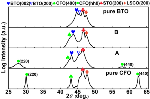
Figure shows the XRD θ − 2θ scan spectra of pure BTO film, pure CFO film and BTO–CFO composite films A, B, all of which were sputtered on (100) SrTiO3 substrates under similar conditions. The pure BTO film shows a tetragonal perovskite structure with {002} and {200} preferred orientations, characteristic of an elastic polydomain microstructure [Citation22–Citation24], while the pure CFO film shows a cubic spinel structure with {440} and {400} preferred orientations [Citation25]. In composite film A, perovskite BTO and spinel CFO coexist as predominant phases with the same preferred orientations as those in the single phase films. On the other hand, film B only shows {001} and {400} preferred orientations in BTO and CFO phases, respectively, most likely due to an enhanced strain effect in the composite film. Compared with those of the pure films, the diffraction peaks of BTO and CFO component phases in the composite films were shifted to lower 2θ angles, indicating the existence of uncompensated misfit stresses in the composite films [Citation26].
Figure 1 XRD θ − 2θ scan spectra of pure BTO film, composite films B and A, and pure CFO film.
Surface morphologies and dispersion of phases
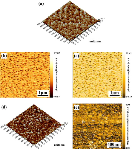
When measured by SPM, the two composite films show distinctively different surface morphologies (figures (a), (d) and AFM images) and dispersion of component phases (figures (b)–(c), (e), PFM and MFM images). In the AFM images, film A shows a uniformly distributed granular surface (figure (a)) while film B shows a ‘mountain-valley’ type of rough surface (figure (d)). Moreover, a self-assembled nanostructure was revealed in film A, as can be seen from its PFM images [Citation27, Citation28]—the brownish red and yellow background areas in both figures (b) and (c) show zero piezoelectric signal, corresponding to the non-piezoelectric CFO phase, while the well-dispersed dark ‘particles’ showing piezoelectric signals are the ferroelectric BTO phase. With an average lateral size of ∼100 nm and a uniform distribution, the BTO phase formed a self-assembled nanostructure in the CFO matrix. In contrast, film B shows a poor dispersion of component phases in its MFM image (figure (e))—the matrix BTO phase shows as a bright yellow area with a zero magnetic force, while the minority CFO phase that exerts a magnetic force to the scanning tip shows as a dark or white strips dispersing in the BTO matrix. The ferroelectric BTO particles are weakly inter-connected, resulting in a poor dispersion of the phases, as can be clearly seen in the MFM image. From the above analysis, it is expected that film A should show better composite properties than film B.
Figure 2 (a) AFM image (5 μm × 5 μm), (b), (c) out-of-plane and in-plane PFM images (5 μm × 5 μm) of composite film A; (d) AFM (2 μm × 2 μm) and (e) MFM (2 μm × 2 μm) images of composite film B.
Dielectric properties
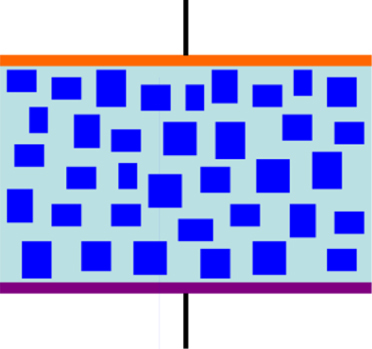
Figure shows the frequency-dependent room temperature dielectric constant and loss tangent of the single phase and composite films. Compared with the pure BTO film which shows a typical bulk-like frequency-dependent dielectric property, film A has not only a larger dielectric constant and a lower dielectric loss but also much reduced frequency dispersion behavior. In fact, when the applied frequency increases from 1 kHz to 2 MHz on film A, its dielectric constant only decreases from 491 to 379 (∼ 20% reduction), and the dielectric loss tangent decreases from 0.12 to 0.04. These are in strong contrast to the ∼ 95% decrease in dielectric constant (from ∼ 380 to 20) and a loss tangent peak (∼ 1.8) around 1 MHz observed in the pure BTO film in the same frequency range. Improvement of the dielectric property in this nanocomposite film can be explained by the widely accepted ‘micro-capacitor’ model. As can be seen from table and the PFM images shown in figures (b) and (c), a large volume fraction of the conductive CFO phase and its heteroepitaxial interaction with the insulating BFO phase allowed a uniform dispersion of the latter at the nanoscale in a conductive matrix, forming many ‘micro-capacitors’ (see figure ). Consequently, the increase of the apparent dielectric constant can be attributed to the decrease of the effective thickness of the dielectric layer and the increase of the effective electrode area. On the other hand, the effect of size may account for the reduced dielectric loss and suppressed frequency dispersion, since micro-capacitors have reduced conduction loss and different relaxation mechanisms to their large counterparts [Citation29].
Figure 3 Dielectric constants and losses of composite films (a) A, and (b) B (compared with that of pure BTO thin film prepared under similar conditions).
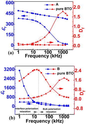
Figure 4 Schematic representation of the ‘micro-capacitors’ model.
On film B which has a low volume ratio of CFO, the dielectric behavior is distinctively different. Film B has an extremely large dielectric constant at low frequency. In fact, its dielectric constant of ∼ 3100 at 1 kHz is an eight-fold improvement against that of the pure BTO film (see figure (b)). However, as the measuring frequency is increased from 1 to 20 kHz, the dielectric constant of film B decreases sharply to a low value of ∼ 240. When the frequency is further increased from 20 kHz to 2 MHz, the dielectric constant slowly declines to ∼ 90 and the loss tangent drops to a low level of ∼ 0.21 (see figure (b)). It is known that space charge polarizations can be induced from boundary mismatches between a conductor and an insulator [Citation30, Citation31]. Such boundary mismatches are abundant in film B where conductive CFO particles are embedded in the BTO insulator matrix [Citation30, Citation31]. In this configuration, the BTO phase is inter-connected and there are far fewer ‘micro-capacitors’ formed. Therefore, the polarization contribution from space charges is dominant. According to the Maxwell–Wagner effect, space charge polarizations contribute to the increase of the apparent dielectric constant and a high dielectric loss at low frequency. As the measuring frequency is increased to the order of ∼ 10 kHz, relaxation of interface polarizations occur and the apparent dielectric constant will drop quickly. In the medium frequency range (∼ 100 kHz to 1 MHz), bulk polarization relaxation becomes the dominant loss mechanism. An interface-ruling dielectric should exhibit a slowly declining dielectric constant and a decreasing loss tangent. Overall, the space charge model explains the frequency-dependent dielectric behavior of film B very well.
The dielectric properties of our FFC can be mainly explained by considering the competing effects between the space charge polarization and ‘micro-capacitors’. When the insulating BTO is well-dispersed in the conductive CFO matrix phase, the ‘micro-capacitors’ effect dominates, inducing an optimal dielectric percolation behavior. On the other hand, when the conductive CFO phase is dispersed in the insulating BFO matrix, the space charge effect takes control, leading to an enhanced low-frequency dielectric constant and increasing dielectric loss.
The effect of preferred orientations on dielectric properties can be very important for single phase films [Citation32] or bulk materials [Citation33–Citation35]. For example, the so-called ‘domain engineering’ took advantage of the large crystalline anisotropies in BTO single crystals or ceramics, resulting in significantly enhanced electromechanical properties [Citation33–Citation35]. However, due to the extra elastic constraint imposed by the co-sputtered phase of CFO (a weak dielectric), as well as a dominant extrinsic contribution from percolative dielectric behavior, contribution from crystalline anisotropy of BTO to the dielectric properties is negligible in our composite films. This is evidenced by finding the largest quasi-static dielectric constant of all films in film B, which contains the least amount of {200} BTO. These in-plane oriented crystallites should exhibit a ten times larger quasi-static dielectric constant than their out-of-plane peers according to the crystalline anisotropy of BTO [Citation36].
Leakage current and ferroelectric properties
Figure (a) shows I–V leakage current curves of pure BTO, pure CFO and A, B nanocomposite films. It is noted that while the pure BTO film is a good insulator up to an applied voltage of 20 V, the pure CFO film is a poor insulator with a leakage current six orders of magnitude larger than the former. Interestingly, although film A has a larger CFO concentration than that of film B, its leakage current is much lower and sustains at modest values (< 1 μA) up to 20 V. On the other hand, the leakage current of film B increases rapidly with the applied voltage and exceeds 1 μA at 5 V. These results describe the quasi-static conduction behavior of the films. In the present case, they cannot be explained by the simple lever rule of composites. Instead, the I–V characteristics are consistent with the measured dielectric properties. While the ‘micro-capacitor’ dominant composite film (film A) shows a modest leakage current, the space-charge dominant composite film (film B) has a much larger conduction loss.
Figure 5 (a) I–V leakage currents of composite films A and B, pure BTO and pure CFO films; polarization hysteresis curves of composite films (b) A and (c) B (@1 kHz). The values of polarizations have been normalized with respect to volume fractions of the BTO phase.
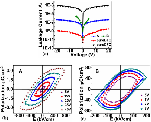
Figures (b) and (c) are the room temperature polarization-electric field (P–E) hysteresis loops of composite films A and B, respectively. The remnant polarization (Pr) and coercive field (Ec) of the two composite films increase with an applied electric field, indicating that a high electric field is required to obtain saturation of polarization. Film B has a low up limit of applied voltage (8 V, ∼ 200 kV cm−1) and leaky P–E curves, which are consistent with its large leakage current. In contrast, the less leaky composite film A shows much better ferroelectric characteristics in its P–E curves. The normalized maximum polarization (Pm), remnant polarization (Pr) and the coercive field under an applied field of 800 kV cm−1 are ∼ 3.4 μC cm−2, 2.3 μC cm−2 and 400 kV cm−1, respectively, while those of the pure BTO film at the same applied field are 21 μC cm−2, 2.7 μC cm−2 and ∼ 200 kV cm−1. The significant reduction of Pm and increase of Ec can be explained by elevated energy barriers for domain wall movement and domain switching in the composite film. This is attributed to the extra elastic clamping imposed by the non-ferroelectric CFO, which is heteroepitaxially grown along the out-of-plane direction with the ferroelectric BTO.
Conclusions
An rf magnetron co-sputtering method, which is capable of in situ tuning of the volume fraction of component phases in a composite film, has been successfully applied in the preparation of self-assembled percolative BTO–CFO nanocomposite films. Highly oriented crystalline phases of {001} perovskite BTO and {100} spinel CFO are confirmed to exist in both the single phase and the composite films by XRD analysis, due to the close lattice matching between the phases and the substrates. Scanning probe microscopy analysis reveals that the composite film with a high sputtering power (100 W) of CFO has a uniform dispersion of the BTO phase in the CFO matrix, forming a self-assembled nanocomposite. Such a nanocomposite shows a dielectric percolation with significantly enhanced dielectric constant and suppressed dielectric loss in a broad frequency range. In contrast, the other film with a low sputtering power (50 W) of CFO shows dispersion of the CFO phase in the weakly inter-connected BTO matrix, corresponding to an enhanced low-frequency dielectric constant and an increased dielectric loss, as well as stronger frequency dependences of the two parameters. The two distinctively different percolation behaviors may be explained by considering the competing effects to dielectric properties between the space charge polarization and ‘micro-capacitors’. The leakage current and ferroelectric characteristics of the films are consistent with their dielectric properties.
Overall, it is demonstrated that the dielectric properties of a FFC film can be engineered in its deposition process via magnetron co-sputtering, by simply adjusting the sputtering power of individual targets. Such an experimental approach is also applicable to other FFC films, for example, those containing a lead-based perovskite and/or another spinel ferrite-like nickel ferrite.
Acknowledgments
The authors thank the NSFC of China for financial support (project grant numbers 51002088 and 91122024) and the Shandong Province Outstanding Young Scientist Research Fund (project grant number BS2010CL029). JO would also like to thank the ‘Qi-Lu Young Scholar Fund’ of Shandong University and the project sponsored by the Scientific Research Foundation (SRF) for the Returned Overseas Chinese Scholars, State Education Ministry (ROCS, SEM).
References
- ZhengH 2004Multiferroic BaTiO3–CoFe2O4 nanostructures Science 303 661 663 661–3 10.1126/science.1094207
- FiebigM 2005Revival of the magnetoelectric effect J. Phys. D: Appl. Phys. 38 R123 R152 R123–52 10.1088/0022-3727/38/8/R01
- VazC A FHoffmanJAhnC HRameshR 2010Magnetoelectric coupling effects in multiferroic complex oxide composite structures Adv. Mater. 22 2900 2918 2900–18 10.1002/adma.200904326
- NanC W 1993Physics of inhomogeneous inorganic materials Prog. Mater. Sci. 37 1 116 1–116 10.1016/0079-6425(93)90004-5
- PecharromanCMoyaJ S 2000Experimental evidence of a giant capacitance in insulator–conductor composites at the percolation threshold Adv. Mater. 12 294 297 294–7 10.1002/(SICI)1521-4095(200002)12:4%3C294::AID-ADMA294%3E3.0.CO;2-D
- BergmanD JImryY 1977Critical behavior of the complex dielectric constant near the percolation threshold of a heterogeneous material Phys. Rev. Lett. 39 1222 1225 1222–5 10.1103/PhysRevLett.39.1222
- HyugaHHayashiYSekinoTNiiharaK 1997Fabrication process and electrical properties of BaTiO3/Ni nanocomposites Nano-Struct. Mater. 9 547 550 547–50 10.1016/S0965-9773(97)00121-9
- ZhengHStraubFZhanQYangP LHsiehW KZavalicheFChuY HDahmenURameshR 2006Self-assembled growth of BiFeO3–CoFe2O4 nanostructures Adv. Mater. 18 2747 2752 2747–52 10.1002/adma.200601215
- DengCZhangYMaJLinYNanC W 2008Magnetoelectric effect in multiferroic heteroepitaxial BaTiO3–NiFe2O4 composite thin films Acta Mater. 56 405 412 405–12 10.1016/j.actamat.2007.10.004
- SterbinskyG E 2010 PhD Dissertation Northeastern University, Evanston, IL
- ZhangJ XDaiJ YLuWChanH L W 2009Room temperature magnetic exchange coupling in multiferroic BaTiO3/CoFe2O4 magnetoelectric superlattice J. Mater. Sci. 44 5143 5148 5143–8 10.1007/s10853-009-3512-x
- LiuMObiOCaiZLouJYangGZiemerK SSunN X 2010Electrical tuning of magnetism in Fe3O4/PZN-PT multiferroic heterostructures derived by reactive magnetron sputtering J. Appl. Phys. 107 073916 10.1063/1.3354104
- DelgadoEOstosCMartínez-SarriónL M LMestresLLedermanDPrietoP 2009 Growth and characterization of BLZT–CFO composite thin films Mater. Chem. Phys. 113 702 706 702–6 10.1016/j.matchemphys.2008.07.131
- FinaIDixNLaukhinVFabregaLSanchezFFontcubertaJ 2009 Dielectric properties of BaTiO3–CoFe2O4 nanocomposite thin films J. Magn. Magn. Mater. 321 1795 1798 1795–8 10.1016/j.jmmm.2009.02.012
- ZhangLZhaiJMoWYaoX 2010Dielectrical and magnetic properties of CoFe2O4–BaTiO3 composite films prepared by a combined method of sol-gel and electrophoretic deposition J. Am. Ceram. Soc. 93 3267 3271 3267–71 10.1111/j.1551-2916.2010.03823.x
- ZhouDJianGZhengYGongSShiF 2011 Electrophoretic deposition of BaTiO3/CoFe2O4 multiferroic composite films Appl. Surf. Sci. 257 7621 7626 7621–6 10.1016/j.apsusc.2011.03.141
- ZhangLZhaiJMoWYaoX 2009Electrical and dielectric behaviors of composite CoFe2O4–BaTiO3 thick films Mater. Chem. Phys. 118 208 212 208–12 10.1016/j.matchemphys.2009.07.031
- RoySMajumderS B 2011 Percolative dielectric behavior of wet chemical synthesized lead lanthanum titanate–cobalt iron oxide composite thin films Phys. Lett.A 375 1538 1542 1538–42 10.1016/j.physleta.2011.02.046
- EomC BSunJ ZYamamotoKMarshallA FLutherK ELadermanS SGeballeT H 1989 In situ grown YBa2Cu3O7−d thin films from single-target magnetron sputtering Appl. Phys. Lett. 55 595 597 595–7 10.1063/1.102436
- CaoL ZFuW YWangS FWangQSunZ HYangHChengB LWangHZhouY L 2007 Effects of film thickness and preferred orientation on the dielectric properties of (Bi1.5Zn0.5)(Zn0.5Nb1.5)O7 films J. Phys. D: Appl. Phys. 40 2906 2910 2906–10 10.1088/0022-3727/40/9/036
- ArtemevASlutskerJRoytburdA L 2005Phase field modeling of self-assembling nanostructures in constrained films Acta Mater. 53 3425 3432 3425–32 10.1016/j.actamat.2005.04.016
- ZhangWOuyangJRoytburdA L 2012 Effect of thickness-mediated misfit strain on the heterophase polydomain structure of epitaxial BiFeO3 films Scr. Mater. 66 499 502 499–502 10.1016/j.scriptamat.2011.12.030
- OuyangJSluskerJLevinIKimD MEomC BRameshRRoytburdA L 2007Engineering of self-assembled domain architectures with ultra-high piezoelectric response in epitaxial ferroelectric films Adv. Funct. Mater. 17 2094 2100 2094–100 10.1002/adfm.200600823
- RoytburdA L 1998Thermodynamics of polydomain heterostructures J. Appl. Phys. 83 228 245 228–45 10.1063/1.366677
- LiuYRuanXZhuBChenSLuZShiJXiongR 2011 CoFe2O4/BaTiO3 composites via spark plasma sintering with enhanced magnetoelectric coupling and excellent anisotropy J. Am. Ceram. Soc. 94 1695 1697 1695–7 10.1111/j.1551-2916.2011.04582.x
- ZhangWYuanMWangXPanWWangC MOuyangJ 2012 Design and preparation of stress-free epitaxial BaTiO3 polydomain films by RF magnetron sputtering Sci. Technol. Adv. Mater. 13 035006 10.1088/1468-6996/13/3/035006
- FrankeKBesoldJHaesslerWSeegebarthC 1994Modification and detection of domains on ferroelectric PZT films by scanning force microscopy Surf. Sci. Lett. 302 283 288 283–8 10.1016/0039-6028(94)91089-8
- GruvermanAAucielloOTokumotoH 1996Scanning force microscopy for the study of domain structure in ferroelectric thin films J. Vac. Sci. Technol. B 14 602 605 602–5 10.1116/1.589143
- WuLChureM CWuK KChangW CYangM JLiuW KWuM J 2009Dielectric properties of barium titanate ceramics with different materials powder size Ceram. Int. 35 957 960 957–60 10.1016/j.ceramint.2008.04.030
- YuZAngC 2002Maxwell–Wagner polarization in ceramic composites BaTiO3–(Ni0.3Zn0.7)Fe2.1O4 J. Appl. Phys. 91 794 797 794–7 10.1063/1.1421033
- ChenZHuangJChenQSongCHanGWengWDuP 2007A percolative ferroelectric–metal composite with hybrid dielectric dependence Scr. Mater. 57 921 924 921–4 10.1016/j.scriptamat.2007.07.020
- YangLPonchelFWangGRémiensDLégierJ FChateignerDDongX 2010 Microwave properties of epitaxial (111)-oriented Ba0.6Sr0.4TiO3 thin films on Al2O3 (0001) up to 40 GHz Appl. Phys. Lett. 97 162909 10.1063/1.3478015
- WadaSYakoKKakemotoHTsurumiTKiguchiT 2005Enhanced piezoelectric properties of barium titanate single crystals with different engineered-domain sizes J. Appl. Phys. 98 014109 10.1063/1.1957130
- ParkS EWadaSCrossL EShroutT R 1999Crystallographically engineered BaTiO3 single crystals for high-performance piezoelectrics J. Appl. Phys. 86 2746 2750 2746–50 10.1063/1.371120
- WadaSTakedaKTsurumiTKimuraT 2007 Preparation of [110] grain oriented barium titanate ceramic by templated grain growth method and their piezoelectric properties Japan. J. Appl. Phys. 46 7039 7043 7039–43 10.1143/JJAP.46.7039
- ZgonikMBernasconiPDuelliMSchlesserRGunterPGarrettM HRytzDZhuYWuX 1994 Dielectric, elastic, piezoelectric, electro-optic, and elasto-optic tensors of BaTiO3 crystals Phys. Rev. B 50 5941 5949 5941–9 10.1103/PhysRevB.50.5941