
Abstract
Photonic crystals consist of artificial periodic structures of dielectrics, which have attracted much attention because of their wide range of potential applications in the field of optics. We may also fabricate artificial amorphous or quasicrystalline structures of dielectrics, i.e. photonic amorphous materials or photonic quasicrystals. So far, both theoretical and experimental studies have been conducted to reveal the characteristic features of their optical properties, as compared with those of conventional photonic crystals. In this article, we review these studies and discuss various aspects of photonic amorphous materials and photonic quasicrystals, including photonic band gap formation, light propagation properties, and characteristic photonic states.
Introduction
In 1987, Yablonovitch [Citation1] and John [Citation2] pointed out that a frequency range in which light propagation is forbidden in all directions, i.e. a three-dimensional (3D) photonic band gap (PBG) can be realized in artificial periodic dielectric structures, namely, photonic crystals. They also discussed novel types of light phenomena possibly brought about by the 3D-PBG. Most importantly, the 3D-PBG enables 3D light confinement within a wavelength-sized volume without a corresponding substantial loss, which is difficult to achieve in other media. Because such strong light confinement should enhance various light–matter interactions and realize very efficient nanophotonic devices, photonic crystals have attracted broad interest and have since been studied extensively [Citation3]. It was later recognized that not only PBGs but also photonic bands (PB), in which light propagation modes exist, have interesting properties. They have also been important research subjects up to the present day. On the other hand, it has been shown that the realization of a 3D-PBG is much more difficult in practice than initially appeared. Meanwhile, it has been found that more easily realizable two-dimensional (2D) PBGs by 2D photonic crystals also enable rather strong light confinement with a proper structural design. Because of these findings, 2D photonic crystals have recently been studied more intensively than 3D photonic crystals.
In 1984, a material with a peculiar type of order in its atomic arrangement, which was essentially different from the periodic order in conventional crystals, was discovered [Citation4], and was subsequently named a quasicrystal. Following thirty years of research on quasicrystals, this discovery has been recognized as a truly epoch-making event in materials science. For this reason, Shechtman, the discoverer of the quasicrystal, won the Nobel Prize in chemistry in 2011.
What happens if we transfer quasicrystalline structures to photonic crystals? What about amorphous structures? So far, both theoretical and experimental studies of these photonic quasicrystals and photonic amorphous materials have been conducted to reveal the characteristic features of their optical properties, as compared with those of conventional photonic crystals. The purpose of the present article is to review these studies and discuss various aspects of photonic quasicrystals and photonic amorphous materials. Here, we mainly focus on whether photonic devices based on them can be more efficient than those of standard photonic crystals and whether they can exhibit novel properties that conventional photonic crystals do not possess. This article is organized as follows. First, in the following section, section 2, some important aspects of the physics and engineering of photonic crystals are summarized. Sections 3 and 4 are devoted to photonic amorphous materials and photonic crystals, respectively. Finally, in section 5, a summary is given, and future prospects of the non-periodic photonic materials are discussed.
Photonic crystals
Photonic band structure
In this subsection, the concept of photonic band structure, which plays an essential role in understanding the physical phenomena of light in photonic crystals, is briefly reviewed. Detailed explanations are already given in many textbooks [Citation5–Citation7].
Because light is an electromagnetic wave, its behaviour is governed by Maxwell’s equations(1)
where
is the electric field,
is the magnetic field,
is the electric displacement field,
is the magnetic induction field,
is the free charge density, and
is the current density. Here, we restrict our discussion to the photonic crystals of dielectrics, although there also exist photonic crystals made of metals. Because metals are not included,
. Magnetic materials are not included either, and, therefore,
(
: the vacuum permeability). Furthermore, there are no free charges, i.e.
. We assume that the dielectrics satisfy
(
: the relative permittivity,
: the vacuum permittivity), where
is a function of the position r, i.e.
In most cases, photonic crystals consist of dielectrics with
and air with
. With these conditions, Maxwell’s equations of equation (Equation1
(1) ) transform to:
(2)
Here, let us examine the stationary solutions given by(3)
Inserting equation (Equation3(3) ) into (Equation2
(2) ) gives
(4)
We cancel from the third and fourth equations in equation (Equation4
(4) ) to obtain
(5) where
is the vacuum speed of light. Equation (Equation5
(5) ) has the form of an eigenvalue problem with the linear operator
. This is similar to the fact that the electronic wavefunctions
of the eigenstates in a potential
are given by the equation
(6) where
is the Hamilton operator,
is the electron mass, and
is the electron eigenenergy. By solving equation (Equation5
(5) ) for a given structure
under the condition of the second equation in equation (Equation4
(4) ), we obtain the fields
and the corresponding frequencies
. Then, by inserting the obtained
into the fourth equation in equation (Equation4
(4) ), we obtain
. Here, the first equation in equation (Equation4
(4) ) is automatically satisfied.
When, in equation (Equation5(5) ),
has a periodicity, and therefore the operator
is periodic, Bloch’s theorem holds, similarly to the case of the electronic system in equation (Equation6
(6) ) with a periodic
. Then, the eigenstates can be labelled by a Bloch wave vector
and a band index
where
lies in the first Brillouin zone (Z). The eigenfrequency
is a continuous function of
in each band, having the form
(k ∊ Z,
). This is called the photonic band structure.
In 2D photonic crystals where has a 2D periodicity in the
plane and is constant along the
direction, the electromagnetic fields of
and
, and those of
and
are decoupled, where
denotes the positional vector in the
plane. The former is called the transverse electric (TE) mode and the latter is called the transverse magnetic (TM) mode. They independently give respective photonic band structures.
The photonic density of states (DOS) is given by:
(7)
similar to the electronic DOS in electronic systems, where
is 2 in 2D systems and 3 in 3D systems.
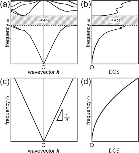
In figure (a), the photonic band structure of a photonic crystal is illustrated schematically. The corresponding photonic DOS is illustrated in figure (b). For comparison, the relation and the photonic DOS in a homogeneous medium with refractive index
are shown in figures (c) and (d), respectively. In photonic crystals, the simple
relation in figure (c) is largely modified to a complicated relation such as in figure (a). In particular, a frequency range in which no photonic states exist can be formed if we design the structure properly. This frequency range is called the photonic band gap (PBG). PBGs in 3D systems, i.e. 3D-PBGs, are called, in particular, complete PBGs. In general, all the information on the light propagation properties of a given photonic crystal is included in its photonic band structure. By looking at the photonic band structure, we can tell whether light with a given frequency propagates or not, and, if it propagates, we can tell in what direction and at what speed it propagates. The aim of the engineering of photonic crystals is simply to design a structure of a photonic crystal that produces a desired photonic band structure to realize a desired light propagation behaviour.
Figure 1 Illustrations of (a) a photonic band structure and (b) the corresponding photonic DOS for a photonic crystal, and (c) a relation and (d) the corresponding photonic DOS for a homogeneous medium with refractive index
.
Functions and applications of photonic crystals
Typical examples of the applications of photonic crystals are summarized in table [Citation5–Citation7], where they are classified into two groups: applications utilizing the PBG and those utilizing the PB. If a photonic crystal forms a complete 3D-PBG, light with a frequency that is within the complete PBG cannot propagate in any 3D direction in the photonic crystal. This behaviour of light could never be realized in homogeneous media with a simple relation such as in figure (c). If such a photonic crystal is externally irradiated with light with a frequency that is within the complete PBG, then the incident light should be totally reflected, irrespective of the incident angle. Therefore, photonic crystals with a complete PBG can act as a mirror that selectively reflects light of a particular frequency (or wavelength) range. At the same time, they can also act as a filter that transmits light of a particular frequency (or wavelength) range outside the PBG.
Table 1 Typical examples of the applications of photonic crystals.
If we introduce a point defect to a photonic crystal with a PBG, a defect level is created in the PBG and a photonic state localized at the defect position is formed. This indicates that we can confine light with a specific frequency three-dimensionally to the introduced defect position. Such a defect can act as an optical resonator with an extremely small size. By combining such a defect with laser media, a minuscule laser (a point-defect laser) can be realized. If we introduce a line defect, light can be confined two-dimensionally in the plane perpendicular to the line, and light can propagate only along the line. Such a line defect can act as an optical waveguide. It appears that a complete 3D-PBG is indispensable for 3D light confinement by a point defect and 2D light confinement by a line defect. However, it has been shown that 2D slab-type photonic crystals can also confine light rather strongly if we design the structure properly [Citation3, Citation5–Citation7]. Here, the 2D-PBG confines light in the plane, and the refractive-index difference between the photonic crystal slab and air confines light in the
direction. Combining optical resonators and optical waveguides is expected to lead to various types of light-controlling devices, such as an optical multiplexer/demultiplexer and optical switches with a minuscule size. Much effort has been devoted to realizing these devices, and it is believed that an optical integrated circuit consisting of such minuscule devices will be realized in the future.
Applications utilizing PBs are based on the fact that the direction and speed of light propagation in photonic crystals are governed by the group velocity given by(8)
Here, we attempt to realize a desired light propagation behaviour by designing the structure to obtain a desired . While in homogeneous media
is always parallel to
of the plane wave, and
is constant
irrespective of
or
, in photonic crystals
can be altered fairly freely by the design of the structure. For example, an optical time delay device can be realized if we obtain a small value of
. Using the group velocity dispersion, i.e. the k-dependence of
, we can perform the dispersion compensation of optical pulse signals. We generally obtain standing waves with
at the band edges in photonic crystals. Using such optical states, distributed feedback lasers can be realized.
An anomalous refraction phenomenon can be realized by controlling . In general, the angle-dependence of refraction at the interface between a homogeneous medium and another homogeneous medium obeys Snell’s law. This law should be modified when one of the two media is replaced with a photonic crystal, because the law is derived on the assumption that the
relations of both media are isotropic and linear. An anomalous refraction should take place at the interface between homogeneous media such as air and a photonic crystal. Such anomalous refractions are generally called superprism effects. In particular, by properly designing
, a refraction that obeys Snell’s law with a negative value of
for the photonic crystal can occur. This phenomenon is called negative refraction [Citation8], by which we can realize a lens that enables a peculiar imaging.
Formation mechanisms for the photonic band gap
Of the functions and applications of photonic crystals described in the preceding subsection, those related to PBGs were the first to attract attention, and only later those utilizing PBs were noticed. However, PBG-related applications are still regarded as the most important objective, particularly the realization of small-sized light-controlling devices and optical integrated circuits using the light confinement effect. For this purpose, we have to first prepare a photonic crystal with a PBG. Here, a wider PBG is favourable to yield a stronger light confinement effect. On the other hand, a smaller critical dielectric contrast, , to open the PBG is favourable from the viewpoint of material selection. In this subsection, we discuss the formation mechanism for PBGs in photonic crystals.
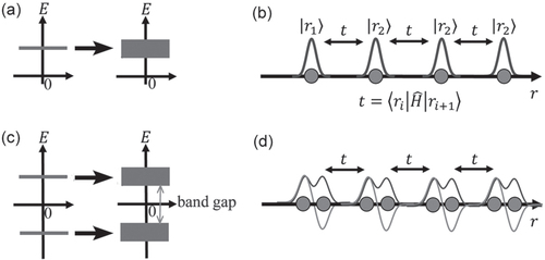
Owing to the similarity between the basic equations describing the electronic states in solid crystals and those describing the photonic states in photonic crystals, the formation mechanisms for the electronic band gap are also essentially applicable to the formation of the PBG in photonic crystals. There are two typical models to explain the origin of the electronic band gaps in solids: the ‘nearly free electron model’ and the ‘tight-binding model’, which are illustrated schematically in figures and , respectively.
Figure 2 Illustrations of the nearly free electron model. (a) The parabolic relation shown in the left-hand side for a free electron is modified to the
relation in the right-hand side as a result of the addition of a periodic potential. (b) The potential
and the electronic states at A and B in the right-hand side in (a).
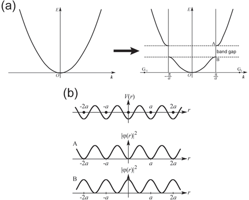
Figure 3 Illustrations of the tight-binding model. (a) The energy level for the isolated localized states extends and forms a band by the addition of the couplings (t) between adjacent bases. (b) The localized bases and the couplings (t) between adjacent bases. (c) and (d) correspond to (a) and (b), respectively, for the case in which there are two localized states with different energies.
In the nearly free electron model, we begin with the free electron model, in which the plane-wave bases become the eigenstates as they are, and we add a weak periodic potential as a perturbation. Then, energy gaps are created along the Bragg scattering planes (i.e. the bisecting planes of the line segments linking between the origin and each reciprocal lattice point in the reciprocal space) as a result of interference effects from Bragg scattering. In a one-dimensional (1D) model, the parabolic relation shown in the left-hand side of figure (a) for a free electron is modified to the
relation in the right-hand side as a result of the addition of a periodic potential with period a. Here, an energy gap is created at
by the interference of the waves
and
, which travel in opposite directions. They form standing waves that give the eigenstates at points A and B in the
relation in the right-hand side of figure (a). Here, the former has the amplitude at high
regions while the latter has the amplitude at low
regions, as shown in figure (b). This results in a potential energy difference for the electron, leading to the formation of the electronic energy gap.
This type of mechanism should also work for PBG formation in photonic crystals, hereafter called the mechanism of the Bragg-scattering origin. The PBG formations in most photonic crystals are believed to be due to this mechanism. Dielectric and air regions in the field in photonic crystals correspond to the low and high potential regions, respectively, of the electrons in crystalline solids. Therefore, we often observe the
field to be concentrated in the dielectric region at the top of the lower band and in the air region at the bottom of the upper band in photonic crystals with a PBG, as in the case of the electronic system shown in figure . For this reason, we often call the lower band the dielectric band and the higher band the air band [Citation5–Citation7].
In 3D photonic crystals, the structures in which the dielectric region forms a connected and percolating network are known to favour gap formation [Citation9–Citation11]. Now, let us consider a hypothetical photonic state in which the field is completely concentrated in the dielectric region. Then, the first equation in equation (Equation4
(4) ) in section 2.1 requires that the vector field of
form a current without source nor sink within the dielectric region. Here, in order for the
field to be confined in the dielectric region, it must be a connected network to accommodate the continuous field lines [Citation5], as schematically shown in figure (a). The eigenstate just above such a state in terms of eigenfrequency should concentrate the
field in the air region to maintain orthogonality with the state, creating a jump in eigenfrequency to form a PBG. Then, if we segment the dielectric network, there is no longer a continuous pathway to accommodate the whole
field lines in the dielectric regions; they are forced to penetrate the air regions, as shown in figure (b). This should raise the eigenfrequency at the lower-band top, leading to a closing of the gap. In fact, the extreme fragility of the band gap against segmentation of the dielectric network in a 3D photonic crystal has been demonstrated by numerical calculations [Citation19].
Figure 4 (a) Illustrations of the electric vector field concentrated in the dielectric region. (b) Illustrations of the electric vector field partially leaking into the air region as a result of segmentation of the dielectric network.
Apart from the similarity between the basic equations describing the electronic states in solid crystals and photonic states in photonic crystals, there are also significant differences between them. A major difference lies in the nature of the electronic wavefunction and that of the electromagnetic fields: the former is a scalar field while the latter are vector fields. The advantage of the dielectric network structure in the formation of a 3D-PBG originates with this very point, which is a characteristic feature in the PBG formation and not seen in electronic band gap formation.
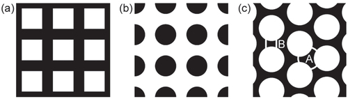
In 2D systems, the structures favourable for TE-mode PBG formation and those for TM-mode PBG formation are different [Citation5]. This is caused by the difference in the nature of the electric field in the 2D plane: it is a vector field in the TE mode and a scalar field in the TM mode. In the TE mode, dielectric network structures such as the structure shown in figure (a) are favourable, similar to the case of 3D photonic crystals. In contrast, in the TM mode, arrangements of isolated dielectric units such as the structure in figure (b) are favourable. As long as the square lattice structures in figures (a) and (b) are concerned, only the TE mode PBG is formed in figure (a) while only the TM mode PBG is formed in figure (b), at a Si–air dielectric contrast, that is, . To realize PBGs in both of the two modes, we need to adopt a structure with the characteristics of both structures, as shown in figure (c). Here, we have a triangular lattice of air columns. In this structure, the areas at the centres of the three columns, such as region A, resemble isolated dielectric regions, which are connected to each other through the areas between two columns, such as region B. This structure has been shown to form both TE and TM PBGs at
, and, in addition, they have a common frequency range. We hereafter call such a gap with a frequency range common to the two modes the ‘TE-TM common PBG’.
Figure 5 Examples of a 2D structure favourable for (a) TE-PBG formation, (b) TM-PBG formation, and (c) TE-TM common PBG formation. Black and white correspond to the dielectric and air regions, respectively. For an explanation of the A and B regions, see text.
The tight-binding model shown schematically in figure is an extreme opposite to the nearly free electron model. This model begins with localized bases at individual atoms (figure (b)). When the atoms are arranged with sufficient separation, the couplings (t) between adjacent bases should be zero, and these localized bases become the eigenstates as they are. As the interatomic distance decreases, the couplings between the adjacent bases grow, leading to band formation (figure (a)). If we first assume two localized states with different energies, two bands are created (figure (c)). If the energy difference between the two localized states is sufficiently large, and/or if the widths of the bands formed by the couplings are sufficiently small, then a band gap should be left. The two localized states that we first assumed may be two different states in an atom or may be the bonding and anti-bonding states formed by two adjacent atoms (figure (d)). In any case, in this mechanism the band gap formation originates in two localized states arising from the local structure.
In photonic crystals, the photonic states of the Mie resonances of the isolated dielectric spheres in 3D or the isolated dielectric columns in 2D possibly play the same role as the localized bases in the electronic case [Citation7]. We hereafter call this mechanism for PBG formation the mechanism of the Mie-resonance origin. In contrast to the mechanism of the Bragg-scattering origin, this mechanism does not necessarily require long-ranged structural order such as periodicity and quasiperiodicity.
Shi et al [Citation12] have investigated PBG formation by finite-difference time-domain (FDTD) calculations in a series of 2D photonic crystals consisting of a square lattice of dielectric columns with different values of the parameters (the ratio of the column radius to the lattice constant) and
(the dielectric contrast). They have shown that PBG formation can be interpreted as due to the mechanism of the Bragg-scattering origin in a weak scattering regime with small
and
, and as due to the mechanism of the Mie-resonance origin in a strong scattering regime with large
and
.
Photonic amorphous materials
Even for amorphous structures possessing without periodicity, equations (Equation1
(1) )–(Equation5
(5) ) in section 2.1 hold as they are. However, Bloch’s theorem does not hold and the Bloch wave vector
becomes meaningless. Therefore, the set of the functions
i.e. the photonic band structure, cannot be defined. However, the photonic DOS
can be defined by the first equation in equation (Equation7
(7) ), and if we have a frequency range
free from the states, then we can call it a PBG. If a photonic amorphous material possesses a PBG, then it can be used for applications that utilize the PBGs of photonic crystals listed in table . On the other hand, those utilizing PBs in table are essentially not applicable to the photonic amorphous materials because the eigenstates are not characterized by
vectors. Light propagation behaviours in PBs in photonic amorphous materials should be very different from those in photonic crystals. In this section, we review PBG formations and the light propagation properties of photonic amorphous materials.
Photonic band gap formation
In 2001, Jin et al [Citation13] reported the formation of a TM-PBG in a 2D photonic amorphous structure of an arrangement of dielectric columns. This structure was constructed by introducing disorder into a periodic square lattice structure. Subsequently, in 2003, Miyazaki et al [Citation14] showed the formation of a TM-PBG in a 2D photonic amorphous structure constructed by arranging randomly dielectric columns under the conditions of a given minimum inter-column distance and a given number density of the column. When the imposed number density is low, void regions without columns are generated, and no noticeable TM-PBG is formed. On the other hand, when the number density is sufficiently high, the structure becomes homogeneous without the formation of voids, forming a TM-PBG. Since then, TM-PBG formations have been reported for similar structures of the arrangement of dielectric columns [Citation15]. It has been shown that in all these cases the necessary conditions to form a TM-PBG are as follows: (i) columns should not be too close to each other and (ii) the structure should be homogeneous without voids. Compared with the hexagonal photonic crystal of dielectric columns, which is the 2D photonic crystal yielding the largest TM-PBG, the sizes of the TM-PBGs of photonic amorphous materials are generally smaller if we adopt the same volume fraction of the dielectric part and the same dielectric contrast.
As described in the last part of section 2.3, Shi et al [Citation12] have shown that PBG formation in a 2D photonic crystal of dielectric columns can be interpreted as being due to the mechanism of the Bragg-scattering origin in a weak scattering regime, and as being due to the mechanism of the Mie resonance origin in a strong scattering regime. PBG formation in photonic amorphous materials should never be caused by the Bragg-scattering origin. In fact, they have been reasonably explained as being caused by the Mie-scattering origin [Citation15]. Condition (i) described in the preceding paragraph for TM-PBG formation is necessary for the Mie resonant states, which is the origin of the gap formation, to not be significantly disturbed. Condition (ii) is necessary because the presence of regions with low density should generate localized states around them. In addition to TM-PBG formation, the formation of a TE-TM common PBG has been reported for a photonic amorphous structure with a geometry similar to that shown in figure (c) [Citation16].
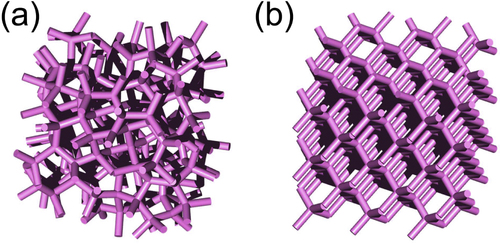
Recently, we have discovered an amorphous structure that forms a complete 3D-PBG [Citation17–Citation19]. The amorphous structure consists of a random network of dielectric rods with a diamond-like local tetrahedral configuration and is therefore named a ‘photonic amorphous diamond’ (PAD) (figure (a)). More specifically, the PAD structure is based on the concept of a ‘continuous random network’ (CRN) that was originally developed to describe the atomic arrangement of amorphous Si or Ge [Citation20]. For comparison, a photonic crystalline diamond (PCD) structure, which is constructed by connecting tetrahedral bonds in the crystalline diamond structure with dielectric rods, is shown in figure (b). This PCD structure is known to be the best 3D-PBG structure exhibiting the largest 3D-PBG of all the photonic crystals studied thus far [Citation9, Citation10]. The PAD and PCD can be regarded as photonic versions of amorphous and crystalline Si, respectively, in electronic systems.
Figure 6 (a) PAD and (b) PCD structures that form a complete PBG [Citation17–Citation19].
We have calculated the frequency distributions of the photonic eigenstates in PAD and PCD using an FDTD spectral method originally developed by Chan et al [Citation21]. In this method, we begin with a random electromagnetic field and calculate its time evolution. The time evolutions at each position are then Fourier transformed into the frequency-domain in order to obtain the frequency distributions of the photonic eigenstates. Here, we used the CRN structure of Barkema and Mousseau [Citation22] for the design of PAD, which consists of a periodically arranged cubic supercell of size (
: rod length). For PCD, we used a crystalline diamond structure with a fictitious supercell
, where
denotes the lattice constant of the crystalline diamond. Using the fictitious supercell structure for PCD enables us to compare the results obtained under exactly the same conditions for PAD and PCD. The rod radius was
, resulting in an air-volume fraction of 78%. The dielectric contrast was
.
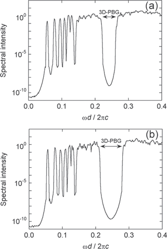
Figures (a) and (b) show the calculation results for PAD and PCD, respectively. In the low frequency region below approximately , both of the spectra have well-isolated peaks. This feature is an artifact arising from the periodic boundary conditions applied to the supercell [Citation17–Citation19]. The formations of a PBG are clearly seen at frequencies in a region around
for both structures. The gap depth in PAD is nearly the same as that in PCD; the spectral intensity at the midgap is lower than that in the passbands by a factor of
, which is the limit of resolution in the present calculations. This fact indicates that the gap in PAD is as clean as that in PCD, with no trace of localized-state formations in the gap. The gap width to the midgap frequency ratio (
) is 18% for PAD and 27% for PCD. Here, the PBG position and width for PCD agree well with those calculated previously [Citation21], indicating the validity of the present calculations. The gap width of PAD is smaller than that of PCD, but still much larger than those of PBG-forming 3D photonic crystals other than PCD and diamond-related photonic crystals. PBG formation in PAD has been verified experimentally through microwave transmission measurements [Citation18, Citation19].
Figure 7 Spectral intensities calculated for the (a) PAD and (b) PCD. They are roughly normalized to the values at the band edges.
The midgap frequencies for PAD and PCD almost coincide with each other, as shown in figures (a) and (b). This fact suggests that the mechanisms for PBG formation in both have the same origin. Because PAD exhibits no Bragg scattering, PBG formation in PAD should never be of the Bragg-scattering origin. This indicates that the mechanism of the Bragg-scattering origin should never be dominant for PBG formation in PCD, although it may work partially. On the other hand, because these are dielectric network structures, the mechanism of the Mie-scattering origin, which is based on isolated scatterers, is not plausible, either. To investigate the PBG formation mechanism, we have examined the field patterns of the photonic eigenstates at the top of the lower band and at the bottom of the higher band [Citation18, Citation19]. Then, we found that the electric fields tend to be concentrated in the dielectric regions at the top of the lower-band, and that they are excluded from the dielectric regions at the bottom of the higher-band for both PAD and PCD. Therefore, the picture of dielectric and air bands, as described in section 2.3, can be applied to PBG formations in these structures. This picture originally comes from the nearly free electron model, and therefore lattice periodicity is assumed in this case. The above results indicate that, in some cases, this picture holds even for amorphous systems. As discussed in section 2.3, network structures should be favourable in this picture because they can feasibly accommodate the continuous field lines. There should be a reason for the fourfold connections to be advantageous in realizing dielectric and air bands, but this is not clear at present.
The structure of PAD has a well-defined local order with a tetrahedral configuration. Then, we can introduce defects by disrupting such an order in PAD. We have shown that point defects introduced by removing a rod create localized photonic states at the defect positions [Citation17, Citation23]. We have calculated the mode volumes (V) and Q-factors for the defect modes, and have compared them with those of point defects in PCD. The defect modes in PAD have exhibited V and Q values comparable to those in PCD, leading to the conclusion that strong light confinement can also be realized with PAD. This is consistent with the fact that the PBG of PAD is as clean as that of PCD, with no trace of localized-state formations in the gap. This is shown in figures (a) and (b). If the PBG in PAD is contaminated with localized states, then the light confined at the introduced defect should leak via such localized states.
In both 2D and 3D systems, if a photonic amorphous material forms a PBG, then it should be isotropic, because the structure is isotropic. This is one of the characteristic features of photonic amorphous materials: the PBGs of photonic crystals invariably display some degree of anisotropy. The isotropic PBG is possibly advantageous in various applications. For example, with regard to the wavelength-selective mirror/filter in table , the selected wavelength range does not change with the orientation of the incident light. If we develop waveguides by introducing line defects, then we may choose their directions freely, as demonstrated in 2D photonic amorphous materials [Citation14, Citation24].
Light propagation properties
Light propagation in random media has been a long-standing subject in optics [Citation25, Citation26]. Here, the term ‘random media’ refers to systems in which light scatterers are distributed randomly. These structures can be regarded as a type of photonic amorphous material. In random media, light undergoes multiple scattering. Then, light propagates diffusively provided the scattering is not very strong. As the scattering intensifies, i.e. the scattering mean free path reduces, light interference intensifies, leading to a halt of diffusive light propagation. This phenomenon is known as the Anderson localization of light [Citation25, Citation27–Citation35]. The criterion for the emergence of Anderson localization is given by
(the Ioffe–Regel (IR) condition [Citation36]), where
denotes the wavelength of light. Research into Anderson localization of light began in the 1980s when Anderson localization in electronic systems in solids was theoretically extended to the photonic system [Citation27]. In the 1990s, Anderson localization of light was demonstrated experimentally [Citation31]. It is thought that the photonic system is more advantageous for elucidating the physical mechanism of Anderson localization than the electronic system. This is because in the latter case electron–electron interaction is expected to complicate the localization phenomena, while in the former case there is no such interaction. This is one of the motivations for studies of Anderson localization of light. This field of research has developed applications such as random lasers, which utilize a lasing action originating in localized photonic states.
In PAD, we have experimentally observed diffusive propagation of electromagnetic waves, and have shown numerically the formation of localized photonic states [Citation18, Citation19]. The results are summarized schematically in figure . As described in the preceding subsection, we have dielectric and air bands, and a PBG between them. Microwave transmission experiments have shown that wave propagation is diffusive in these bands. Here, the scattering mean free path decreases significantly, as the frequency approaches the band edge. At the band edges, the quantity
reaches a value of 3, which is only slightly larger than the threshold value of unity in the IR condition. The quantity
has been evaluated previously for strongly scattering systems close to the Anderson transition in random media comprising GaAs powders (
) [Citation31], macroporous GaP networks (2.4 and 3.2) [Citation33, Citation37], Ge powders (3) [Citation34], and TiO2 powders (2.5 and 5.6) [Citation32, Citation38]. The value
evaluated for our PAD is comparable to these values. By using these strong scattering systems, including PAD, we should be able to realize a very thin light diffuser that can completely eliminate the memory of light polarization and wavevector orientation with a thickness comparable to the wavelength of light.
Figure 8 Schematic illustration of the photonic bands and light propagation behavior in PAD.
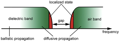
In PAD, the localized states were identified at the band edges through numerical calculations, as shown in figure . This result is consistent with the fact that the mean free path lengths experimentally evaluated at the band edges nearly satisfy the IR condition. The formation of localized photonic states near the band edges in our PAD is analogous to the formation of localized electronic states in amorphous semiconductors.
Photonic quasicrystals
The structure of a quasicrystal is defined as follows [Citation39]. A structure is a quasicrystal if and only if its diffraction intensity function
9 satisfies the following two conditions: (i) it consists of a set of
functions and (ii) it has a rotational symmetry other than those allowed for crystals, i.e. 1-, 2-, 3-, 4-, and 6-fold symmetries. Here,
is the volume of the system and
is the scattering vector. Condition (i) indicates that the quasicrystal has a long-range order. Condition (ii) indicates that the long-range order is not periodicity; the order is called quasiperiodicity. These conditions define a quasicrystalline solid if we assume that
represents an atomic arrangement.
On the other hand, a photonic quasicrystal is defined if we assume . Here, Condition (i) indicates that photonic quasicrystals exhibit Bragg scattering of light. Condition (ii) indicates that photonic quasicrystals can possess a higher rotational symmetry than conventional photonic crystals. In this section, we review and discuss the effects of these peculiar structural features on the optical properties of photonic quasicrystals. A comprehensive review of photonic and phononic quasicrystals has been given by Steurer and Sutter-Widmer [Citation40].
Photonic band gap formation
The first examples of PBG formation in 2D photonic quasicrystals were presented by Chan et al [Citation41] in 1998. They showed numerically that an octagonal photonic quasicrystal of an arrangement of dielectric columns forms a TM-PBG, and that an octagonal photonic quasicrystal of a dielectric network similar to the structure in figure (a) forms a TE-PBG. Subsequently, Zoorob et al [Citation42] reported the formation of a TE-TM common PBG in a dodecagonal photonic quasicrystal of an arrangement of air columns of the type shown in figure (c) with a surprisingly low refractive-index contrast of 1.45 (a dielectric contrast of 2.1). This was later found to be incorrect, but it has been confirmed that the same structure can definitely form a TE-TM common PBG if the dielectric contrast is raised to 7 [Citation43]. More recently, the mechanisms for PBG formation have been investigated for various 2D quasicrystalline structures [Citation15, Citation44, Citation45]: arrangements of isolated dielectric columns, arrangements of dielectric columns connected to each other by dielectric bridges, and optimized structures formed by adjusting the parameters of amplitude and phase of the Fourier components (
: reciprocal-lattice vectors). Although these photonic quasicrystals form a PBG, the gap widths are generally smaller than those for hexagonal photonic crystals. However, it has been pointed out that quasicrystals are potentially more favourable than hexagonal crystals for PBG formation in a low dielectric-contrast region [Citation44], which will be discussed later. All the above-described PBGs in photonic quasicrystals have higher isotropy than conventional photonic crystals, which is possibly advantageous in various applications, similar to the case of photonic amorphous materials.
In relation to isotropic PBG formation in photonic quasicrystals, photonic band structures of so-called Archimedean tilings have been investigated [Citation46–Citation48]. Archimedean tilings are 2D periodic patterns of regular polygons, where only one type of arrangement is allowed around the vertices in each tiling. There exist eleven such Archimedean tilings, several of which have been fabricated experimentally by self-organization in polymer systems. Their lattice constants are comparable to the wavelength of visible light, and therefore they may potentially serve as photonic crystals. One of the Archimedean tilings has a structure closely related to a dodecagonal quasicrystal, and it has been shown to form a PBG with a high degree of isotropy. In addition to the Archimedean tilings, a dodecagonal quasicrystal has recently been found to form in a polymer system [Citation49]. This may lead to an efficient technique for fabricating photonic quasicrystals via self-organization.
In principle, photonic quasicrystals can form a PBG via the mechanism of the Bragg-scattering origin because they exhibit Bragg scattering. Thus, let us examine what effects the high rotational symmetry has on PBG formation. In figures (a) and (b), PBG formations via the mechanism of the Bragg-scattering origin are shown schematically for a hexagonal crystal and a decagonal quasicrystal, respectively. In the case of the hexagonal crystal in figure (a), the frequency gap is formed along the boundary of the hexagonal Brillouin zone that consists of the Bragg planes, i.e. the bisecting planes of the line segments linking between the origin and the six reciprocal lattice points in the reciprocal space. The gap width (
) in a particular direction from the origin to one of the six reciprocal lattice points should be proportional to
to the first approximation. The midgap frequencies should be different between the region around the centre of the edge and the region around the vertex of the hexagonal Brillouin zone. As a result, the gap frequency range should oscillate as
moves along the Brillouin zone boundary, as shown in the lower figure of figure (a). Then, if a gap frequency range common to all the directions remains, then the range corresponds to the PBG. In figure (a), such a frequency range does not remain, and no PBG is formed.
Figure 9 Illustrations of PBG formation via the mechanism of the Bragg-scattering origin for (a) a hexagonal crystal and (b) a decagonal quasicrystal. B Z stands for the Brillouin zone.
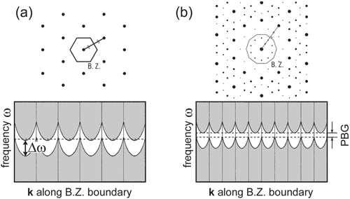
Also in the case of the decagonal quasicrystal in figure (b), we can construct a (pseudo-) Brillouin zone by the use of ten reciprocal-lattice points with relatively large
, and a frequency gap can be formed along its boundary. Here, the amount of vertical shift in the oscillation of the gap frequency range should be smaller because a decagon is more circular than a hexagon. Therefore, the PBG, which is defined as the common gap frequency range, should be formed more easily. From these considerations, it is often claimed that photonic quasicrystals are, in principle, more favourable for PBG formation than conventional photonic crystals. However, this may only be a partial view, as discussed recently by Rechtsman et al [Citation44].
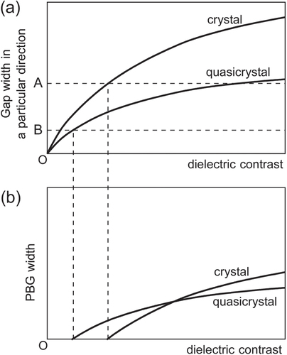
When we compare a photonic crystal and a photonic quasicrystal, we should assume the same dielectric contrast and the same volume ratio between the dielectric and air parts for the two structures. Then, (
: the average of
) should be equal for the two structures. This fact indicates that
is equal for the two structures. Then, the value of
for each of the reciprocal-lattice points forming the zone should generally be smaller in quasicrystals than in crystals, although the possibility of the opposite case being true cannot be excluded, depending on the intensity distribution among the reciprocal-lattice points other than those of interest. If the value of
for each of the reciprocal-lattice points is small, then this indicates that the gap width in a particular direction is small. Figure (a) shows schematically the dependences of the gap width in a particular direction on the dielectric contrast for a crystal and a quasicrystal. The widths for both the crystal and the quasicrystal increase with the increasing dielectric contrast, however the latter is always smaller than the former owing to the reason described above. On the other hand, the PBG, i.e. the gap frequency range that is common to all the directions, emerges when the gap width in a particular direction has surpassed a certain threshold. This threshold should be lower for quasicrystals that have higher rotational symmetry. Consequently, the curves above the threshold values (labelled A for the crystal and B for the quasicrystal) in figure (a) give the PBG widths, which are shown in figure (b). Here, the quasicrystals have larger PBG widths in a region of low dielectric contrast. For this reason, photonic quasicrystals are possibly more favourable for PBG formation than conventional photonic crystals in a region of low dielectric contrast owing to the effect of high rotational symmetry. This has indeed been demonstrated numerically in a 2D example by Rechtsman et al [Citation44].
Figure 10 Illustrations of (a) the dependence of the gap width in a particular direction on the dielectric contrast and (b) the dependence of the PBG width on the dielectric contrast for a crystal and a quasicrystal.
An icosahedral quasicrystal, which possesses icosahedral symmetry, is a unique example of a quasicrystal in 3D. Thus far, little research has been conducted to investigate PBG formation in 3D photonic quasicrystals of this type, and no work has clearly shown the formation of a 3D complete PBG. Dyachenko et al [Citation50] have claimed that a 3D complete gap is formed in a photonic icosahedral quasicrystal consisting of a tetrahedrally coordinated dielectric network. However, their structures are low-order crystal approximants to the quasicrystal, which are more like diamond-related crystals than quasicrystals. Man et al [Citation51] studied the optical properties of a 3D photonic quasicrystal of the 3D Penrose lattice (a typical icosahedral quasicrystalline structure) consisting of dielectric rods, but their structure does not form a complete PBG. We have numerically investigated the formation of a PBG in this type of 3D photonic quasicrystal and found that no complete PBG can be formed at least with a dielectric contrast of or lower. Sutter-Widmer et al [Citation52] have shown experimentally and numerically the formation of band gaps in some 3D ‘phononic’ quasicrystals, but not in 3D photonic quasicrystals.
Light propagation properties
Because the structures of photonic quasicrystals have no periodicity, the Bloch wave vector k cannot be defined, and we cannot draw a photonic band structure such as that shown in figure (a). However, photonic quasicrystals exhibit Bragg scattering of light, and a type of Brillouin zone (a pseudo-Brillouin zone) can be defined, as shown in figure (b). This fact suggests that the notion of the photonic band structure is partially applicable even to photonic quasicrystals, and that some of the applications utilizing photonic bands, as described for photonic crystals in table in section 2.2, may be realizable.
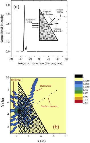
Feng et al [Citation53] have reported that a 2D photonic quasicrystal with a dodecagonal symmetry exhibits negative refraction. Their photonic quasicrystal consists of a quasiperiodic arrangement of dielectric columns with embedded in a styrofoam template. Its microwave transmission spectrum indicated a TM-PBG. They fabricated wedge samples with different wedge angles,
, and investigated the refraction behaviour of TM-mode waves. Figure (a) shows the result for a sample with
at a frequency just above the TM-PBG, where the refracted wave intensity is graphed against the angle of refraction
. A peak is clearly seen at
, corresponding to a negative refractive index of
. This result was fully supported by a numerical simulation using the multiple-scattering theory, as shown in figure (b). The measured
relation indicated that the refractive index of
is almost constant over a wide range of incident angles.
Figure 11 (a) The measured transmission intensity as a function of refractive angle at a
incidence. A wedged sample is illustrated in the inset. (b) The results of a corresponding numerical simulation of wave intensity exhibiting a negative refraction behavior. These figures are taken from [Citation53].
Notomi et al [Citation54] have fabricated photonic quasicrystal lasers and observed coherent lasing action. The quasicrystalline structure they adopted is a 2D Penrose pattern consisting of two types of rhombi. They formed circular holes at the centre of every rhombus (figure (b)). The hole pattern was created in a SiO2 layer on a Si substrate, covered with a laser dye (DCM) embedded in an organic gain medium (Alq3) (figure (a)). A series of samples were fabricated with different quasilattice constants a (the edge length of the tiles). Clear lasing actions were observed, an example of which is shown in figure (c). Emission patterns consisting of bright spots with tenfold rotational symmetry were observed, as shown in figures (a)–(d). All the normalized lasing wavelengths () and emission patterns were shown to match the standing wave conditions of a two-wave coupling:
. This fact indicates that this laser is of a distributed-feedback type, where the Bragg reflections due to quasiperiodic long-range ordering play the role of the feedback. As shown schematically in figures (a) and (b), the density of
with an appreciable value of
in reciprocal space is much higher for quasicrystals than for conventional crystals. As a result, the photonic quasicrystal laser generates much richer variation in the lasing wavelength and emission pattern than a conventional photonic crystal laser. This may be advantageous in applications of this type of laser.
Figure 12 (a) Illustration of the photonic quasicrystal laser. (b) Scanning electron micrograph of the sample. (c) An example of emission spectra. These figures are taken from [Citation54].
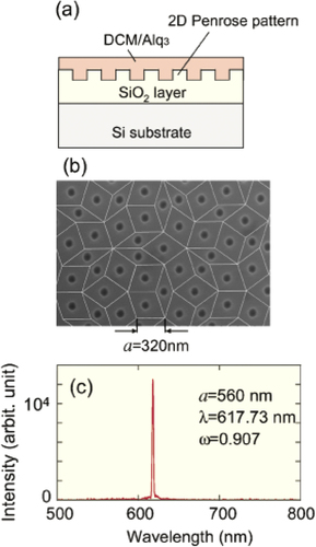
Figure 13 (a)–(d) Spot images of the out-of-plane emission with different conditions as shown in each figure. These figures are taken from [Citation54].
Electronic states in quasiperiodic systems had been theoretically studied since before even the discovery of quasicrystals [Citation39], and some characteristic features, such as a singular continuous energy spectrum and critical electronic states, have been found. The critical states are characterized by , which are intermediate states between the extended states (
) of periodic systems and the localized states (
) of random systems. As described in section 3.2, our understanding of localization phenomena in random systems has progressed significantly by investigating not only those in electronic systems but also those in photonic systems. Similarly, it would be worthwhile to investigate phenomena such as critical states, which are characteristic of quasiperiodic systems, in photonic systems using photonic quasicrystals.
Recently, an interesting mathematical connection between quasicrystals and topological insulators has been reported [Citation55]: (i) quasicrystals exhibit nontrivial topological properties and (ii) these properties are attributed to dimensions higher than that of the quasicrystal. These properties have been demonstrated experimentally in a photonic system consisting of quasiperiodically arranged parallel semiconductor waveguides, where the whole array acts as a 1D quasiperiodic potential for the light, and therefore can be regarded as a kind of 1D photonic quasicrystal. This 1D photonic crystal has been shown to exhibit the topological properties of conventional 2D topological phases. Furthermore, more recently, a 2D quasiperiodic model has been shown to exhibit the topological properties of four-dimensional phases [Citation56].
Concluding remarks
In this final section, we summarize this article, focusing on the two main issues: whether photonic devices of photonic amorphous materials or of photonic quasicrystals can be more efficient than those of photonic crystals, and whether they can exhibit novel properties that conventional photonic crystals can never possess.
In two-dimensional (2D) systems, various types of photonic amorphous and quasicrystalline structures form photonic band gaps (PBG). Disappointingly, the sizes of these PBGs are generally smaller than those of hexagonal photonic crystals, which form the largest PBGs among all the 2D photonic crystals. However, there is a possibility that photonic quasicrystals are more favourable than photonic crystals for PBG formation in a region of low dielectric contrast. It is necessary to clarify in future research whether this expectation is valid in every case.
With regard to three-dimensional (3D) photonic amorphous materials, a structure forming a complete PBG has recently been found, named photonic amorphous diamond (PAD). The PBG in PAD is as clean as that in its crystalline counterpart, photonic crystalline diamond (PCD), with no trace of localized-state formations in the PBG. In relation to this fact, the light-confinement effect by the PBG in PAD is as strong as that in PCD. The width of the PBG in PAD is smaller than that in PCD, which is known to be the best structure exhibiting the largest PBG among all the 3D photonic crystals studied thus far. The mechanism for PBG formation in PAD has not yet been fully clarified. If it can be clarified, then it could lead to the discovery of other amorphous structures with a complete PBG. If some amorphous structure can be shown to form a PBG larger than the largest PBG of photonic crystals, then it would have a big impact on the photonic crystal research community.
For 3D photonic quasicrystals, no structure has been found to form a complete PBG as long as the dielectric contrast is 13/1 or lower. If we can construct a quasicrystalline structure of a tetrahedrally coordinated network, then it would form a complete PBG. This photonic quasicrystal can potentially form a larger PBG than photonic crystals in a low dielectric-contrast region. In general, the PBGs of photonic amorphous materials and photonic quasicrystals are isotropic. This should be more advantageous in various applications, even if their PBG sizes are smaller than those of photonic crystals.
Photonic amorphous materials generally exhibit diffusive light propagation in passbands owing to multiple scatterings of light. In strong scattering systems, the scattering mean free path, , can be very short in a certain frequency region. In PAD,
decreases significantly as the frequency approaches the band edge. Through the use of such short-
regions, we should be able to realize a very thin light diffuser that can completely eliminate the memory of light polarization and wavevector orientation with a thickness comparable to the light wavelength. In general, when
decreases to a threshold value, light localization is realized. In PAD, localized photonic states have been found to form at band edges. Through the use of a lasing action originating from such localized photonic states, so-called random lasers have been realized.
It has been demonstrated that negative refraction and distributed feedback lasers can be realized using the band regions of photonic quasicrystals. They exhibit some peculiar features that conventional photonic crystals do not exhibit, which may be useful in some applications. So far, our understanding of localization phenomena in random systems has progressed significantly as a result of investigating not only those in electronic systems but also those in photonic systems. Similarly, it would be worthwhile to investigate phenomena related to critical states, which are characteristic of quasiperiodic systems, in photonic systems using photonic quasicrystals. The physics of a topological insulator in systems of quasicrystals are certainly an important subject in photonic quasicrystals.
Acknowledgments
We would like to thank S Imagawa (IIS, Univ. Tokyo) and M Notomi (NTT) for their fruitful discussion and valuable comments. We acknowledge the help of Y Kamimura (IIS, Univ. Tokyo) for his help in manuscript preparation.
References
- YablonovitchE 1987 Phys. Rev. Lett. 58 2059 10.1103/PhysRevLett.58.2059
- JohnS 1987 Phys. Rev. Lett. 58 2486 10.1103/PhysRevLett.58.2486
- NotomiM 2010 Rep. Prog. Phys. 73 096501 10.1088/0034-4885/73/9/096501
- ShechtmanDBlechIGratiasDCahnJ W 1984 Phys. Rev. Lett. 53 1951 10.1103/PhysRevLett.53.1951
- JoannopoulosJ DJohnsonS GWinnJ NMeadeR D 2008 Photonic Crystals—Molding the Flow of Light Princeton, NJ Princeton University Press
- PratherD WShiSSharkawayAMurakowskiJSchneiderG J 2009 Photonic Crystals—Theory, Applications, and Fabrication Hoboken, NJ Wiley
- InoueKOhtakaK 2004 Photonic Crystals—Physics, Fabrication and Applications Berlin Springer
- NotomiM 2000 Phys. Rev. B 62 10696 10.1103/PhysRevB.62.10696
- MaldovanMThomasE L 2004 Nature Mater. 3 593 10.1038/nmat1201
- ChanC TDattaSHoK MSoukoulisC M 1994 Phys. Rev. B 50 1988 10.1103/PhysRevB.50.1988
- EconomouE NSigalasM M 1993 Phys. Rev. B 48 13434 10.1103/PhysRevB.48.13434
- ShiLJiangXLiC 2007 J. Phys.: Condens. Matter 19 176214 10.1088/0953-8984/19/17/176214
- JinCMengXChengBLiZZhangD 2001 Phys. Rev. B 63 195107 10.1103/PhysRevB.63.195107
- MiyazakiHHaseMMiyazakiH TKurokawaYShinyaN 2003 Phys. Rev. B 67 235109 10.1103/PhysRevB.67.235109
- RockstuhlCPeschelULedererF 2006 Opt. Lett. 31 1741 10.1364/OL.31.001741
- FlorescuMTorquatoSSteinhardtP J 2009 PNAS 106 20658 10.1073/pnas.0907744106
- EdagawaKKanokoSNotomiM 2008 Phys. Rev. Lett. 100 013901 10.1103/PhysRevLett.100.013901
- ImagawaSEdagawaKMoritaKNiinoTKagawaYNotomiM 2010 Phys. Rev. B 82 115116 10.1103/PhysRevB.82.115116
- EdagawaK 2013 Amorphous Nanophotonics Heidelberg/New York/Dordrecht/London Springer chapter 8
- WootenFWinerKWeaireD 1985 Phys. Rev. Lett. 54 1392 10.1103/PhysRevLett.54.1392
- ChanC TYuQ LHoK M 1995 Phys. Rev. B 51 16635 10.1103/PhysRevB.51.16635
- BarkemaG TMousseauN 2000 Phys. Rev. B 62 4985 10.1103/PhysRevB.62.4985
- ImagawaSEdagawaKNotomiM 2012 Appl. Phys. Lett. 100 151103 10.1063/1.4704182
- ManW NFlorescuMWilliamsonE PHeY QHashemizadS RLeungB Y CLinerD RTorquatoSChaikinP MSteinhardtP J 2013 PNAS 110 15886 10.1073/pnas.1307879110
- ShengP 1995 Introduction to Wave Scattering, Localization, and Mesoscopic Phenomena San Diego Academic
- IshimaruA 1997 Wave Propagation and Scattering in Random Media Piscataway, NJ IEEE Press
- AndersonP W 1985 Phil. Mag. B 52 505 10.1080/13642818508240619
- AryaKSuZ BBirmanJ L 1986 Phys. Rev. Lett. 57 2725 10.1103/PhysRevLett.57.2725
- SoukoulisC MEconomouE NGrestG SCohenM H 1989 Phys. Rev. Lett. 62 575 10.1103/PhysRevLett.62.575
- GarciaNGenackA Z 1991 Phys. Rev. Lett. 66 1850 10.1103/PhysRevLett.66.1850
- WiersmaD SBartoliniPLagendijkARighiniR 1997 Nature 390 671 10.1038/37757
- StorzerMGrossPAegerterC MMaretG 2006 Phys. Rev. Lett. 96 063904 10.1103/PhysRevLett.96.063904
- SchuurmansF J PMegensMVanmaekelberghDLagendijkA 1999 Phys. Rev. Lett. 83 2183 10.1103/PhysRevLett.83.2183
- RivasJ GSprikRLagendijkANoordamL DRellaC W 2001 Phys. Rev. E 63 046613 10.1103/PhysRevE.63.046613
- ScheffoldFLenkeRTweerRMaretG 1999 Nature 398 206 10.1038/18347
- IoffeA FRegelA R 1960 Non-crystalline, amorphous, and liquid electronic semiconductors Progress in Semiconductors GibsonA FBurgessR EKroegerF A London Heywood chapter 4 237
- JohnsonP MImhofABretB P JRivasJ GLagendijkA 2003 Phys. Rev. E 68 016604 10.1103/PhysRevE.68.016604
- van AlbadaM Pvan TiggelenB ALagendijkATipA Phys. Rev. Lett. 66 3132 10.1103/PhysRevLett.66.3132
- SteinhardtP JOstlundS 1987 The Physics of Quasicrystals Singapore World Scientific
- SteurerWSutter-WidmerD 2007 J. Phys. D: Appl. Phys. 40 R229 10.1088/0022-3727/40/13/R01
- ChanY SChanC TLiuZ Y 1998 Phys. Rev. Lett. 80 956 10.1103/PhysRevLett.80.956
- ZoorobM ECharltonM D BParkerG JBaumbergJ JNettiM C 2000 Nature 404 740 10.1038/35008023
- ZhangXZhangZ OChanC T 2001 Phys. Rev. B 63 081105 10.1103/PhysRevB.63.081105
- RechtsmanM CJeongH CChaikinP MTorquatoSSteinhardtP J 2008 Phys. Rev. Lett. 101 073902 10.1103/PhysRevLett.101.073902
- FlorescuMTorquatoSSteinhardtP J 2009 Phys. Rev. B 80 155112 10.1103/PhysRevB.80.155112
- DavidSChelnokovALourtiozJ-M 2000 Opt. Lett. 25 1001 10.1364/OL.25.001001
- RattierMBnistyHSchwoobEWeisbuchCKraussT FSmithC J MHoudreROesterleU 2003 Appl. Phys. Lett. 83 1283 10.1063/1.1600831
- UedaKDoteraTGemmaT 2007 Phys. Rev. B 75 195122 10.1103/PhysRevB.75.195122
- HayashidaKDoteraTTakanoAMatsushitaY 2007 Phys. Rev. Lett. 98 195502 10.1103/PhysRevLett.98.195502
- DyachenkoP NMiklyaevY VDmitrienkoV E 2007 JETP Lett. 86 240 10.1134/S0021364007160047
- ManWMegensMSteinhardtP JChaikinP M 2005 Nature 436 993 10.1038/nature03977
- Sutter-WidmerDNevesPIttenPSainidouRSteurerW 2008 Appl. Phys. Lett. 92 073308 10.1063/1.2884319
- FengZZhangXWangYLiZ YChengBZhangD Z 2005 Phys. Rev. Lett. 94 247402 10.1103/PhysRevLett.94.247402
- NotomiMSuzukiHTamamuraTEdagawaK 2004 Phys. Rev. Lett. 92 123906 10.1103/PhysRevLett.92.123906
- KrausY ELahiniYRingelZVerbinMZilberbergO 2012 Phys. Rev. Lett. 109 106402 10.1103/PhysRevLett.109.106402
- KrausY ERingelZZilberbergO 2013 Phys. Rev. Lett. 111 226401 10.1103/PhysRevLett.111.226401