
Abstract
An environmentally friendly solid-state quantum dot sensitized solar cell (ss-QDSSC) was prepared by combining colloidal SnS QDs as the sensitizer and organic hole scavenger spiro-OMeTAD (2,2′,7,7′-tetrakis-(N,N-di-p-methoxyphenylamine)9,9′-spirobifluorene) as the solid-state electrolyte, and the energy alignment of SnS and TiO2 was investigated. The bandgap of colloidal SnS QDs increased with decreasing particle size from 14 to 4 nm due to an upshift of the conduction band and a downshift of the valence band. In TiO2/SnS heterojunctions, the conduction band minimum (CBM) difference between TiO2 and SnS was as large as ∼0.8 eV; this difference decreased with decreasing particle size, but was sufficient for electron injection from SnS nanoparticles of any size into TiO2. Meanwhile, the sensitizer regeneration driving force, that is, the difference between the valence band maximum (VBM) of SnS and the work function of the electrolyte, showed an opposite behaviour with the SnS size due to a downward shift of the SnS VB. Consequently, smaller SnS QDs should result in a more efficient charge transfer in heterojunctions, revealing the advantages of QDs vs larger particles as sensitizers. This prediction was confirmed by the improved photovoltaic performance of ss-QDSSCs modified with SnS nanoparticles, which peaked for 5–6 nm sized SnS nanoparticles due to the balance between electron injection and sunlight absorption.
Introduction
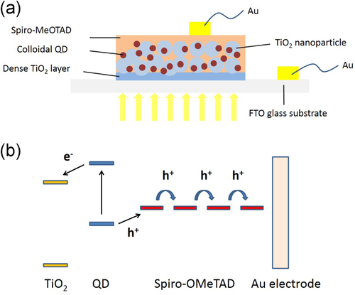
The quantum dot sensitized solar cell (QDSSC), operating similarly to the dye sensitized solar cell (DSSC), has been developed very quickly in the last several years [Citation1–Citation6]. Both devices usually employ a mesoporous layer of titanium dioxide nanoparticles as the backbone, which can then be made photoactive by sensitizing with semiconductor quantum dots using various kinds of methods including chemical bath deposition (CBD), successive ionic layer adsorption and reaction (SILAR), electrophoretic deposition and so on. For QD candidates, II-VI series semiconductors (such as CdS [Citation7, Citation8], CdSe [Citation2], CdS/CdSe [Citation3, Citation4], CdTe/CdSe [Citation6]) based solar cells have been a research hotspot, achieving an efficiency of nearly 5%–6%. Recently, IV-VI series ones with narrower band gap, such as PbS and PbSe, are also surging very quickly, catching up to the efficiency of Cd-based solar cells thanks to their wider sunlight absorption range extended to the near-infrared region [Citation7–Citation10]. However, the severe toxicity of Cd or Pb, which will cause hazardous damage to human bodies, definitely hampers their future application. Consequently, exploration of nontoxic and low-cost semiconductor absorbers with a narrow band gap is necessary and has attracted much attention, among which tin chalcogenides are a good choice. Especially, tin sulfide (SnS) with a direct band gap of 1.3 eV and an indirect band gap of 1.09 eV in bulk has been considered to have huge potential in the fields of near-infrared detectors and solar cells because of its high conductivity and absorption coefficient coupled with the abundant reserves of Sn and S in the Earth [Citation11–Citation16]. Scientists have also made great efforts to construct the SnS sensitized solar cell, especially in the last three years [Citation17–Citation22]. Wang and co-workers synthesized nanocrystalline SnS QDs by the CBD method and designed a structure of ‘FTO/Pt+liquid electrolyte+SnS/TiO2/FTO’, nearly achieving an efficiency of 0.1% [Citation17]. Miyauchi deposited SnS QDs on mesoporous TiO2 by SILAR process, and obtained an efficiency of less than 0.1% [Citation18]. Guo and co-workers used TiC to replace Pt as the counter-electrode and improved the efficiency to about 1%, where corrosive liquid electrolyte based on I−/I3− redox couple was employed [Citation19]. TiO2 nanotube arrays with better charge transport properties than nanoparticles were also employed by Jia and co-workers, where a conversion efficiency of 0.75% and an extremely outstanding open-circuit voltage of 1.08 V under 1 sun illumination were obtained [Citation20]. Overall, despite the broad sunlight absorption spectrum, the SnS-based solar cell still suffers the issue of poor photovoltaic performance. Whether this can be remedied by the proper choice of materials or device structure designing lies in the energy level alignment between SnS and the oxide electrode, which significantly affects the charge separation and recombination efficiency at the interface. Besides, the above reported SnS nanoparticles were all synthesized through a SILAR process or CBD method, where their sizes and energy levels are difficult to control, which hinders investigation of the physical (electrical, optical, etc.) properties of SnS and the TiO2/SnS heterojunctions. Here, instead, the one-pot synthesis method was employed to obtain colloidal SnS QDs with their size precisely controlled, which were then co-graft onto TiO2 film. The energy level alignment between TiO2 and SnS was calculated to clearly uncover the possible charge transfer mechanism among each component of the as-prepared device. More importantly, it should be noted that the reported SnS sensitized solar cells were all based on liquid electrolytes, which encounters the stability problems arising from not only the volatile but also the corrosive nature of the electrolyte. Here, instead, solid-state electrolyte spiro-OMeTAD (2,2′,7,7′-tetrakis-(N,N-di-p-methoxyphenylamine)9,9′-spirobifluorene), a stable organic hole transport material, was used as the hole scavenger. Overall, by elucidating the charge transfer mechanism in the systems employing colloidal SnS nanoparticles with different sizes, we are trying to achieve an environmentally friendly QDSSC with high stability by combining SnS nanocrystals as the sensitizer and the solid-state electrolyte (the structure is exhibited in figure (a)). The expected energy level alignment between different layers for an ideal solar cell is described in figure (b), where the electrons would inject from SnS colloidal nanoparticles into TiO2 and then flow through the conduction band of TiO2 while the holes transport through spiro-OMeTAD to the metal electrodes by hopping. To fabricate this ss-QDSSC, SnS nanocrystals were firstly synthesized under different temperatures with the crystallinity and the phase checked by x-ray diffraction (XRD) and high-resolution transmission electron microscopy (HRTEM). Their sizes have also been calculated, which influenced the optical properties confirmed by UV-Vis-IR absorption measurement. These colloidal SnS nanoparticles were then used to sensitize TiO2 nanoparticles, and x-ray photoelectron spectroscopy (XPS) was employed to figure out the energy level alignment between SnS and TiO2 which was then validated by the photovoltaic performance of the as-prepared solar cells.
Figure 1 Scheme of (a) the structure of SnS ss-QDSSC (the porous TiO2 film consisted of TiO2 nanoparticles), (b) the working principle of the solid-state solar cell with an ideal energy level alignment (the electrons excited in SnS inject into TiO2 and then flow through it). The holes transport through spiro-OMeTAD to the Au electrode by hopping.
Experimental details
Chemicals and materials
All solvents and reagents were used as received. P25 with an average particle size of 21 nm was purchased from Degussa (Germany). Tin(II) chloride (99.9985%), 1-octadecene (ODE; tech. 90%), tri-n-octylphosphine (TOP; 98%), titanium isopropoxide (97%+), oleic acid (OA; 99%), 3-mercaptopropionic acid (3 MPA; 99%), and lithium bis(trifluoromethylsulfon)imide (LiTFSI; 98%+) were purchased from Alfa Aesar. Spiro-OMeTAD (99.9%, Luminescence Technology Corp.) and 4-tert-butylpyridine (TBP; 96%, Aldrich) were used as the solid electrolyte additives. Oleylamine (OLA; 90%) and thioacetamide (99.0%) were obtained from Aladdin. Fluorine-doped tin oxide (SnO2:F, FTO, sheet resistance: 12Ω/sq, Nippon Sheet Glass Co., Japan) was used as the electrode substrate.
Synthesis of SnS nanoparticles
The one-pot synthesis method was employed to obtain colloidal nanoparticles. In a typical synthesis of spherical particles [Citation23, Citation24], 5 ml (15.6 mmol) ODE, 3 ml (6.7 mmol) TOP, 4.5 ml (14.2 mmol) oleic acid and 2 mmol tin(II) chloride were added to a three necked flask, which was then evacuated and flushed with argon at least three times to remove oxygen. The mixture was subsequently heated to the synthesis temperature and then kept at this temperature for approximately 30 min in order to remove the water. Five temperatures were employed, 180 °C, 150 °C, 120 °C, 90 °C and 60 °C. Into this mixture was then quickly injected sulfide precursor, which was prepared by mixing three chemicals of 10 ml (30.4 mmol) OLA, 3 ml (6.7 mmol) TOP and 0.075 g (1 mmol) thioacetamide. After injection, the reaction was kept for 2 min, followed by being quenched under room temperature. The as-prepared colloidal nanoparticles were washed before being used as the sensitizers, for which hexane and acetone were added to the solution, and centrifuged at 4000 rpm with the gravity of 2862 g for 5 min. This operation was repeated twice, and consequently excess organic matter can be removed from the solution. At last, they were dissolved in hexane for the sensitization process.
Dense TiO2 layer preparation
Spiro-OMeTAD and FTO form a contact which is perfectly ohmic, leading to a short-circuit for the solar cell. Therefore, the dense TiO2 layer was employed to act as a blocking layer. 1.42 g titanium isopropoxide was added into 5 g ethanol and stirred for 5 min, which was noted as solution A. 0.02 g HNO3 and 0.35 g H2O were added into 5 g ethanol and stirred for 5 min, which was noted as solution B. Then, Solution B was slowly instilled into solution A, followed by stirring for 15 min. For preparing the dense TiO2 film, 100 μl of the mixture was extracted by pipette and spin-coated on FTO glass substrate at 3000 rpm for 30 s. Then the substrate was put into the oven and annealed at 500 °C for 10 min. The above operation cycle needs to be repeated depending on the required thickness of the dense TiO2 layer. After all the cycles, the substrate was again put into the oven and annealed at 500 °C for 30 min.
Porous titania layer preparation
The porous TiO2 film consisted of TiO2 nanoparticles, for which commercial TiO2 powders (P25) were used. The size of the TiO2 nanoparticles is about 25 nm, which forms pores with a size in the tens of nanometers. Ethyl cellulose was mixed with ethanol at the mass ratio of 1:10. Following this operation, P25 and terpineol was added into the solution at the mass ratio of 18:90:95 (P25: ethyl cellulose solution: terpineol). The ethanol has to be removed from the mixture by distillation, which then turned to a sticky paste and was applied on the dense TiO2 layer surface using a screen-printing method and annealed in the oven. The annealing temperature gradually increased from room temperature to 500 °C and was kept at 500 °C for 30 min [Citation25]. The resultant film thickness of one porous TiO2 layer was ∼3 μm. The effective area of the photoanodes is 0.4 cm2. The TiO2 film needs to be post-treated by TiCl4 solution, for which the substrates were soaked into 0.04 M TiCl4 solution in deionized water for 30 min at 70 °C.
Colloidal SnS nanoparticle sensitization
For co-grafting nanoparticles onto the surface of TiO2, the TiO2 electrodes were first immersed into 10% MPA (3-mercaptopropionic acid) solution in acetonitrile for 24 h. After the substrates were taken out from the MPA solution, they were washed by pure acetonitrile and hexane, and then immediately soaked into the SnS nanoparticles solution for two days. The substrates were then taken out of the solution and washed with hexane, ready for the solar cell fabrication.
Fabrication of SnS ss-QDSSCs
0.17 mol of spiro-OMeTAD, 19 mmol of tert-butylpyridine, 10 mmol of Li[CF3SO2]2N, and 0.3 mmol of N[p-C6H4Br]3SbCl3 were dissolved in 1 mL of dichlorobenzene, which was ready for being used as the hole transport layer. This mixture was then spin-coated on the substrate at 2000 rpm for 30 s. Au counter electrode was built by metal vapor deposition. In detail, 60 mg Au was put in the thermal evaporation system, which was then evacuated to below 4 × 10⁻⁶ Pa. Au was pre-heated by 10 A of current for 30 s and then vaporized by 14 A of current for 40 s. The thickness of the Au layer for all the SnS ss-QDSSCs is nearly 100 nm.
Characterization methods
The crystal structure of SnS was examined by XRD using a Bruker D8 Advance x-ray diffractometer with CuK′α radiation (0.154 06 nm) operating on 40 kV and 40 mA. HRTEM images of SnS nanoparticles were obtained from the Tecnai G2 F20 S-Twin (FEI, USA). The absorbance spectra were obtained by a UV/Vis/NIR spectrophotometer (Lambda 950, Perkin-Elmer, United States). XPS was performed on a PHI Quantera instrument (ULVAC-PHI, Inc. Japan) with AlK'α ( = 1486.6 eV) as the x-ray radiation source, which had been carefully calibrated on work function and Fermi energy level
. All XPS spectra were calibrated by the C1s peak at 284.8 eV from contamination to compensate for the charge effect. The photocurrent density−voltage (J − V) characteristics of the cells were measured with a solar simulator (91 192, Oriel, United States), under an illumination of AM 1.5 (100 mW cm−2). Before photovoltaic performance measurement for solar cells, the simulator was calibrated with the standard Si solar cell (PEC-SI01, Peccell, Japan).
Results and discussion
As described above, the synthesis temperature was altered between 180 °C and 60 °C, among which five points were employed (180 °C, 150 °C, 120 °C, 90 °C, 60 °C separately). The XRD patterns for SnS nanoparticle powders under different temperatures are exhibited in figure , which reveals that the phase of the as-prepared SnS was orthorhombic herzenbergite (a = 11.32 Å, b = 4.05 Å, c = 4.24 Å). There are several phases for SnS, among which the orthorhombic phase was the most stable under room temperature [Citation26, Citation27]. It was also observed that the sample synthesized under 180 °C has good crystallinity similar to that of the bulk one, as a result of its large size (∼13–14 nm shown below in TEM results). With the temperature decreasing, the XRD peaks tended to be broadened due to the decreased size shown also in TEM results.
Figure 2 XRD patterns for SnS nanoparticle powders synthesized at different temperatures (180 °C, 150 °C 120 °C, 90 °C and 60 °C).
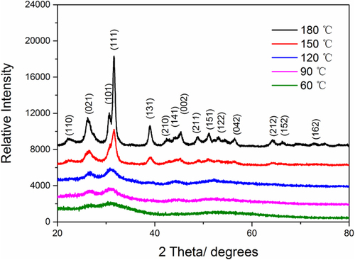
Figure exhibits HRTEM images of SnS nanocrystals synthesized under different temperatures, which showed that the size of SnS nanocrystals has been successfully tuned by changing the synthesis temperature. The average size and its distribution for the SnS QDs were estimated by measuring the diameters. The size ranged between ∼13–14 nm (180 °C) and ∼3–4 nm (60 °C), as was listed in table . It should also be noted that SnS QDs synthesized at lower temperatures might be a mixture of nanocrystalline and amorphous phases, since the crystallinity of the SnS nanoparticles becomes poorer with the size decrease. This could be a factor influencing the photovoltaic performance of the as-prepared solar cells.
Figure 3 HRTEM images of SnS nanoparticles synthesized at different temperatures (a) 180 °C, (b) 150 °C, (c) 120 °C, (d) 90 °C, and (e) 60 °C. (The bar represents 10 nm.)
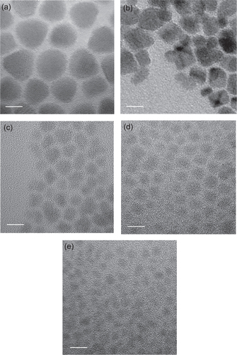
Table 1 The relationship among the synthesis temperature, the size and the band gap of SnS nanoparticles.
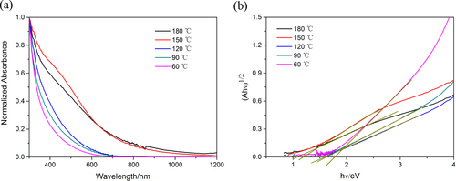
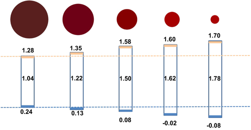
The optical absorption spectra of SnS nanoparticle solutions in hexane is shown in figure (a), which covers the whole visible and also part of the near-infrared region extending to ∼1100 nm for relatively large SnS. By decreasing the synthesis temperature, the absorption threshold is blue-shifted, obviously revealing the quantum confinement effect. The value of the optical band gap for SnS nanoparticles was obtained using the equation for the near-edge absorption and the extrapolation of the linear region of the plot of against photon energy
as shown in figure (b). The corresponding forbidden band gap for SnS synthesized at 180 °C (size: ∼13–14 nm) was ∼1.04 eV, consistent with those reported in the literature for bulk SnS [Citation23]. It could be inferred that SnS nanocrystals with this size or larger would exhibit properties similar to the bulk SnS, which agrees with the XRD pattern shown above. When the size decreased, the band gap was enlarged obviously, which reached up to ∼1.78 eV for the sample with the size of ∼3–4 nm (60 °C). The relationship among the synthesis temperature, the size and the band gap of all the SnS nanoparticles is summarized in table .
Figure 4 (a) Normalized UV-Vis-IR absorption spectra of diluted SnS solutions in hexane synthesized at different temperatures 180 °C, 150 °C, 120 °C, 90 °C, 60 °C. (b) against photon energy
.
To figure out how the band gap was enlarged, XPS measurement was employed by obtaining the valence spectra, where the linear interpolation of the leading edge of the SnS films was executed (shown in figure S1(a); see stacks.iop.org/STAM/15/035006/mmedia) [Citation29, Citation30]. By combining with the band gap results, the conduction band minimum (CBM) was calculated and illustrated in figure . Here, we observed that both the VB’s downward shift and the CB’s upward shift contributed to the band gap enlargement. In the simplest model of quantum confinement, the VB and CB shifts are inversely proportional to the effective mass of holes (mh*) and electrons (me*), respectively [Citation28]. The effective masses of holes and electrons of SnS are both anisotropic in different directions, and a large difference was also observed for
[Citation27], but the shift extent for VB or CB was comparative, which indicates the vital role played by charges along b or c axis for SnS properties as the phase of orthorhombic herzenbergite.
Figure 5 The energy level shift of SnS nanoparticles corresponding to the size change. The numbers inside the rectangle located in the middle represent the band gaps for colloidal SnS with different sizes.
Then the energy level alignment between TiO2 and SnS was evaluated by XPS measurements [Citation29, Citation30]. The Sn3d and Ti2p core levels as well as the VBM
were firstly measured for pure TiO2 and SnS, respectively. These values were measured for the individual films deposited on the FTO glasses. The relative positions of the Sn 3d and Ti 2p core levels were then determined at the interface of the TiO2/SnS film. The valence band offset
at the heterojunction interface can be calculated as follows:
1 where
is the difference between Sn 3d and Ti 2p at the interface of TiO2/SnS film. The CB discontinuities
can then be calculated from
2 where
represents the difference in energy band gap between TiO2 and SnS. As was described in experimental parts, MPA was used as the bifunctional molecule linking SnS and TiO2 together, which was adsorbed on the TiO2 surface before SnS sensitization. It was found that the VB of TiO2 shifted to a more negative (vs normal hydrogen electrode, NHE) energy level (figure. S1(b), Supp. Info. by coating MPA), which is as large as ∼1.21 eV. Here, the band gap for TiO2 is taken as 3.2 eV. By substituting those energy values in equations (Equation1
1 ) and (Equation2
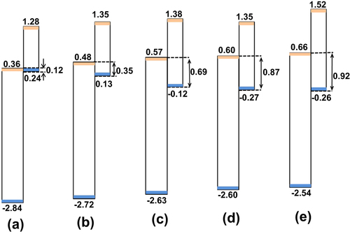
2 ), the VBM and CBM offsets at the interface of the TiO2/SnS heterojunction are calculated, with the schematic representation of the band diagram shown in figure . The detailed values were shown in table S1 (Supp. Info.). Firstly, it was observed that CB and VB of each component both moved slightly when combined into a heterojunction, which is a consequence of the electron interaction between two materials. For instance, both CB and VB of TiO2 moved negatively (vs NHE), for which the shift extent increased gradually with SnS size decrease. In a result, it was predicted that the as-prepared solar cell would exhibit larger and larger VOC, since VOC was decided by the difference between the Fermi level of TiO2 (which upshifts together with the CB of TiO2) and the work function of the electrolyte (which was deemed here to stay the same at ∼4.9 eV vs vacuum). This was proved by the photovoltaic parameters shown below. Secondly, the CBM difference as large as ∼0.8 eV, which is also the electron injection driving force, is sufficient for electron injection from SnS with a different size into TiO2, though it tended to reduce with the decrease of SnS size. This was mainly ascribed to the extraordinarily high CB (small electron affinity) of SnS nanoparticles. In bulk SnS thin film solar cell, theoretical calculation was executed, revealing also a high CB position of SnS compared to the usually used semiconductors (such as CdS, CdTe, Cu2ZnSnS4, etc.) [Citation31]. Actually, this high electron injection driving force may be a waste of energy, leaving a small space (especially for SnS with relatively large size) for the choices of hole scavenger, which should locate between CBM of TiO2 and VBM of SnS. Thirdly, the VBM of SnS was observed to move negatively (vs NHE). Correspondingly, the sensitizer regeneration driving force, which is the difference between the VBM of SnS and the work function of the electrolyte, turned out to be larger and larger with the size decrease. This tendency is favourable for the hole transfer between SnS and the electrolyte, which has been proven by the photovoltaic performances of the as-prepared solar cells shown below.
Figure 6 Schematic representation of the band diagrams between TiO2 and SnS synthesized under different temperatures (a) 180 °C, (b) 150 °C, (c) 120 °C, (d) 90 °C, (e) 60 °C. The numbers marked near the double arrows are the difference between the CBM of TiO2 and the VBM of SnS.
TiO2/SnS heterojunctions were then fabricated into solar cells, with the results of J-V measurement shown in figure . The photovoltaic parameters including open-circuit voltage (VOC), short-circuit current (JSC), fill factor (FF), and the efficiency are listed in table . Due to the possible photoresponse for pure TiO2 under UV light, the device without sensitization was employed as the reference. After SnS deposition, JSC increased in all cells except that based on SnS synthesized at 180 °C, which proved the accuracy of the energy level calculation result shown above. In the working devices, both electron injection from CB of SnS into TiO2 and hole transfer from the VB of SnS into N[p-C6H4Br]3SbCl3 doped spiro-OMeTAD are effective. With SnS size decreasing, the Jsc yield tended to increase, which however decreased for the sample synthesized at 60 °C due to its narrow absorption range. By applying SnS QDs onto the TiO2 surface, VOC was also significantly improved compared to that without sensitization, because of the upshift of the TiO2 Fermi level (vs NHE) after electron injection from SnS to TiO2. More importantly, VOC also tended to increase with the synthesis temperature decrease, ascribed to the negatively shifted CBM of TiO2 by SnS deposition on its surface, which proved the prediction above. The device employing SnS QDs synthesized at 90 °C (∼5–6 nm) exhibited the best photovoltaic performance with an efficiency of 0.01% for ss-QDSSC, which is a comprehensive result of band energy alignment and sunlight absorption. For further improvement of the device properties, to substitute TiO2 into compounds with CBM of more negative potential (vs NHE) was promising in order to avoid energy waste for electron driving force, which is underway in our lab. Besides, the hole mobility is another important factor that limited the efficiency of the solar cell. The mobility of pure spiro-OMeTAD is about 10−5 cm2 V−1 s−1, which could be raised to about 10−3 cm2 V−1 s−1 after doping. However, this is still much lower than the inorganic hole transport materials (HTM). Therefore, to explore new HTM is a promising method to improve the photovoltaic performance of SnS ss-QDSSCs.
Figure 7 J-V characteristics for the solar cells with and without SnS sensitization.
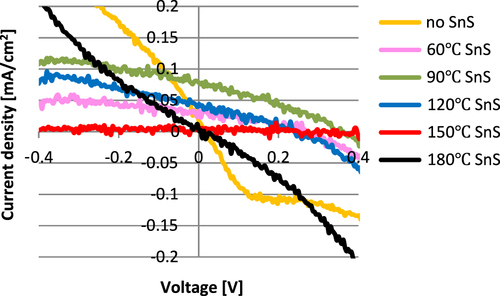
Table 2 Photovoltaic parameters including VOC, JSC, FF and efficiency for the solar cells with and without SnS sensitization.
Conclusions
In summary, SnS nanoparticles with different sizes were obtained by the controllable one-pot synthesis method, where smaller SnS exhibited a more prominent quantum confinement effect and thus the band gap was enlarged leading to the blue-shifted sunlight absorption threshold. XPS results confirmed that the downward shift of VB and the upward shift of CB contributed comparatively to the enlarged band gap for pure SnS QDs. For the TiO2/SnS heterojunction, the energy level alignment, which is vital for the charge transfer mechanism, was carefully calculated. It was confirmed that smaller SnS was more favourable for constructing a solar cell, mainly due to larger hole transfer driving force for SnS regeneration. Besides, the upward shift of TiO2 CB after depositing SnS on its surface also contributed to the enlarged Voc. The photovoltaic performance got a great improvement for the devices with SnS QDs deposition than the one without sensitization thanks to the extended sunlight absorption range by SnS towards pure TiO2, reaching the maximum for that based on SnS QDs synthesized at 90 °C. To further increase efficiency, we are studying hole transport materials and compounds with more negative CBM (vs NHE), to avoid excessive electron injection and thus energy waste.
Acknowledgements
We are grateful to Professor Jiang Tang from Wuhan National Laboratory for Optoelectronics for fruitful discussions, nanocrystal synthesis and physical property characterization. The authors express their gratitude for the support provided by the MOST International S&T Cooperation Program of China (2010DFA64360), the Ministry of Science & Technology, Israel and the Ministry of Science & Technology, P R China: the China–Israel Scientific and Strategic Research Fund No. 7, the 5th round and the 6th round (2013DFG53010), and the National Natural Science Foundation of China (NSFC, 51272126).
References
- KamatP V 2013 J. Phys. Chem. Lett. 4 908 10.1021/jz400052e
- SantraP KKamatP V 2012 J. Am. Chem. Soc. 134 2508 10.1021/ja211224s
- HossainM AJenningsJ RShenCPanJ HKohZ YMathewsNWangQ 2012 J. Mater. Chem. 22 16235 10.1039/c2jm33211f
- LeeY-LLoY-S 2009 Adv. Funct. Mater. 19 604 10.1002/adfm.v19:4
- MoonS-JItzhaikYYumJ-HZakeeruddinS MHodesGGrätzelM. 2010 J. Phys. Chem. Lett. 1 1524 10.1021/jz100308q
- ItzhakovSShenHBuhbutSLinHOronD 2013 J. Phys. Chem. C 117 22203 10 22203–10 10.1021/jp312190x
- HossainM AKohZ YWangQ 2012 Phys. Chem. Chem. Phys. 14 7367 10.1039/c2cp40551b
- LeeJ-WSonD-YAhnT KShinH-WKimI YHwangS-JKoM JSulSHanH 2013 Sci. Rep. 3 1050
- BragaAGimenezSConcinaIVomieroAMora-SeroI 2011 J. Phys. Chem. Lett. 2 454 10.1021/jz2000112
- ZhouNChenG PZhangX LChengL YLuoY HLiD MMengQ B 2012 Electrochem. Commun. 20 97 10.1016/j.elecom.2012.03.032
- SinsermsuksakulPHeoJNohWHockA SGordonR G 2011 Adv. Energy Mater. 1 1116 10.1002/aenm.201100330
- SinsermsuksakulPHartmanKKimS BHeoJSunL ZParkH HChakrabortyRBuonassisiTGordonR G 2013 Appl. Phys. Lett. 102 053901 10.1063/1.4789855
- GhoshBDasMBanerjeePDasS 2008 Sol. Energy Mater. Sol. Cells 92 1099 10.1016/j.solmat.2008.03.016
- ReddyK T RReddyN KMilesRW 2006 Sol. Energy Mater. Sol. Cells 90 3041 10.1016/j.solmat.2006.06.012
- DengZHanDLiuY 2011 Nanoscale 3 4346 10.1039/c1nr10815h
- LiuHLiuYWangZHeP 2010 Nanotechnology 21 105707 10.1088/0957-4484/21/24/245601
- WangYGongHFanB HHuG X 2010 J. Phys. Chem. C 114 3256 10.1021/jp9075756
- MiyauchiM 2011 Chem. Phys. Lett. 514 151 10.1016/j.cplett.2011.08.064
- GuoWShenY HWuM XWangLWangL LMaT L 2012 Chem. Eur. J. 18 7862 10.1002/chem.201103904
- JiaY FYangFCaiF GChengC HZhaoY 2013 Electronic Materials Letters 9 287 10.1007/s13391-013-2216-1
- DeepaK GNagarajuJ 2012 Mater. Sci. Eng. B 177 1023 10.1016/j.mseb.2012.05.006
- TsukigaseHSuzukiYBergerM HSagawaTYoshikawaS 2011 J. Nanosci. Nanotech. 11 1914 10.1166/jnn.2011.3582
- XuYAl-SalimNBumbyC WTilleyR D 2009 J. Am. Chem. Soc. 131 15990 10.1021/ja8086399
- HickeyS GWaurischCRellinghausBEychmüllerA 2008 J. Am. Chem. Soc. 130 14978 10.1021/ja8048755
- ShenH PLinHZhaoLLiuY ZOronD 2013 J. Nanosci. Nanotech. 13 1095 10.1166/jnn.2013.5974
- BurtonL AWalshA 2012 J. Phys. Chem. C 116 24262 10.1021/jp309154s
- VidalJLanySAvezacMZungerAZakutayevAFrancisJTateJ 2012 Appl. Phys. Lett. 100 032104 10.1063/1.3675880
- BrusL 1986 J. Phys. Chem. 90 2555 10.1021/j100403a003
- ChiC FChoH-WTenfHChuangC-YChangY-MHsuY-JLeeY-L 2011 Appl. Phys. Lett. 98 012101 10.1063/1.3533642
- HaleemA M AIchimuraM 2012 J. Appl. Phys. 107 034507 10.1063/1.3294619
- BurtonL AWalshaA 2013 Appl. Phys. Lett. 102 132111 10.1063/1.4801313