
Abstract
SrTiO3 epitaxial growth by molecular beam epitaxy (MBE) on silicon has opened up the route to the monolithic integration of various complex oxides on the complementary metal-oxide–semiconductor silicon platform. Among functional oxides, ferroelectric perovskite oxides offer promising perspectives to improve or add functionalities on-chip. We review the growth by MBE of the ferroelectric compound BaTiO3 on silicon (Si), germanium (Ge) and gallium arsenide (GaAs) and we discuss the film properties in terms of crystalline structure, microstructure and ferroelectricity. Finally, we review the last developments in two areas of interest for the applications of BaTiO3 films on silicon, namely integrated photonics, which benefits from the large Pockels effect of BaTiO3, and low power logic devices, which may benefit from the negative capacitance of the ferroelectric.
1. Introduction
Complex oxides exhibit a wide range of electrical, magnetic, optical and mechanical properties, which may even be coupled. This extraordinary wealth of physical properties offers a huge potential for developing new functionalities in devices that can address societal needs related to health, energy efficiency or information and communication technologies. Ferroelectrics are particularly attractive for their applications in nanoelectronics, communication devices, electro–mechanical systems or sensors. However, in order to exploit their properties, complex oxide integration should be performed in a seamless manner on a semiconductor platform such as silicon or III/V substrates in order to be compatible with the mainstream nanoelectronic industry.
A great variety of complex oxides crystallize in a perovskite-type structure [Citation1]. Tremendous progress has been achieved in the growth of oxides on oxide substrates (such as SrTiO3, LaAlO3, scandates, Al2O3, MgO…) in the past 15 years. Unit cell control (∼4 Å) of the growth can now be achieved. New phenomena arising from interfaces have emerged [Citation2–Citation5]. Progress in characterization techniques and modeling (density functional theory (DFT)) have allowed the study of physico-chemistry and mechanisms involved at the nanoscale and have resulted in a better understanding of the effect of size, strain and boundaries conditions on the properties of complex oxides.
Integrating a perovskite oxide epitaxially on silicon is much more difficult and is still in its infancy, particularly regarding practical devices. One major difficulty for the epitaxy lies in the necessity to avoid the formation of an amorphous SiO2 interfacial layer in the first stages of the growth. The first direct epitaxy of a perovskite (SrTiO3) on silicon was realized by molecular beam epitaxy (MBE) in 1998 [Citation6]. MBE provides unique advantages to precisely construct, almost atom by atom, the oxide/semiconductor interface. Although this breakthrough achievement showed promise in integrating—in a monolithic way—oxides on a semiconductor platform, only a few successes have been reported in the past 15 years [Citation7].
In this contribution to the focus issue on ‘Properties and Applications of Perovskites’, we discuss the monolithic integration of complex oxides on semiconductors by MBE. We will illustrate the particular case of the ferroelectric BaTiO3 compound. We review the work in the literature as well as our own work. The crystalline structure and the ferroelectric properties of BaTiO3 heterostructures on Si, Ge and GaAs are presented. Finally, an overview of perspectives and recent progress in ferroelectric oxide integration on semiconductors for low power logic devices and integrated photonics is provided.
2. MBE of complex oxides: a brief introduction to the technique
MBE was originally developed to epitaxially grow III–V compound semiconductors on a crystalline substrate [Citation8, Citation9]. It allows a control almost atom by atom of the growth in ultrahigh vacuum conditions. Progress in the MBE of oxides as well as in other deposition techniques took off in the late 1980s, after the discovery of the high-Tc superconductor YBa2Cu3O7-δ. This implied the design of dedicated metal-oxide growth MBE chambers. MBE of crystalline oxides on silicon and on other semiconductor substrates has been developed in the late 1990s when the first epitaxy of SrTiO3 on Si was demonstrated [Citation6]. This research benefited from the huge amount of efforts triggered by the microelectronic industry on the search for high-permittivity (high κ) oxides as a replacement to SiO2 (or SiON) gate oxide in complementary metal-oxide–semiconductor (CMOS) field-effect transistors.
In the MBE of complex metal oxides, Knudsen effusion cells commonly used to evaporate the metals (Ba, Sr, Ti…) are focused onto a heated substrate under ultrahigh vacuum conditions (typically 10−10–10−9 Torr). In the case of refractory elements, such as Ti, various means of evaporation have been reported: effusion cells, e-beam gun evaporation, Ti-Ball sublimation source [Citation10] and metal-organic vapor source [Citation11, Citation12]. Metal organic sources used in metalorganic chemical vapor deposition [Citation13] such as titanium tetra isopropoxide Ti(OCH3H7)4 have been proposed in order to increase by several orders of magnitude the vapor pressure of Ti as compared to solid source and to have a beam flux that is relatively unaffected by the presence of oxygen in the chamber [Citation12]. A wide window of growth parameters with self-regulating stoichiometry has been reported for SrTiO3 films grown using such a hybrid approach combining a conventional Sr effusion cell with a metalorganic precursor source for Ti [Citation12].
For a given compound, deposition occurs by alternating the individual flux by means of shutters or by co-directing all fluxes simultaneously towards the substrate. Either molecular oxygen or atomic oxygen generated by a plasma source is typically used to provide the necessary oxygen to form the oxide. The oxygen pressure ranges typically from the 10−8 to 10−5 Torr. The background oxygen pressure plays a major role on the final stoichiometry, crystalline orientation and roughness of the films, as we will show later.
The reactivity of metal elements (in the chamber and in the sources) with the ambient oxygen (typically in the high 10−8–10−5 Torr range) makes the control of the beam fluxes, and therefore composition, difficult. This is actually a major issue in the MBE of multicomponent oxides, which can usually accommodate a large range of non-stoichiometric composition. Indeed the physical properties of complex oxides are strongly dependent on the cationic and oxygen stoichiometry. Moreover, composition deviation may lead to the formation of spurious phases. A quartz crystal microbalance may be used to measure the flux of each atomic beam at the position of the substrate but it does not allow simultaneous monitoring of each flux (it is not element specific) and cannot be employed for in situ control of the composition. In situ monitoring techniques have been proposed for composition control of multi-element oxides [Citation14]. Among them, reflection high-energy electron diffraction (RHEED) is commonly used and has proven to be an effective in situ and real-time diagnostic tool. A review article is proposed in [Citation15] for the use of RHEED during complex oxide growth. It allows one to follow in real time the crystallinity of the deposited film and to adjust in real time the composition by tuning the impinging fluxes when additional spots originating from spurious phases are observed on the RHEED pattern.
Haeni et al [Citation16] have proposed to use RHEED oscillations, both their shape and intensity, to control in real time the composition of multicomponent oxides such as SrTiO3. They reported a control to within 1% of Sr:Ti ratio by monitoring the shuttered RHEED oscillations as the substrate surface is sequentially exposed to the Sr or Ti fluxes. This precise control of monolayer (ML) doses of Sr and Ti has been used to successfully grow the first five members of the Srn+1TinO3n+1 Ruddlesden–Popper phases [Citation17, Citation18].
Various complex oxides have been grown by MBE. As mentioned, the development of oxide MBE started after the discovery of the high Tc cuprate superconducting compounds [Citation19–Citation28]. Since then, a variety of multiple-cation oxides have been epitaxially deposited by MBE on oxide substrates: SrTiO3, Ruddlesden–Popper phases, Bi4Ti3O12, Ba(Sr)TiO3, SrVO3, GdTiO3, BiFeO3, LaAlO3, PbTiO3, LaCrO3, SrCrO3−δ, La1−xSrxFeO3, LaTiO3.5, La2Zr2O7, LaNiO3, La2NiO4, LaSrAlO4, and superlattices e.g. BaTiO3/SrTiO3 or PbTiO3/ SrTiO3 to name only a few compounds and groups [Citation29–Citation54]. On Si substrates, epitaxial SrTiO3 films are used as templates to grow a variety of complex oxides. BaTiO3 has been the most studied one by MBE. Apart from this compound, relatively few complex oxides (perovskite, spinel, pyrochlore phases…) have been grown by MBE on Si [Citation55–Citation62]. In many cases, the epitaxial growth on the template layers is completed using other deposition techniques such as pulsed laser deposition, sputtering, chemical vapor deposition or atomic layer deposition, as reported in [Citation64–Citation69] for BaTiO3.
A review of crystalline oxides on silicon is provided in [Citation7]. The paper by Baek and Eom [Citation63] gives a recent review of the epitaxial integration on silicon using SrTiO3 templates of the multiferroic BiFeO3, of the relaxor Pb(Mg1/3Nb2/3)O3–PbTiO3 (PMN-PT) and of LaAlO3/SrTiO3 heterostructures for 2D electron gas creation at their interface.
In the following, we focus on the MBE of the ferroelectric compound BaTiO3 on silicon, germanium and gallium arsenide and on the related crystalline and ferroelectric properties.
3. MBE of BaTiO3 on semiconductors: growth and crystalline structure
BaTiO3 is a prototypical ferroelectric perovskite oxide, with a Curie temperature of 120 °C. The ferroelectric tetragonal structure has lattice parameters of a = 3.994 Å and c = 4.0335 Å with space group P4mm (ICDD #83–1880) and the cubic paraelectric one has a lattice parameter of 4.006 Å with space group Pm-3m (ICDD #79–2263). The polarization is aligned along the c-axis of the tetragonal lattice. The tetragonality ratio c/a is 1.01, which is smaller than in Pb-based ferroelectrics such as PbTiO3 (c/a = 1.04). BaTiO3 is an attractive ferroelectric for nanoelectronic, energy harvesting and photonic applications as will be discussed later in this article. It is a lead-free compound, which is an advantage regarding European regulation and industrial clean room compatibility.
While most MBE depositions of BaTiO3 on a semiconductor have been carried out on silicon, there is a growing interest in Ge and GaAs.
Silicon is the major semiconductor industry substrate. Current CMOS technologies are based on silicon wafers with size up to 300 mm and technologies on 450 mm wafer size are under development. Germanium (also a group IV semiconductor) is of high interest for field-effect transistors with p-type channel (p-FETs) due to the higher mobility of holes as compared to Si. Biaxially strained SiGe channels on Si have also recently attracted much attention for p-FETs. Both Si and Ge have a diamond structure with lattice parameter of 5.431 Å and 5.658 Å respectively. They form a solid solution Si1−xGex in the entire composition range (0 ≤ x ≤ 1).
The III–V gallium arsenide semiconductor has higher electron mobility than Si, which makes it attractive for n-FETs. It is today extensively studied as a channel for advanced CMOS technologies. GaAs has also a wider band gap than Si making it highly resistive if undoped. It is also more resistive to heat and radiation damage. It is suited for many applications such as high frequency devices in communications or such as microwave and millimeter wave integrated circuits. Another advantage of GaAs is its direct band gap, which is of interest for optical applications. GaAs has a zinc blende structure with a lattice parameter of 5.653 Å.
BaTiO3 deposition is mostly performed using an oxide template since the direct epitaxy on semiconductors would result in a high defect density or in a non-appropriate film orientation. We thus describe the direct growth of SrTiO3 epitaxial films on semiconductors when relevant and their use for the epitaxial growth of BaTiO3.
In the following, BaTiO3 crystalline domains with respectively the c-axis or the a-axis of the tetragonal cell being out-of-plane relatively to the substrate (001) plane are denoted respectively c-domains and a-domains.
3.1. MBE of BaTiO3 on silicon
The lattice mismatch (aSi–aBTO)/aBTO, between BaTiO3 and Si(001) is about 4%, which is quite large and tends to favor a-axis growth when BaTiO3 is directly grown on Si [Citation70]. Moreover, the large mismatch of the thermal expansion coefficients between Si (α = 2.6 × 10⁻⁶ K−1) and BaTiO3 (α = 9 × 10⁻⁶ K−1) leads to an in-plane biaxial tensile strain exerted on BaTiO3 upon cooling, which favors a-axis growth. In order to obtain c-axis oriented BaTiO3 films on silicon, a buffer layer that exerts a biaxial compressive in-plane strain should be used to overcome the biaxial tensile in-plane strain during cooling to room temperature [Citation71]. SrTiO3 has been widely used for such a purpose.
3.1.1. SrTiO3 epitaxial templates on Si
The pioneering work of McKee and co-workers [Citation6] opened up the route to the epitaxial growth of perovskite-type compounds on silicon and more generally to any oxide that could be epitaxially grown on bulk SrTiO3 substrates.
SrTiO3 is probably the most investigated epitaxial oxide on silicon [Citation7, Citation72–Citation100]. Many studies have been directed towards understanding the crystalline and electronic structure of the film and of its interface with Si (or SiO2).
The epitaxial growth is realized by passivating the clean Si(001) 2 × 1 reconstructed surface by ½ of a ML of Sr. The Sr atoms are positioned between the Si dimers and prevent the surface from oxidizing. The native SiO2 can be in situ thermally removed at high temperature; the clean Si (001) surface is then passivated by dosing the Sr metal to ½ ML. SiO2 can also be removed using a strontium-assisted deoxidation process in which Sr acts as a catalyst to desorb the native oxide [Citation74]; in this case, once SiO2 is fully desorbed, more Sr is deposited until a 2 × 1 reconstructed surface appears on the RHEED, indicating the passivation of the Si(001) surface with ½ ML Sr coverage. The subsequent growth of SrTiO3 can be performed in different ways. The first few MLs have to be grown at low temperature in order to avoid the oxidation of the interface.
Commensurate SrTiO3 thin films may be grown on Si(001) using a sequential process named ‘kinetically controlled sequential deposition process’ [Citation75, Citation82]. The growth proceeds by alternating a low temperature deposition (∼200–300 °C) of 1–3 ML of a mainly amorphous Sr–Ti–O compound under an oxygen pressure of typically 10−8–1.5 × 10⁻⁷ Torr, followed by an annealing step at higher temperature (580–700 °C) in ultrahigh vacuum conditions (<5 × 10⁻⁹ Torr) to crystallize the SrTiO3 phase. When grown in such conditions, there is no interfacial SiO2 oxide formed and SrTiO3 films have in plane lattice parameter commensurate to the Si 1 × 1 lattice. Relaxation occurs for ∼5 ML. Ferroelectricity in such ultrathin compressively strained films has been reported [Citation89].
The SrTiO3 deposition may also be performed by growing at a higher temperature after the first few MLs of SrTiO3 have been grown, with a low temperature growth/high temperature post-anneal. In this case, the higher growth temperature (>450 °C) under oxygen results in an amorphous SiO2 interfacial layer due to oxygen diffusion through the film down to the interface with silicon. Since this amorphous layer occurs after the direct epitaxy of SrTiO3 on Si, it does not disrupt the epitaxy of the SrTiO3 film and subsequent oxide growth. The epitaxial relationship between SrTiO3 and Si, due to the lattice mismatch, is: [100]SrTiO3//[110]Si and (001)SrTiO3//(001)Si.
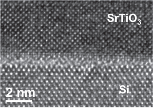
In figure , we show a high resolution transmission electron microscopy (TEM) image of a SrTiO3 film deposited on Si substrate at a temperature of 400 °C under an oxygen partial pressure of P(O2) = 5 × 10⁻⁸ Torr followed by a crystallization step at 460 °C for 20 min under ultrahigh vacuum. We used a rapid cooling down procedure followed by a plasma anneal at 200 °C for 40 min in order to minimize the SiO2 regrowth while providing oxygen to the SrTiO3 lattice.
Figure 1. High-resolution TEM image of a SrTiO3 thin film deposited on Si (001) substrate by MBE.
Choi et al showed that the SiO2 interfacial layer thickness increased during post-deposition annealing as P(O2) and/or annealing time were increased (annealing at 650 °C under P(O2) from 2 × 10⁻⁷ to 1 × 10⁻⁵ Torr) [Citation96] and that it can be used to tune the strain relaxation of the SrTiO3 layer. Before annealing, the SrTiO3 layers are expanded in-plane due to the bi-axial tensile strain exerted by Si during cooling down. As the oxygen partial pressure is increased during the post-deposition anneal, the SrTiO3 lattice parameters evolve towards those of a cubic structure, which is concurrent to the SiO2 interlayer thickness increase (figure ). Strain can be tuned in the SrTiO3 films within half a per cent, which can be useful to adapt the lattice constants to the oxide to be grown on top [Citation96].
Figure 2. (a) In-plane and out-of-plane lattice constants and (b) SiO2 thickness as a function of oxygen partial pressure. All films were annealed at 650 °C for 30 min in different oxygen environments. From figure 5 in [Citation96]. Reprinted with permission from M Choi et al 2012 J. Appl. Phys. 111 064112. Copyright 2012, AIP Publishing LLC.
![Figure 2. (a) In-plane and out-of-plane lattice constants and (b) SiO2 thickness as a function of oxygen partial pressure. All films were annealed at 650 °C for 30 min in different oxygen environments. From figure 5 in [Citation96]. Reprinted with permission from M Choi et al 2012 J. Appl. Phys. 111 064112. Copyright 2012, AIP Publishing LLC.](/cms/asset/f6aab635-0f3e-40a2-9505-30b72a553937/tsta_a_11661311_f0002_oc.jpg)
Thick SrTiO3 films (100 nm) grown by MBE and annealed at high temperature (900 °C) exhibit a full width at half maximum (FWHM) of the 002 rocking curve much narrower than the one of a bulk single crystalline substrate (the quality of which may, however, vary considerably depending on the quality of the original crystal) [Citation90]. A TiO2-terminated surface similar to the one typically prepared on bulk single crystalline SrTiO3 substrates could be obtained by buffered HF etching of the annealed films [Citation90]. This procedure requires, however, thick films since interfacial reactions occur at high temperatures. On thinner 1–4 nm SrTiO3 templates on Si, such a post-deposition annealing at 900 °C is not feasible. The surface may be TiO2 terminated by switching off the Sr beam and properly dosing the Ti flux.
3.1.2. MBE of BaTiO3 on SrTiO3-buffered Si
In their pioneering work [Citation71], the group of Schlom used the solid solution Ba1−xSrxTiO3 as a buffer and could obtain fully c-axis oriented BaTiO3 films, while previous attempts to grow BaTiO3 on silicon had lead to a-axis films. Both the Ba0.7Sr0.3TiO3 buffer and the BaTiO3 films were grown by MBE. A thickness of about 10 nm was estimated for the buffer to be relaxed, which was the condition to obtain c-axis BaTiO3 growth. In these conditions, a 10 nm BaTiO3 film was commensurate with the buffer (30 nm) and had an in-plane lattice parameter of 3.9996 ± 0.0005 Å, indicating that the film was predominantly c-axis oriented. This result was corroborated by optical second harmonic generation measurements. Shortly after, the group of Wessels [Citation101] demonstrated the growth of c-axis BaTiO3 using a 5 ML SrTiO3 template (∼2 nm). By varying the film thickness, they observed that the BaTiO3 growth started as pseudomorphic and that strain relaxation occurred at a critical value of 10 ML (∼4 nm). The out-of-plane lattice parameter was found to be fully relaxed at about 30–40 nm. They observe a mixed a- and c-oriented domain structure and the values extracted from a θ/2θ x-ray diffraction scan were a = 4.01 Å and c = 4.05 Å. Niu et al [Citation102] reported the growth of a 40 nm BaTiO3 fully c-axis film on SrTiO3-buffered (5 nm thick) Si substrate, with lattice parameters of a = 3.978 Å and c = 4.057 Å (c/a = 1.020).
In [Citation103], BaTiO3 films of thickness in the range 1.6–40 nm were studied with a 3.9–6.2 nm SrTiO3 template. X-ray diffraction and high-resolution TEM images indicated a pseudomorphic growth for the ultrathin 1.6 nm films. Films of thickness 8–10 nm were fully c-axis oriented with lattice parameters values close to the bulk ones (a = 3.993 Å and c = 4.038 Å with c/a = 1.011) while 16 and 40 nm films were composed of mixed c- and a-oriented domains. The local crystalline structure was determined by geometrical phase analysis (GPA) of high-resolution scanning transmission electron microscopy (HR-STEM) images. Figure shows the lattice parameter maps along the [100] and [001] as well as the lattice parameter profiles as a function of distance from the amorphous interfacial layer determined for a 16 nm BaTiO3 film deposited on a 3.9 nm SrTiO3 buffer on Si. In figure (c), the out-of-plane lattice parameter is larger than the in-plane one throughout the BaTiO3 thickness, indicating fully c-axis oriented domain. In other regions of the film (figure (d) orange profile), the film grows first c-axis and switches to a-axis after ∼4.0–4.5 nm. It is noticeable that the in-plane parameter increases continuously and therefore the switch from c- to a-domains is continuous. The tetragonality is maximum close to the interface with the SrTiO3 template layer (e.g., a = 3.970 Å and c = 4.065 Å, c/a = 1.023) and decreases throughout the film thickness. Similar results were obtained on thicker films, in which the proportion of a-axis domains becomes predominant. Typical local lattice parameters determined by GPA were a = 4.01 Å and c = 4.05 Å (c/a = 1.010) for a 40 nm thick film. These values are similar to those reported in [Citation101]. Edge dislocations were observed at the SrTiO3/BaTiO3 interface. The numerous profiles performed on different areas of each sample suggested that the lateral scale of the c- and a-domains, when in coexistence, was similar or smaller than the 10–20 nm lateral distance between dislocations.
Figure 3. Strain analysis in a 16 nm BaTiO3/SrTiO3/amorphous interfacial layer (silicate and SiO2) stack. (a), (b) Maps of in-plane (a) and out-of-plane (b) lattice parameters determined from GPA of HR-STEM images. (c)–(e) Lattice parameter profiles as a function of distance d from the interface between the amorphous interfacial layer and the crystalline SrTiO3 layer, determined by averaging data from the black (c), orange (d) and blue areas (e) in (a) and (b). Adapted from figure 2 in [Citation103]. Reprinted by permission from Macmillan Publishers: C Dubourdieu et al 2013 Nat. Nanotechnol. 8 748, copyright 2013.
![Figure 3. Strain analysis in a 16 nm BaTiO3/SrTiO3/amorphous interfacial layer (silicate and SiO2) stack. (a), (b) Maps of in-plane (a) and out-of-plane (b) lattice parameters determined from GPA of HR-STEM images. (c)–(e) Lattice parameter profiles as a function of distance d from the interface between the amorphous interfacial layer and the crystalline SrTiO3 layer, determined by averaging data from the black (c), orange (d) and blue areas (e) in (a) and (b). Adapted from figure 2 in [Citation103]. Reprinted by permission from Macmillan Publishers: C Dubourdieu et al 2013 Nat. Nanotechnol. 8 748, copyright 2013.](/cms/asset/f0153a45-0b9f-4d59-b74f-3c91106c3b08/tsta_a_11661311_f0003_oc.jpg)
In the work by Abel et al [Citation104], a MBE 8 nm BaTiO3 film grown on 4 nm SrTiO3 was found to be fully c-axis oriented as well, with an out-of-plane lattice parameter close to the bulk c value. Similarly, in [Citation105], we observed fully c-axis oriented films for 7 nm BaTiO3 with lattice parameters a = 3.996 Å and c = 4.027 Å. Droopad et al [Citation106] reported c-axis orientation for a 8 nm film grown on a strained 2 ML (∼0.8 nm) SrTiO3 buffer, with an out-of-plane parameter c = 4.032 Å. Lattice parameters reported by various groups in this thickness range (7–8 nm) are in good agreement [Citation103–Citation106].
Thicker films of 80–130 nm were studied for photonics applications as they are of potential interest for integrated electro–optic modulators and other photonic devices [Citation107, Citation108]. A 130 nm thick BaTiO3 film was grown on 4 nm thick SrTiO3 template and was fully a-axis relaxed with lattice parameters a = 3.997 ± 0.005 Å and c = 4.032 ± 0.005 Å (c/a = 1.009) [Citation107]. For 80 nm BaTiO3 film on 8 nm SrTiO3-buffered silicon-on-insulator (SOI) substrates, an out-of-plane lattice constant of 3.998 Å and an average in-plane lattice constant of 4.03 Å were reported, indicating relaxed a-axis film as well [Citation108]. Atomic force microscopy (AFM) showed a smooth surface with a root-mean square (rms) roughness as low as 0.4 nm (one unit cell) [Citation108]. Such thick films are a-axis oriented due to the tensile in-plane biaxial strain applied by the substrate during cooling down.
The critical thickness at which the orientation switches from c- to a-axis is determined by the competing influence of compressive stress from epitaxy and tensile stress from thermal expansion. Among other crucial influence might be the SrTiO3 buffer thickness and surface quality and the composition of the BaTiO3 film. Slight cationic off-stoichiometry may result in oxygen vacancies and structural defects that impact the lattice parameters and strain state [Citation32]. Deposition conditions such as oxygen background pressure or deposition temperature have a major influence on the film growth and may impact the film composition. We have shown [Citation105] that oxygen partial pressure P(O2) has a strong effect on the morphology and crystalline orientation of 16–18 nm films. Increasing P(O2) in the range 1 × 10⁻⁷–3 × 10⁻⁶ Torr leads to an increase of the surface roughness as shown in figures (a)–(d) by the RHEED patterns and AFM images. The RHEED patterns for films grown at (1–5) × 10−7 Torr exhibit well-contrasted streaky lines as expected for a 2D growth. Starting at 2 × 10⁻⁶ Torr, partial or fully spotty patterns are recorded, which characterizes a rougher surface. From AFM, the rms increases from 0.35 nm (1 × 10⁻⁷ Torr) to 0.82 nm (3 × 10⁻⁶ Torr). X-ray diffraction indicated that increasing P(O2) promotes the growth of a-axis grains. Films grown at 1 × 10⁻⁷ Torr were fully c-axis oriented. With increasing P(O2), the out-of-plane parameter was found to decrease while the in-plane parameter increases. The FWHM of the rocking curves performed on the 002 peak (shown in figures (e)–(f)) is of 1.5° and 2.9° at 5 × 10⁻⁷ and 2 × 10⁻⁶ Torr respectively (our lowest FWHM for a 002 rocking curve measured for ∼16 nm films is of the order of 0.7°). The ratio of the out-of-plane/in-plane parameters is lower than 1 for pressures equal or larger than 2 × 10⁻⁶ Torr [Citation105]. This trend was also reported for laser MBE-grown BaTiO3 films on SrTiO3 bulk substrates [Citation109]. The effect of P(O2) on the cationic Ba/Ti composition and on its impact on the crystalline orientation should be further investigated.
Figure 4. (a)–(d) RHEED patterns recorded along the [100] azimuth during BaTiO3 growth at 450 °C under an oxygen pressure of (a) 1 × 10⁻⁷ Torr, (b) 5 × 10⁻⁷ Torr, (c) 2 × 10⁻⁶ Torr, (d) 3 × 10⁻⁶ Torr and corresponding AFM images of the film surfaces. (e)–(f) Rocking curve measured on the 002 peak for the films grown at (e) 5 × 10⁻⁷ (FWHM = 1.5°) and (f) 2 × 10⁻⁶ Torr (FWHM = 2.9°).
![Figure 4. (a)–(d) RHEED patterns recorded along the [100] azimuth during BaTiO3 growth at 450 °C under an oxygen pressure of (a) 1 × 10⁻⁷ Torr, (b) 5 × 10⁻⁷ Torr, (c) 2 × 10⁻⁶ Torr, (d) 3 × 10⁻⁶ Torr and corresponding AFM images of the film surfaces. (e)–(f) Rocking curve measured on the 002 peak for the films grown at (e) 5 × 10⁻⁷ (FWHM = 1.5°) and (f) 2 × 10⁻⁶ Torr (FWHM = 2.9°).](/cms/asset/6d2590ca-7ba6-4453-ac36-e30bc7c31c43/tsta_a_11661311_f0004_oc.jpg)
Oxygen stoichiometry is a major issue in MBE since oxidizing atmosphere and ultrahigh vacuum conditions are antagonistic. BaTiO3 is grown either using molecular O2 or atomic oxygen often created by a radio-frequency plasma. A post-deposition annealing might be performed in order to ensure sufficient oxidation of the films in order to reduce leakage currents and favor a stable ferroelectric polarization. Another issue related to the oxidation of the film is the SiO2 regrowth, which—depending on the application—might be detrimental for the properties. Thickness values of ∼3 nm [Citation104] to ∼3.6 nm [Citation103, Citation106] have been shown by TEM. Growth conditions and post-deposition annealing conditions have actually a strong impact on the interfacial SiO2 regrowth, as reported in [Citation105] and illustrated in figure . We performed post-deposition annealing either in molecular O2 or in an oxygen plasma (typically 400 W). Figure (a) shows an interfacial layer of ∼2.5–3.0 nm for films grown at 450 °C under molecular O2 and slowly cooled down (10 °C min−1) to room temperature under P(O2) = 1 × 10⁻⁵ Torr. For the same growing temperature and P(O2) conditions during the growth but a different post annealing using a rapid cooling down under ultrahigh vacuum followed by a plasma anneal at 200 °C for 40 min, the SiO2 layer is only ∼0.7–1.0 nm (figure (b)). In the same post-deposition annealing conditions but at a growing temperature of 525 °C, the SiO2 is of ∼1.7 nm as indicated in figure (c). The use of an atomic oxygen plasma at low temperature clearly minimizes the interfacial layer regrowth [Citation105]. A detailed study of the defect structure in the SrTiO3 buffer and BaTiO3 film is underway to determine the impact of the processing conditions.
Figure 5. High resolution transmission electron microscopy images of BaTiO3/SrTiO3 stacks grown under P(O2) = 1 × 10⁻⁷ Torr for different temperatures and post-deposition process. (a) 450 °C—slow cooling down procedure at P(O2) = 1 × 10⁻⁵ Torr, (b) 440 °C—rapid cooling down under ultrahigh vacuum (UHV) followed by annealing under an oxygen plasma (1 × 10⁻⁵ Torr) for 40 min, (c) 525 °C—rapid cooling down under UHV followed by annealing under an oxygen plasma (1 × 10⁻⁵ Torr) for 40 min. A SiO2 interfacial layer between Si and SrTiO3 is formed upon SrTiO3 annealing and BaTiO3 growth and its thickness depends on the cooling down conditions. Horizontal dotted lines are only to guide the eyes. From figure 6 in [Citation105]. Reprinted with permission from L Mazet et al 2014 J. Appl. Phys. 116 214102. Copyright 2014, AIP Publishing LLC.
![Figure 5. High resolution transmission electron microscopy images of BaTiO3/SrTiO3 stacks grown under P(O2) = 1 × 10⁻⁷ Torr for different temperatures and post-deposition process. (a) 450 °C—slow cooling down procedure at P(O2) = 1 × 10⁻⁵ Torr, (b) 440 °C—rapid cooling down under ultrahigh vacuum (UHV) followed by annealing under an oxygen plasma (1 × 10⁻⁵ Torr) for 40 min, (c) 525 °C—rapid cooling down under UHV followed by annealing under an oxygen plasma (1 × 10⁻⁵ Torr) for 40 min. A SiO2 interfacial layer between Si and SrTiO3 is formed upon SrTiO3 annealing and BaTiO3 growth and its thickness depends on the cooling down conditions. Horizontal dotted lines are only to guide the eyes. From figure 6 in [Citation105]. Reprinted with permission from L Mazet et al 2014 J. Appl. Phys. 116 214102. Copyright 2014, AIP Publishing LLC.](/cms/asset/9f9eabcd-7a78-457e-9ef4-84d3fb5f84a4/tsta_a_11661311_f0005_oc.jpg)
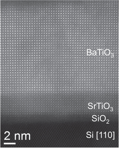
Figure is a STEM high-angle annular dark field (HAADF) image of the sample shown in figure (b), illustrating the high crystalline quality of the perovskite stack and sharp BaTiO3/SrTiO3 and SiO2/SrTiO3 interfaces. The BaTiO3 film is coherently strained to the SrTiO3 buffer layer with no dislocations observed at the interface or in the film thickness.
Figure 6. Scanning transmission electron microscopy high-angle annular dark field (HAADF) image of a BaTiO3/SrTiO3 stack grown on Si (001), indicating a sharp interface between SrTiO3 and BaTiO3 and a high crystalline quality of the perovskite oxides.
In view of the literature data and various processing conditions used by the different groups, particularly regarding the oxidizing atmosphere (atomic or molecular oxygen and partial pressure), there is a need to better understand how to precisely control c- versus a-axis orientation in epitaxial films on Si as well as the defect chemistry, which further determine the ferroelectric properties of the films.
3.2. MBE of BaTiO3 on germanium
BaTiO3 exhibits a much lower mismatch with Ge (001) as compared to Si (001) (∼1.8% at room temperature), which allows the direct growth of high crystalline quality BaTiO3 without using a buffer layer. Moreover, Ge (001) is less prompt to oxidize than Si(001). However, in contrast to Si, the lattice mismatch with Ge leads to an in-plane tensile strain, which is not in favor to c-axis growth. In addition, the thermal expansion mismatch between BaTiO3 and Ge imparts an in-plane tensile stress to the film upon cooling down (Ge: α = 5.9 × 10⁻⁶ K−1).
McKee et al first demonstrated the epitaxial growth of BaTiO3 directly on Ge with a perfect pseudomorphic structure [Citation110]. However, such films exhibited large leakage currents (of the order of ∼0.4 A cm−2 at −1 V for a 25 nm thick film). The insertion of 6 MLs of BaO at the interface between Ge and BaTiO3 led to a decrease of 6 orders of magnitude of the leakage currents [Citation110]. From photoelectron spectroscopy, a valence band offset of 2.8 eV for BaTiO3 grown directly on Ge was reported. About 10 years later, further experimental works have been reported. The formation of alkaline-earth template layers on Ge(100) has been studied in detail in [Citation111]. Both Ba and Sr have been used to promote the growth of BaTiO3 on Ge. Merckling et al grew BaTiO3 on Ge-on-Si (001) substrate (1 μm thick fully relaxed epitaxial Ge layer on Si) using ½ ML Ba as a passivation layer [Citation112]. In a 12 nm BaTiO3 film, they observed two different out-of-plane parameters of 4.072 and 4.060 Å and two in-plane parameters of 4.05 and 4.01 Å. They attributed these parameters to the presence of a tetragonal phase (c-axis oriented) with parameters close to the bulk one and to a cubic phase. Recently, Fredrickson et al [Citation113] reported the growth of BaTiO3 on bulk Ge (001) substrates using a careful Ge surface preparation described in [Citation114] and ½ ML Sr. The BaTiO3 films were deposited at 650 °C following three different stages (alternating the Ba and Ti fluxes) by progressively increasing the oxygen pressure from 1.5 × 10⁻⁷ to 5.10−6 Torr [Citation113]. The films grown in these conditions were a-axis oriented. An out-of-plane parameter of 3.995 Å and an in-plane parameter of 4.01 Å were measured for a 40 nm BaTiO3 film (averaging the a and c values of the 90° in-plane domains) and the FWHM of the 200 rocking curve was ∼0.7°. From XPS measurements, the valence band offset between BaTiO3 and Ge was found to be 2.7 ± 0.1 eV, a value close to the one reported in [Citation110]. Both in [Citation110] and [Citation113], high-resolution TEM images show an atomically sharp interface between Ge and BaTiO3.
In order to obtain BaTiO3 c-axis growth on Ge, it is necessary to insert a buffer layer at the interface that can impart a compressive in-plane strain. Ngai et al [Citation115] have grown a 20 nm tri-layer Ba1−xSrxTiO3 stack—with decreasing x values—as a buffer and have obtained c-axis oriented 40 nm thick BaTiO3 films. The in-plane and out-of-plane parameters were 3.987 Å and 4.040 Å respectively. Ponath et al [Citation116] have grown c-axis BaTiO3 films using a 2 nm SrTiO3 buffer on Ge (with ½ ML Sr prior to the SrTiO3 buffer growth). The lattice parameters were a = 3.96 Å and c = 4.06 Å for 16 nm thick BaTiO3. Both in [Citation115] and [Citation116], the comparison of the x-ray diffraction θ/2θ scans clearly showed the impact of the buffer insertion on the BaTiO3 crystalline orientation. In the work of Ponath et al [Citation116], STEM-HAADF images revealed that Ti atomic columns close to the top of the BaTiO3 film are shifted downward from the cell center, meaning a ‘down’ polarization, which is in good agreement with their DFT calculations. In contrast to this result and to the macroscopic mono-domain polarization of the as-deposited film, which is also shown to be oriented downward, the Ti atomic columns close to the SrTiO3 film are found to be shifted upward. From these images, it was also observed that no germanium oxide interfacial layer was formed at the interface between SrTiO3 and Ge [Citation116]. The absence of low permittivity interfacial layer makes this structure particularly suited for negative capacitance devices as those described later in section 5.2.
As we have discussed the growth of BaTiO3 on Si and Ge, it is worth pointing out that SiGe alloy-based wafers should be of particular interest to engineer the strain and the interfacial layer in epitaxial BaTiO3.
3.3. MBE of BaTiO3 on gallium arsenide
Although the lattice mismatch between GaAs and BaTiO3 is similar to the one between Ge and BaTiO3, we are not aware of any report of direct epitaxial growth of BaTiO3 on GaAs by MBE. The epitaxial growth of BaTiO3 on GaAs has been performed via a buffer layer, in order to avoid interfacial reactions and to impart, like on Si and Ge, a compressive stress during cooling down in order to obtain c-axis oriented films (GaAs: α = 5.8 × 10⁻⁶ K−1).
Various oxide buffers have been studied to grow crystalline epitaxial oxides on GaAs (001). Laser MBE (base pressure 1 × 10⁻⁷ Torr) [Citation117, Citation118] or MBE [Citation119, Citation120] were used to grow MgO on GaAs for subsequent BaTiO3 growth by pulsed laser deposition. The following epitaxial relationship was obtained: MgO (001)//GaAs (001) and MgO [100]//GaAs [100]. MBE under molecular oxygen led to a reaction between Mg and GaAs and to a highly three-dimensional growth with a rough final surface morphology [Citation119]. Following the growth of SrTiO3 on Si by MBE, routes have been also developed to grow high quality SrTiO3 films on GaAs.
3.3.1. SrTiO3 epitaxial template on GaAs
SrTiO3 has been epitaxially grown by MBE on GaAs in the early 2000s using ½ ML Ti as a surface treatment (while ½ ML Sr is used on Si) [Citation121, Citation122]. GaAs was first heated to about 600 °C in the presence of As4 flux to remove the native oxide layer. A homoepitaxial GaAs layer (∼0.5 μm) was then grown. Prior to SrTiO3 deposition, ½ ML Ti was deposited at ∼300 °C. Both As- and Ga-terminated GaAs (001) surfaces were used [Citation121]. Sr and Ti were co-deposited on the Ti-passivated GaAs surface in conditions that could preserve the surface: similarly to the conditions used for SrTiO3 deposition on Si, low-temperature (∼300 °C) and low 10−8 Torr O2 pressure. Both temperature and oxygen pressure were slowly ramped up as the deposition proceeded. Similarly to SrTiO3 deposition on Si, SrTiO3 was annealed after the first few MLs at ∼550 °C to be fully crystallized. Once these first steps were completed, the growth of SrTiO3 was then resumed at higher temperature. SrTiO3 grows on GaAs (001) with an in-plane 45° rotation of the cell as well. From high resolution TEM, the interface was found to be abrupt, free of interfacial Ga-oxide [Citation121, Citation123]. The electronic structure of the interface was investigated by x-ray and ultraviolet photoelectron spectroscopy [Citation122, Citation123]. The authors concluded that the Fermi level is pinned at the SrTiO3/GaAs interface when SrTiO3 is grown directly on GaAs while it is unpinned if ½ ML Ti is used prior to SrTiO3 deposition. However, band bending in GaAs was found to be very sensitive to the annealing conditions making integration of such materials challenging since the integrity of the interface could be strongly impacted by higher thermal budget steps required in device fabrication [Citation122].
Other groups have reported the growth of SrTiO3 on GaAs [Citation124–Citation127]. Wu et al performed the growth by laser MBE without Ti pre-deposition, by ablating a SrTiO3 single crystalline target [Citation124]. Louahadj et al [Citation125, Citation126] performed the growth of SrTiO3 by MBE on c(4 × 4) As-terminated GaAs (001) surface using ½ ML Ti prior to SrTiO3 deposition. Such layers were then used as a template for subsequent La0.7Sr0.3MnO3/PZT stack deposition by pulsed laser deposition [Citation126]. Contreras-Guerrero et al [Citation127] studied the interface properties (Fermi level pinning) of films grown in different oxygen conditions on c(4 × 4) As-stabilized GaAs (001) surface with ½ ML Ti pre-deposition: first, 2 nm of SrTiO3 was grown under molecular oxygen and then the growth was continued either under molecular oxygen or under atomic oxygen. From room temperature photoluminescence experiments, they reported that the density of interfacial defects increased when an oxygen plasma was used and that the Fermi level was pinned similarly to that of a GaAs layer with a native oxide. In situ photoemission experiments showed an increase in the Ga–O bonding at the interface when atomic oxygen was employed as well as As–As bonding (not present under molecular oxygen). This study showed the crucial role of oxygen species during growth in determining not only the stoichiometry of the oxide but also the interface structural and electrical quality.
3.3.2. MBE of BaTiO3 on SrTiO3-buffered GaAs
BaTiO3 has been deposited on SrTiO3-buffered GaAs substrates by MBE [Citation106, Citation128] or by laser MBE [Citation129, Citation130]. Huang et al reported the growth by laser MBE of c-axis oriented films [Citation129]. They measured P–E loops using p-type GaAs as a bottom electrode and Pt as a top electrode. The loop exhibited a small concavity and was not saturated. The remanent polarization was 2.5 μC cm−2 (with a maximum field of 600 kV applied during the measurement). Contreras-Guerrero et al reported the growth by MBE of BaTiO3 on n + GaAs substrates with a 2 unit-cell (8 Å) SrTiO3 buffer layer [Citation128]. Ba and Ti were co-deposited under molecular oxygen at 500 °C under P(O2) of 1 × 10⁻⁷ mbar (7.5 × 10⁻⁸ Torr). Films of thickness 75 Å were c-axis oriented with an out-of-plane parameter of 4.032 Å.
Due to the interest in combining ferroelectrics with III–V compounds for optoelectronic applications, more work is to be expected in this area.
4. MBE of BaTiO3 on semiconductors: ferroelectricity
In ferroelectric thin films, charges induced by the polarization at the top and bottom interfaces may not be compensated or only partially compensated, which gives rise to a depolarization field. Boundary conditions are of utmost importance in determining the charge screening and depolarization field. It was shown [Citation131] that the depolarization field arising in a ferroelectric thin film sandwiched between semiconducting electrodes significantly modifies the transition temperature, the spontaneous polarization amplitude and the coercive field. Under a critical film thickness, the switchable polar state becomes unstable [Citation131].
While ferroelectricity of BaTiO3 on oxide substrates has been extensively studied, there are still few data for epitaxial films directly grown on semiconductors or on SrTiO3 (and other dielectric) buffered-semiconductors.
For a metal-oxide-semiconductor capacitor, a hysteresis of the capacitance versus voltage (C–V) curve is expected if the oxide is ferroelectric, with a clockwise and anti-clockwise hysteresis on respectively p- and n-type silicon [Citation132]. In [Citation102] C–V measurements were performed on a 40 nm BaTiO3 c-axis oriented film deposited on SrTiO3-buffered Si with 100 × 100 μm2 top electrode area (with a final ∼2 nm SiO2 interfacial layer regrowth). No ferroelectric hysteresis was observed, which was attributed to the limited oxygen pressure during the MBE growth [Citation102]. However, such measurements are usually not appropriate to evidence ferroelectricity when an interfacial layer such as SiO2 is formed. Indeed, the voltage applied across the heterostructure is mainly dropped in this low-permittivity (low κ) interfacial SiO2 layer (κ = 3.9 compared to κ > 250 for BaTiO3 films). The silicon also contributes to the total capacitance in depletion. Hence, it is not possible to reach an effective electrical field larger than the coercive field to switch the thin ferroelectric layer.
Piezoresponse force microscopy (PFM) has emerged as a major technique for the study of ferroelectricity at the nanoscale [Citation133–Citation135]. The feasibility of domain writing/reading, domain stability with time as well as the existence of piezoelectric hysteresis loop, checked by PFM, is an important necessary condition for ferroelectricity. However, it has been shown also that ionic and electrochemical phenomena may play a major role in scanning probe microscopy and can also lead to ferroelectric-like domain writing/reading and hysteresis loop [Citation136, Citation137]. For example, those features were observed in non-ferroelectric compounds such as crystalline LaAlO3/SrTiO3 heterostructures [Citation138] or transition metal oxides involved in memristive devices like TiO2 or SrTiO3 [Citation139]. In case of conventional ferroelectrics such as BaTiO3 (well known in bulk), complementary structural information in thin films are useful. The dependence of the PFM signal with input voltage and film thickness should also be checked.
Several groups have reported evidences by PFM consistent with ferroelectric switching for MBE-grown BaTiO3 on SrTiO3-buffered-Si [Citation71, Citation103–Citation106], -Ge [Citation116] and -GaAs [Citation106, Citation128] substrates.
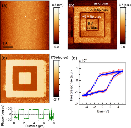
Figures (b)–(c) show typical PFM images (amplitude and phase respectively) for a 17 nm thick c-axis BaTiO3 film grown on SrTiO3 (∼4 nm) on Si substrate, poled with −5 V, +5 V, and −5 V over 6 μm, 4 μm, and 2 μm regions, respectively. Figure (b) indicates similar amplitudes for +P and −P signals with a zero signal at the boundary between opposite poled regions and the graph of figure (c) shows a clear phase difference of ∼180° between +P and −P regions. The as-deposited film (non-poled regions) does not appear mono-domain. A piezoresponse hysteresis loops consistent with ferroelectricity is shown in figure (d). The coercive voltages are of ∼ −1.8 V and +2 V.
Figure 7. (a) Atomic force microscopy topography and piezoresponse force microscopy (b) amplitude and (c) phase images for 17 nm thick BaTiO3/SrTiO3 (∼4 nm) on Si substrate, poled with −5 V, +5 V, and −5 V over 6 μm, 4 μm, and 2 μm regions, respectively. The images were collected over 8 × 8 μm2 areas. The bottom panel in (c) shows the line profile of phase signals, exhibiting clear phase difference of ∼180 degrees. (d) Piezoresponse hysteresis loop averaged over 10 × 10 points within 4 × 4 μm2 area. Error bars represent the dispersion of the signal measured at different locations on the sample surface.
For BaTiO3 grown directly on Ge substrates, no ferroelectricity was reported from electrical or electromechanical measurements with an applied electric field perpendicular to the film, which can be related to the fact that the growth is a-axis oriented [Citation110, Citation116]. In the work by Merckling et al [Citation112] where a mixture of both c-axis tetragonal phase and cubic phase was reported, ferroelectricity was not studied. Ferroelectricity was reported for BaTiO3 c-axis oriented films on (Ba,Sr)TiO3-buffered Ge [Citation115, Citation116]. Current versus voltage curves were measured on capacitive structures with 40 nm BaTiO3 deposited on a trilayer Ba1−xSrxTiO3 buffer (20 nm) stack and with top Pt electrodes, showing rectifying behavior [Citation115]. A hysteresis consistent with ferroelectric switching was observed while no hysteresis was present for a heterojunction with a-axis 60 nm BaTiO3 directly on Ge [Citation115]. In c-axis 16 nm BaTiO3 film on 2 nm SrTiO3 buffered-Ge [Citation116], PFM measurements indicated ferroelectricity with a coercive voltage of −4 V and +5 V. The non-poled regions (as-deposited film) were found to be mono-domain with the polarization oriented towards the STO/Ge substrate, which was in agreement with their theoretical calculations [Citation116]. In addition to the ferroelectricity of BaTiO3, they also demonstrated the ferroelectric field-effect on the conductivity of the underlying Ge using microwave impedance microscopy [Citation116].
Similarly, ferroelectricity in BaTiO3 c-axis film (7.5 nm) on 0.8 nm SrTiO3-GaAs substrate was inferred from PFM measurements, with a repeatedly switchable polarization [Citation128]. Patterns written and read were stable over ∼1 h. The coercive voltage was of the order of ±1–2 V. As-deposited films were poled with a polarization pointing towards the bottom interface [Citation128].
Regarding the dependence of ferroelectricity on the thickness of ultrathin films, very limited work is reported. The thickness dependence in the range 1.6–40 nm of the PFM hysteresis loops was studied in [Citation103] for BaTiO3 on SrTiO3-Si. Films of thickness 40 nm showed closed and saturated hysteresis loops. As the thickness was decreased down to 8 nm, the hysteresis loops were still well-defined with an elongated shape consistent with depolarization field effect [Citation140]. An offset of the electromechanical signal was also observed as thickness decreased [Citation103], which was attributed to imprint phenomenon originating from regions with non- or non-fully-switchable polarization. The coercive voltages for the 16 nm film were of the order of −10 V and +6 V [Citation103], asymmetric and much larger than the ones obtained in the measurement shown in figure for a similar thickness (and for a same SrTiO3 buffer layer thickness of 4 nm). This may be due to the mixed c- and a-domain structure in the study reported in [Citation103] while the film shown in figure is fully c-axis oriented. Fully c-axis oriented films of 8 nm (with a SrTiO3 buffer of 6.2 nm) had coercive voltages of ∼ ±4 V [Citation103].
The ferroelectric polarization of thin and ultrathin films, the coercive field and the ferroelectric domain configuration are strongly dependent on the film thickness as well as on the boundary electrical conditions (nature of the electrodes) and polarization charge screening [Citation141–Citation146]. Garcia et al showed that an ultrathin 1 nm BaTiO3 film epitaxially grown on a metallic manganite electrode is ferroelectric [Citation145]. First-principle computations show that a net positive polarization exists in ultrathin SrTiO3, BaTiO3 or PbTiO3 epitaxial films on silicon but that it cannot be switched as it is pinned by the interface [Citation147]. We recently observed ferroelectricity in ultrathin BaTiO3 films down to 1.6 nm on SrTiO3-buffered silicon [Citation148] but with a strong imprint. For a same film thickness, the thickness of the SrTiO3 buffer layer and the defect chemistry in such layer certainly play a major role in the polarization stability and amplitude in the BaTiO3 film, which is currently under investigation.
Compared to the studies performed on BaTiO3 films grown on oxide substrates (such as SrTiO3 or NdGaO3 bulk crystals), a major difference on growing on semiconductors resides in the strong tensile strain imparted to the film during the cooling time, which may strongly affect the strain state, the defects, the crystalline phase(s) and the crystalline orientation(s) stabilized, which, in turn, impact the ferroelectric properties. Ferroelectric domains in thin BaTiO3 films on silicon and other semiconductors need to be further explored in order to control their size and distribution.
5. Application of BaTiO3 epitaxial films on semiconductors
There are many applications for which ferroelectric epitaxial films on semiconductors can bring new functionalities. As a piezoelectric material, it can be integrated into microelectromechanical systems (MEMS) to design actuators, transducers or sensors [Citation149]. Non-volatile memories have been one of the major application areas of ferroelectrics [Citation150]. Integration of a ferroelectric on silicon offers the ability to fabricate ferroelectric-FETs (FeFETs) as memory or logic devices. We will focus here on two recent areas that have generated several works on the monolithic integration of BaTiO3 on semiconductors. One growing field of interest is in integrated photonics on silicon where building blocks such as electro–optic modulators could benefit from the high Pockels effect of BaTiO3. The other one is in the realization of low power logic devices that has been suggested using the negative capacitance of ferroelectrics.
5.1. Integrated photonics applications
Ferroelectrics are highly attractive for integrated optics to design waveguides with low losses and high bandwidth electro–optic modulators due to their large electro–optic coefficients, optical transparency and thermal stability [Citation151]. In an electro–optic modulator, the phase of the light travelling through the crystal changes depending on the applied electric field. In bulk, lithium niobate LiNbO3 is widely used as an electro–optic medium. Waveguides are designed by modifying the composition of the substrate through diffusion or ion exchange [Citation152] with resulting devices of millimeter or centimeter size. Integrating optical communication functionalities using thin films, especially on silicon platform, stimulates considerable research efforts. Indeed, integration of epitaxial films on silicon offers the ability to co-integrate optical functionalities with standard CMOS ones. Hybrid silicon/lithium niobate optical microring resonators have been recently demonstrated [Citation153–Citation156]. However, the devices on silicon were fabricated from LiNbO3 bonded to silicon using complex techniques. Integrating epitaxial films in a monolithic route would offer much more flexibility. BaTiO3 is particularly attractive for such purpose. It presents high refractive indices (no = 2.412 and ne = 2.36 at 633 nm) with superior linear electro–optic properties compared to LiNbO3, exhibiting one of the highest reported Pockels effect (r113 = 14.5 pm V–1, r33 = 103 pm V–1 and r42 = 1700 pm V–1 at λ = 633 nm from [Citation157]—similar values are also reported in [Citation158]).
Several studies have been conducted on BaTiO3 epitaxially grown on mainly MgO substrates (of lower optical index to allow optical confinement) to design waveguides and electro–optic modulators, either in ridge or strip-loaded configurations and have shown the potential of this material [Citation159, Citation160]. Photonic crystal waveguide structures have been proposed to improve the performance of these devices [Citation161–Citation163]. In a recent work, Li et al showed potential for achieving modulation at 65 GHz [Citation164]. The epitaxial growth of BaTiO3 on SrTiO3 buffered-silicon offers a great potential for performing integrated planar waveguides and electro–optic modulators as well as optical/ferroelectric combined functionalities. Abel et al reported recently for the first time the electro–optical properties of epitaxial BaTiO3 films on SrTiO3/silicon [Citation107]. They showed that BaTiO3 exhibit a much higher effective Pockels coefficient of reff = 148 pm V–1 (λ = 1.55 μm), at least five times larger than the one of LiNbO3. Recently as well, the first monolithically integrated BaTiO3 modulators on SOI substrates were reported [Citation108, Citation165]. Since the silicon has a higher refractive index than BaTiO3, conventional ridge or strip waveguide configurations are not suitable. The design is therefore that of a horizontal slot waveguide in which the a-axis oriented BaTiO3 layer (80 nm) is comprised between the silicon substrate (110 nm Si from the SOI wafer) and an amorphous silicon layer (110 nm) [Citation108]. The waveguide is patterned into the amorphous silicon layer and electrodes are patterned on each side of the waveguide. Mach-Zehnder interferometers and microring resonators were demonstrated [Citation108]. The authors reported an effective Pockels coefficient of reff = 213 ± 49 pm V–1. Similar works pursuing the integration of BaTiO3 on silicon for electro–optic modulators are ongoing [Citation166].
5.2. Low power logic device applications
Power dissipation is one of the major issues that the CMOS nanoelectronic industry is currently facing. For decades, transistor dimensions have been scaled down at constant electric field following Dennard’s rules [Citation167]. Such scaling implied that the supply voltage be reduced and as a consequence, that the threshold voltage Vth of the transistor be reduced, leading after ∼2005 to unacceptable IOFF leakage currents. In order to maintain a high enough ION/IOFF ratio (while the subthreshold swing is thermodynamically limited to 60 mV/dec at room temperature), the scaling rules have therefore been changed to maintain a constant supply voltage. New materials (high-k oxides, III/V semiconductors) and architectures (fully-depleted SOI technology, multiple gate FETs…) have so far allowed us to keep miniaturization compatible with performance although clock frequency has to be limited. The impossibility to further reduce the operating voltage leads to a more general societal issue of energy consumption in a world where individual consumers now posses several electronic products. The percentage of energy consumption by individuals compared to industry keeps growing. There is an urgent need for low-power logic switches that could operate at ∼0.2 V or below and several device concepts have been proposed [Citation168].
In 2008, Salahuddin and Datta suggested that the negative capacitance of a ferroelectric could be used to decrease the subthreshold swing below 60 mV/dec [Citation169]. Although the state of negative capacitance of a ferroelectric is unstable, it could be, however, possible to stabilize it by having in series a suitable positive capacitance. If the ferroelectric is inserted as a gate oxide in a FET and if its thickness is tuned to match the positive one of the silicon/dielectric (interfacial layer e.g.), the two contributions would cancel, leading to a very high effective capacitance. A small change in gate bias could therefore control a large change in the channel charge, meaning low voltage operation [Citation169, Citation170]. There have been many experimental and theoretical works since this initial proposal [Citation171–Citation183]. A sub-60 mV/dec subthreshold swing has been demonstrated in a FET using a ferroelectric polymer [Citation171, Citation177]. A thin AlSi metal was inserted between the ferroelectric layer and the SiO2 interfacial layer, acting as an internal electrode. Slopes ranging from 46 to 58 mV/dec were reported [Citation171]. Several works have focused on combining ferroelectric and paraelectric epitaxial complex oxides in metal–insulator–metal (MIM)-type capacitive structures and demonstrated capacitance enhancement as compared to individual contributions, concluding to negative capacitance effect. Khan et al [Citation174] reported an enhanced capacitance in a bilayer of Pb(Zr0.2Ti0.8)O3/SrTiO3 epitaxially grown on a conducting SrRuO3 electrode at a temperature larger than 500 K. In 2014, two groups have reported room-temperature capacitance enhancement in BaTiO3-based epitaxial heterostructures on SrRuO3. Appleby et al [Citation179] studied BaTiO3/SrTiO3 bilayers and Gao et al [Citation180] studied (LaAlO3/Ba0.2Sr0.8TiO3) superlattices. Recently, Khan et al [Citation181] showed, for the first time, a direct proof for the negative capacitance in an epitaxial Pb(Zr0.2Ti0.8)O3 film on a metallic SrRuO3-buffered SrTiO3 substrate with a top Au electrode. The capacitive structure was put in series with a large resistance in order to be able to measure the transient region when the ferroelectric passes through the unstable negative capacitance state. As a voltage pulse was applied—while a regular capacitor would exhibit an increased voltage—the voltage across the capacitor was shown to decrease, thus indicating a negative capacitance transient [Citation181].
These demonstrations of negative capacitance in MIM structures based on complex ferroelectric oxides give insight into the materials and show that the concept of negative capacitance may hold promise for FET devices. There is, however, no realization so far of a transistor fabricated with a ferroelectric epitaxial oxide on silicon. The reason is the major difficulty to integrate a complex oxide in a transistor following a conventional gate first route. One major issue is the integrity of the ferroelectric after the high-temperature anneal that is required to activate the source and drain regions (typically 1065 °C in the current technologies). A replacement gate route, which experiences a much lower thermal budget, should be followed to save the oxide properties. Another issue is the SiO2 interfacial layer that is formed during BaTiO3 growth on SrTiO3-Si substrates. When as little as few Angström of the low permittivity SiO2 dielectric is formed, it requires the BaTiO3 layer thickness to be increased to few hundreds or few thousands of Angström to reach the capacitance balance. Finally, the concept of negative capacitance FeFET (NC-FeFET) has limitations, which are discussed in details in [Citation178]. One major issue is that the capacitance of the silicon is strongly varying when going from depletion to inversion regimes while the capacitance of the ferroelectric is almost constant in the same voltage range, making the match impossible in the whole operating range. Another concern with using a ferroelectric complex oxide on silicon for NC purpose concerns the charge mismatch: when operating at low voltage, the charge change in Si between OFF and ON states is estimated to ∼0.2 μC cm−2 while the ferroelectric switches much more charges (typically 2–20 μC cm−2) as calculated in [Citation178]. To address these issues, new devices concepts named ‘Quantum metal Fe-FET’ were proposed [Citation178] and are shown in figure . A thin metal layer (called quantum metal) is inserted between the ferroelectric and the semiconductor and is intended to present a constant capacitance to the ferroelectric. It is designed such that its electron carrier density is low and can be modulated by the change in polarization of the ferroelectric layer. For a 2 nm metal layer, the carrier density should be of the order of 1021 cm−3, which could be achieved using doped SrTiO3 [Citation45] or TaNx films [Citation184]. Two different devices were proposed [Citation178]. In one case (device shown in figure (a)), the current flows in the semiconductor inversion layer like in a conventional FET, with the quantum metal’s modulated work function serving as the gate for the semiconductor. In the case of the device in figure (b), the current flows from the quantum metal into the silicon as in a Schottky barrier diode, with the barrier height being modulated by the FE gate electrode. A very steep slope in the channel charge versus gate voltage could be achieved, as shown in figure (c) from the modeling of the device shown in figure (a). The charge changes by 11 orders of magnitude (700 mV change in surface potential) for a 20 mV change in the gate voltage, for a slope of more than 500 decades V–1, or 2 mV/dec for the inverse slope. Hence, such devices are particularly attractive for future low power switches. However, technological challenges to fabricate such devices remain to be addressed.
Figure 8. Device structures for FeFET with quantum metal layer. The arrows indicate current flow paths. (a) With and (b) without a thin insulator between the quantum metal and the semiconductor—(c) calculated Q–V curve for an FeFET as represented in (a)—DOS stands for ‘density of state’. Adapted from figures 4 and 6(a) in [Citation178]. Reprinted with permission of IEEE (D Frank et al 2014 IEEE Trans. Electron Devices 61 2145).
![Figure 8. Device structures for FeFET with quantum metal layer. The arrows indicate current flow paths. (a) With and (b) without a thin insulator between the quantum metal and the semiconductor—(c) calculated Q–V curve for an FeFET as represented in (a)—DOS stands for ‘density of state’. Adapted from figures 4 and 6(a) in [Citation178]. Reprinted with permission of IEEE (D Frank et al 2014 IEEE Trans. Electron Devices 61 2145).](/cms/asset/92bb63d0-e42e-4364-83a8-0c1593e12bcd/tsta_a_11661311_f0008_oc.jpg)
6. Conclusions
We have reviewed studies on epitaxial BaTiO3 grown by MBE on Si, Ge and GaAs semiconducting substrates. The SrTiO3 buffer layer epitaxially grown on these substrates plays a key role to maintain a compressive strain to favor c-axis growth. High crystalline quality and ferroelectric properties were demonstrated on the three substrates. Advancing ferroelectric applications requires better control and understanding of the effect of oxygen and cationic composition on the ferroelectric properties. The domain pattern should be also further investigated in order to control their size and distribution. Engineering of bottom and top interfaces with the ferroelectric layer could offer possible paths to such control. Relatively few works have been done in growing a top metallic electrode in situ in order to possibly control the domain structure. Wetting of Pt on BaTiO3 (as a potential top electrode) has been studied by DFT and experimentally [Citation185]. DFT showed that despite a reasonable match of the lattice constant, the surface energy of both (100) and (110) Pt is too high to wet BaTiO3, which was confirmed by TEM observations, showing Volmer–Weber faceted islands, epitaxial with the underlying BaTiO3 films [Citation185]. Other metals such as TiN or TaN widely used in nanoelectronics should be investigated.
Regarding device fabrication, thick BaTiO3 films show promise in integrated photonics while thin films are of interest for low power logic devices. Heterostructures on Ge, in which no low-permittivity interfacial layer is formed, could be of particular interest to fabricate field-effect transistors with a steep subthreshold swing if the negative capacitance of the ferroelectric could be balanced with the one of the SrTiO3 and Ge contributions. Moreover, the ability to tune the SrTiO3 template to a conducting film using La3+ doping could be used for the design of the quantum metal field-effect transistor.
Progress in the epitaxial growth of perovskite compounds on semiconductors will also open up the route towards more complex heterostructures combining oxide and multiple semiconducting layers. Inserting a ferroelectric or piezoelectric oxide film in a semiconducting quantum well e.g. could enable to modify the electronic and optical properties of the well using ferroelectric field-effect or using piezoelectric strain. It was shown that the properties of a two dimensional electron gas can be modified e.g. by poling of a Cd0.96Zn0.04Te ferroelectric gate deposited on the top of a CdTe-based quantum well structure [Citation186, Citation187] or with a LiNbO3 film on nitride heterostructures [Citation188].
Not addressed here are ferroelectric or piezoelectric/piezotronic nanowires or nanopillars, which are of interest for energy harvesting and sensors applications [Citation189, Citation190]. Other perspectives concern the use of domain walls in the ferroelectric epitaxial films on semiconductors to design specific devices based on new functionalities, not present in the domains [Citation144]. Certain types of domain walls can be conducting while the domains are insulating and the domain walls can be controlled by an electric field [Citation144, Citation191–Citation195]. While works are progressing on ferroelectric/multiferroic perovskites grown on oxide substrates, nothing has been reported, to our knowledge, on silicon. Nanoelectronic based on domain walls would first require the ability to synthesize periodic arrays of domain walls with tunable densities on semiconductors. This area promises exciting future developments.
Acknowledgments
C Magen from Laboratorio de Microscopi´as Avanzadas (LMA), INA-Universidad de Zaragoza, Spain is acknowledged for his contribution to the STEM-HAADF image acquisition. This work was supported by the LABEX iMUST (ANR-10-LABX-0064) of Université de Lyon, within the program ‘Investissements d’Avenir’ (ANR-11-IDEX-0007) operated by the French National Research Agency (ANR). The ANR is also acknowledged for financial support through the program ‘Investissments d’Avenir’ (ANR-10-EQPX-38-01) and support through the grant ANR-14-CE26-0010 (project INTENSE). PFM work was conducted at the Center for Nanophase Materials Sciences, which is a DOE Office of Science User Facility. Support (SMY and SVK) was provided by a DOE Presidential Early Creer Award for Scientists and Engineers. The work (SMY) was also partially supported by IBS-R009-D1.
References
- GlazerA M 1972 The classification of tilted octahedra in perovskites Acta Crystallogr. B 28 3384 10.1107/S0567740872007976
- MannhartJSchlomD G 2010 Oxide interfaces-an opportunity for electronics Science 327 1607 10.1126/science.1181862
- ZubkoPGariglioSGabayMGhosezPTrisconeJ-M 2011 Interface physics in complex oxide heterostructures Annu. Rev. Condens. Matter Phys. 2 141 10.1146/annurev-conmatphys-062910-140445
- HwangH YIwasaYKawasakiMKeimerBNagaosaNTokuraY 2012 Emergent phenomena at oxide interfaces Nat. Mater. 11 103 10.1038/nmat3223
- YuPChuY-HRameshR 2012 Oxide interfaces: pathways to novel phenomena Mater. Today 15 320 10.1016/S1369-7021(12)70137-2
- McKeeR AWalkerF JChisholmM F 1998 Crystalline oxides on silicon: the first five monolayers Phys. Rev. Lett. 81 3014 10.1103/PhysRevLett.81.3014
- ReinerJ WKolpakA MSegalYGarrityK FIsmail-BeigiSAhnC HWalkerF J 2010 Crystalline oxides on silicon Adv. Mater. 22 2919 10.1002/adma.200904306
- ChoA YArthurJ R 1975 Molecular beam epitaxy Prog. Solid State Chem. 10 157 10.1016/0079-6786(75)90005-9
- JoyceB A 1985 Molecular beam epitaxy Rep. Prog. Phys. 48 1637 10.1088/0034-4885/48/12/002
- TheisC DSchlomD G 1996 Cheap and stable titanium source for use in oxide molecular beam epitaxy systems J. Vac. Sci. Technol. A 14 2677 10.1116/1.580185
- JalanBEngel-HerbertRWrightN JStemmerS 2009 Growth of high quality SrTiO3 films using a hybrid molecular beam epitaxy approach J. Vac. Sci. Technol. A 27 461 10.1116/1.3106610
- JalanBMoetakefPStemmerS 2009 Molecular beam epitaxy of SrTiO3 with a growth window Appl. Phys. Lett. 95 032906 10.1063/1.3184767
- DubourdieuC 2005 Pulsed liquid-injection MOCVD of high-K oxides for advanced semiconductor technologies Mater. Sci. Eng. B 118 105 10.1016/j.mseb.2004.12.019
- SchlomD GHarrisJ S Jr 1995 Molecular Beam Epitaxy: Applications to Key Materials FarrowR F C Park Ridge, NJ Noyes p 505
- BozovicIEcksteinJ N 1995 Analysis of growing films of complex oxides by RHEED MRS Bull. 20 32
- HaeniJ HTheisC DSchlomD G 2000 RHEED intensity oscillations for the stoichiometric growth of SrTiO3 thin films by reactive molecular beam epitaxy J. Electroceram. 4 385 10.1023/A:1009947517710
- HaeniJ HTheisC DSchlomD GTianWPanX QChangHTakeuchiIXiangX-D 2001 Epitaxial growth of the first five members of the Srn+1TinO3n+1 Ruddlesden–Popper homologous series Appl. Phys. Lett. 78 3292 10.1063/1.1371788
- NieY F 2014 Atomically precise interfaces from non-stoichiometric deposition Nat. Commun. 5 4530 10.1038/ncomms5530
- CabanelRHirtzJ PEtiennePFruchterLGiovannellaCCreuzetG 1988 On the route to epitaxial growth of YBa2Cu3Oy superconducting thin films by molecular beam epitaxy Physica C 153 407 10.1016/0921-4534(88)90656-9
- YangK YHommaHLeeRBhadraRLocquetJ-PBruynseraedeYSchullerI K 1988 Preparation of high Tc YBCO superconducting thin films by MBE techniques MRS Proc. EA-14 357
- WatanabeSKawaiMHanadaT 1990 Molecular beam epitaxy of Bi2Sr2CuOx using NO2 as an oxidizing agent Japan. J. Appl. Phys. 29 L1111 10.1143/JJAP.29.L1111
- JohnsonB RBeauchampK MWangTLiuJ-XMcGreerK AWanJ CTuominenMZhangY-JMecartneyM LGoldmanA M 1990 In situ growth of DyBa2Cu3O7-x thin films by molecular beam epitaxy Appl. Phys. Lett. 56 1911 10.1063/1.103225
- AchutharamanV SBeauchampK MChandrasehkharNSpaldingG CJohnsonB RGoldmanA M 1992 Fabrication of high-Tc superconductors using ozone-assisted molecular beam epitaxy Thin Solid Films 216 14 10.1016/0040-6090(92)90861-5
- LocquetJ PMachlerE 1992 Characterization of a radio frequency plasma source for molecular beam epitaxial growth of high Tc superconductors films J. Vac. Sci. Technol. A 10 3100 10.1116/1.577871
- BozovicIEcksteinJ NVirshupM FChaikenAWallMHowellRFlussM 1994 Atomic-layer engineering of cuprate superconductors J. Supercond. 7 187 10.1007/BF00730392
- MatijasevicV CBogersSChenN YAppelboomH MHadleyPMooijJ E 1994 Electric-field-induced superconductivity in an overdoped cuprate superconductor Physica C 235 2097 10.1016/0921-4534(94)92269-1
- EcksteinJ NBozovicI 1995 High temperature superconducting multilayers and heterostructures grown by atomic layer-by-layer molecular beam epitaxy Annu. Rev. Mater. Sci. 25 679 10.1146/annurev.ms.25.080195.003335
- YamamotoYNaitoMSatoH 1997 Surface and interface study on MBE-grown Nd1.85Ce0.15CuO4 thin films by photoemission spectroscopy and tunnel spectroscopy Phys. Rev. B 56 2852 10.1103/PhysRevB.56.2852
- NaitoMYamamotoHSatoH 1998 Reflection high-energy electron diffraction and atomic force microscopy studies on homoepitaxial growth of SrTiO3 (001) Physica C 305 233 10.1016/S0921-4534(98)00338-4
- SchlomD GHaeniJ HLettieriJTheisC DTianWJiangJ CPanX Q 2001 Oxide nanoengineering using MBE Mater. Sci. Eng. B 87 282 10.1016/S0921-5107(01)00726-7
- TheisC DYehJSchlomD GHawleyM EBrownG WJiangJ CPanX Q 1998 Adsorption-controlled growth of Bi4Ti3O12 by reactive MBE Appl. Phys. Lett. 72 2817 10.1063/1.121468
- QiaoL 2013 The impacts of cation stoichiometry and substrate surface quality on nucleation, structure, defect formation, and intermixing in complex oxide heteroepitaxy—LaCrO3 on SrTiO3 (001) Adv. Funct. Mater. 23 2953 10.1002/adfm.201202655
- TheisC DSchlomD G 1997 Epitaxial lead titanate grown by MBE J. Cryst. Growth 174 473 10.1016/S0022-0248(96)01144-X
- TheisC DYehJSchlomD GHawleyM EBrownJ W 1998 Adsoprtion-controlled growth of PbTiO3 by reactive molecular beam eptiaxy Thin Solid Films 325 107 10.1016/S0040-6090(98)00507-0
- FompeyrineJSeoJ WLocquetJ P 1999 Growth and characterization of ferroelectric LaTiO3.5 thin films J. Eur. Ceram. Soc. 19 1493 10.1016/S0955-2219(98)00463-4
- SunH PTianWPanX QHaeniJ HSchlomD G 2004 Evolution of dislocation arrays in epitaxial BaTiO3 thin films grown on (100) SrTiO3 Appl. Phys. Lett. 84 3298 10.1063/1.1728300
- GaillardSRozierYMercklingCDucroquetFGendryMHollingerG 2005 LaAlO3 films prepared by MBE on LaAlO3 (001) and Si(001) substrates Microelectron. Eng. 80 146 10.1016/j.mee.2005.04.057
- BarbierAMocutaCStanescuDJegouPJedrecyNMagnanH 2012 Surface composition of BaTiO3/SrTiO3 (100) films grown by atomic oxygen plasma assisted molecular beam epitaxy J. Appl. Phys. 112 114116 10.1063/1.4768469
- MikheevEKajdosA PHauserA JStemmerS 2012 Electric field tunable BaxSr1−xTiO3 films with high figures of merit grown by molecular beam epitaxy Appl. Phys. Lett. 101 252906 10.1063/1.4773034
- NiuGGautierBYinSSaint-GironsGLecoeurPPillardVHollingerGVilquinB 2012 Molecular beam epitaxy growth of BaTiO3 thin films and crucial impact oxygen content conditions on the electrical characteristics Thin Solid Films 520 4595 10.1016/j.tsf.2011.10.182
- IhlefeldJ F 2007 Adsoprtion-controlled molecular-beam epitaxial growth of BiFeO3 Appl. Phys. Lett. 91 071922 10.1063/1.2767771
- SeoJ WFullertonE ENoltingFSchollAFompeyrineJLocquetJ-P 2008 Antiferromagnetic LaFeO3 thin films and their effect on exchange bias J. Phys.: Condens. Matter 20 264014 10.1088/0953-8984/20/26/264014
- JiangJ CPanX QTianWTheisC DSchlomD G 1999 Abrupt PbTiO3/SrTiO3 superlattices grown by reactive molecular beam epitaxy Appl. Phys. Lett. 74 2851 10.1063/1.124035
- MoetakefPOuelletteD GZhangJ YCainT AAllenS JStemmerS 2012 Growth and properties of GdTiO3 films prepared by hybrid molecular beam epitaxy J. Cryst. Growth 355 166 10.1016/j.jcrysgro.2012.06.052
- SonJMoetakefPJalanBBierwagenOWrightN JEngel-HerbertRStemmerS 2010 Epitaxial SrTiO3 films with electron mobilities exceeding 30 000 cm2 V−1 s−1 Nat. Mater. 9 482 10.1038/nmat2750
- DemkovA APosadasASeoHLeeJ KSaiN 2011 Emerging physics of oxide heterostructures Phys. Status Solidi b 248 2076 10.1002/pssb.201147181
- FengJYangFWangZ MYangYGuLZhangJ DGuoJ D 2012 Growth of SrTiO3 (110) film by oxide molecular beam epitaxy with feedback control Appl. Phys. Lett. 2 041407 10.1063/1.4773555
- MoyerJ AEatonCEngel-HerbertR 2013 Highly conductive SrVO3 as a bottom electrode for functional perovskite oxides Adv. Mater. 25 3578 10.1002/adma.201300900
- ScafettaM DXieY JTorresMSpanierJ EMayS J 2013 Optical absorption in epitaxial La1−xSrxFeO3 thin films Appl. Phys. Lett. 102 081904 10.1063/1.4794145
- ZhangK H LSushkoP VColbyRDuYBowdenM EChambersS A 2014 Reversible nano-structuring of SrCrO3-δ through oxidation and reduction at low temperature Nat. Commun. 5 4669 10.1038/ncomms5669
- BaiuttiFChristianiGLogvenovG 2014 Towards precise defect control in layered oxide structures by using oxide molecular beam epitaxy Beilstein J. Nanotechnol. 5 596 10.3762/bjnano.5.70
- RutkowskiM MMcNicholasKZengZ QTuomistoFBrillsonL J 2014 Optical identification of oxygen vacancy formation at SrTiO3-(Ba,Sr)TiO3 heterostructures J. Phys. D: Appl. Phys. 47 255303 10.1088/0022-3727/47/25/255303
- ChoiM 2014 Structural, optical, and electrical properties of strained La-doped SrTiO3 films J. Appl. Phys. 116 043705 10.1063/1.4891225
- YamamotoHKrockenbergerYNaitoM 2014 Augmented methods for growth and development of novel multi-cation oxides Proc. SPIE 8987 89870V
- SeoJ WFompeyrineJGuillerANorgaGMarchioriCSiegwartHLocquetJ P 2003 Interface formation and defect structures in epitaxial La2Zr2O7 thin films on (111)Si Appl. Phys. Lett. 83 5211 10.1063/1.1635966
- MiY YYuZWangS JLimP CFooY LHuanA C HOngC K 2007 Epitaxial LaAlO3 thin film on silicon: structure and electronic properties Appl. Phys. Lett. 90 181925 10.1063/1.2736277
- MercklingC 2007 Epitaxial growth of LaAlO3 on Si(001) using interface engineering Microelectron. Reliab. 47 540 10.1016/j.microrel.2007.01.036
- ReinerJ WPosadasAWangMMaT PAhnC H 2008 Growth and structural properties of crystalline LaAlO3 on Si(001) Microelectron. Eng. 85 36 10.1016/j.mee.2007.07.004
- Sawkar-MathurMMarchioriCFompeyrineJToneyM FBargarJChangJ P 2010 Structural properties of epitaxial SrHfO3 thin films on Si (001) Thin Solid Films 518 S118 10.1016/j.tsf.2009.10.068
- RosselC 2006 Field-effect transistors with SrHfO3 as gate oxide Appl. Phys. Lett. 89 053506 10.1063/1.2236464
- PosadasABergMSeoHde LozanneADemkovA ASmithD JKirkPZhermokletovDWallaceR M 2011 Epitaxial integration of ferromagnetic correlated oxide LaCoO3 with Si(100) Appl. Phys. Lett. 98 053104 10.1063/1.3549301
- ParkJ W 2010 Creation of a two-dimensional electron gas at an oxide interface on silicon Nat. Commun. 1 94 10.1038/ncomms1096
- BaekS-HEomC-B 2013 Epitaxial integration of perovskite-based multifunctional oxides on silicon Acta Mater. 61 2734 10.1016/j.actamat.2012.09.073
- ScigajMDixNFinaIBacheletRWarot-FonroseBFontcubertaJSanchezF 2013 Ultra-flat BaTiO3 epitaxial films on Si(001) with large out-of-plane polarization Appl. Phys. Lett. 102 112905 10.1063/1.4798246
- NgoT GPosadasA BMcDanielM DHuCBruleyJYuE TDemkovA AEkerdtJ G 2014 Epitaxial c-axis oriented BaTiO3 thin films on SrTiO3-buffered Si(001) by atomic layer deposition Appl. Phys. Lett. 104 082910 10.1063/1.4867469
- ColderHDomengesBJorelCMariePBoisserieMGuillonSNicuLGaldiAMéchinL 2014 Structural characterisation of BaTiO3 thin films deposited on SrRuO3/YSZ buffered silicon substrates and silicon microcantilevers J. Appl. Phys. 115 053506 10.1063/1.4863542
- SingamaneniS RPunugupatiSPraterJ THunteFNarayanJ 2014 Ferroelectric and ferromagnetic properties in BaTiO3 thin films on Si(100) J. Appl. Phys. 116 094103 10.1063/1.4894508
- LiZGuoXLuH-BZhangZSongDChengSBosmanMZhuJDongZZhuW 2014 An epitaxial ferroelectric tunnel junction on silicon Adv. Mater. 26 7185 10.1002/adma.201402527
- DubourdieuCGélardISalicioOSaint-GironsGVilquinBHollingerH 2010 Oxides heterostructures for nanoelectronics Int. J. Nanotechnol. 7 2010 10.1504/IJNT.2010.031723
- YuZRamdaniJCurlessJ AOvergaardC DFinderJ MDroopadREisenbeiserK WHallmarkJ AOomsW JKaushikV S 2000 Epitaxial oxide thin films on Si (001) J. Vac. Sci. Technol. B 18 2139 10.1116/1.1303737
- VaithynathanV 2006 c-axis oriented BaTiO3 films on (001) Si J. Appl. Phys. 100 024108 10.1063/1.2203208
- YuZDroopadRRamdaniJCurlessJ AOvergaardC DFinderJ MEisenbeiserK WWangJHallmarkJ AOomsW J 1999 Properties of epitaxial SrTiO3 thin films grown on silicon by molecular beam epitaxy Mater. Res. Soc. Symp. Proc. 567 427 10.1557/PROC-567-427
- EisenbeiserK 2000 Field effect transistors with SrTiO3 gate dielectric on Si Appl. Phys. Lett. 76 1324 10.1063/1.126023
- WeiYHuXLiangYKordanD CCraigoBDroopadRYuZDemkovAEdwardsJ L Jr OomsW J 2002 Mechanism of cleaning Si(100) surface using Sr or SrO for the growth of crystalline SrTiO3 films J. Vac. Sci. Technol. B 20 1402 10.1116/1.1491547
- LiH 2003 Two-dimensional growth of high-quality strontium titanate thin films on Si J. Appl. Phys. 93 4521 10.1063/1.1562001
- ZhangXDemkovA ALi Hao HuXWeiYKulikJ 2003 Atomic and electronic structure of the Si/SrTiO3 interface Phys. Rev. B 68 125323 10.1103/PhysRevB.68.125323
- HuX 2003 The interface of epitaxial SrTiO3 on silicon: in situ and ex situ studies Appl. Phys. Lett. 82 203 10.1063/1.1536247
- JeonSWalkerF JBillmanC AMcKeeR AHwangH 2003 Electrical characteristics of epitaxially grown SrTiO3 on silicon for metal–insulator–semiconductor gate dielectric applications IEEE Electron Dev. Lett. 24 218 10.1109/LED.2003.810886
- FörstC JAshmanC RSchwarzKBlöchlP E 2003 The interface between silicon and a high-k oxide Nature 427 53 10.1038/nature02204
- Aguirre-TostadoF SHerrera-GómezAWoicikJ CDroopadRYuZSchlomD GZschackPKarapetrovaEPianettaPHellbergC S 2004 Elastic anomaly for SrTiO3 thin films grown on Si(001) Phys. Rev. B 70 201403(R) 10.1103/PhysRevB.70.201403
- YuZ 2004 Advances in heteroepitaxy of oxides on silicon Thin Solid Films 462–463 51 10.1016/j.tsf.2004.05.088
- WoicikJ CLiHZschackPKarapetrovaERyanPAshmanC RHellbergC S 2006 Anomalous lattice expansion of coherently strained SrTiO3 thin films grown on Si(001) by kinetically controlled sequential deposition Phys. Rev. B 73 024112 10.1103/PhysRevB.73.024112
- NorgaG JMarchioriCRosselCGuillerALocquetJ-PSiegwartHCaimiDFompeyrineJSeoJ WDiekerC 2006 Solid phase epitaxy of SrTiO3 on (Ba,Sr)O/Si(100): the relationship between oxygen stoichiometry and interface stability J. Appl. Phys. 99 084102 10.1063/1.2190078
- MarchioriCSousaMGuillerASiegwartHLocquetJ-PFompeyrineJNorgaGSeoJ W 2006 Thermal stability of the SrTiO3/(Ba,Sr)O stacks epitaxially grown on Si Appl. Phys. Lett. 88 072913 10.1063/1.2174095
- DelhayeGMercklingCEl-KazziMSaint-GironsGGendryMRobachYHollingerGLargeauLPatriarcheG 2006 Structural properties of epitaxial SrTiO3 thin films grown by molecular beam epitaxy on Si(001) J. Appl. Phys. 100 124109 10.1063/1.2407273
- DelhayeGEl KazziMGendryMHollingerGRobachY 2007 Hetero-epitaxy of SrTiO3 on Si and control of the interface Thin Solid Films 515 6332 10.1016/j.tsf.2006.11.187
- MiS-BJiaC-LVaithyanathanVHoubenLSchubertJSchlomD GUrbanK 2008 Atomic structure of the interface between SrTiO3 thin films and Si(001) substrates Appl. Phys. Lett. 93 101913 10.1063/1.2981524
- ReinerJ WGarrityK FWalkerF JIsmail-BeigiSAhnC H 2008 Role of strontium in oxide epitaxy on silicon (001) Phys. Rev. Lett. 101 105503 10.1103/PhysRevLett.101.105503
- WarusawithanaM P 2009 A ferroelectric oxide made directly on silicon Science 324 367 10.1126/science.1169678
- ParkJ WBaekS HBarkC WBiegalskiM DEomC B 2009 Quasi-single-crystal (001) SrTiO3 templates on Si Appl. Phys. Lett. 95 061902 10.1063/1.3202398
- NiuGSaint-GironsGVilquinBDelhayeGMauriceJ-LBotellaCRobachYHollingerG 2009 Molecular beam epitaxy of SrTiO3 on Si (001): early stages of the growth and strain relaxation Appl. Phys. Lett. 95 062902 10.1063/1.3193548
- WangX FWangJLiQMorenoM SZhouX YDaiJ YWangYTangD 2009 Interfacial structure of epitaxial SrTiO3 on Si: experiments and simulations J. Phys. D: Appl. Phys. 42 085409 10.1088/0022-3727/42/8/085409
- D P KumahD P 2010 The atomic structure and polarization of strained SrTiO3/Si Appl. Phys. Lett. 97 251902 10.1063/1.3529460
- SegalYReinerJ WZhangZAhnC HWalkerF J 2010 Morphology of epitaxial SrTiO3/Si (001) determined using three-dimensional diffraction profile analysis J. Vac. Sci. Technol. B 28 C5B1 10.1116/1.3420394
- NiuGPengW WSaint-GironsGPenuelasJRoyPBrubachJ BMauriceJ LHollingerGVilquinB 2011 Direct epitaxial growth of SrTiO3 on Si (001): interface, crystallization and IR evidence of phase transition Thin Solid Films 519 5722 10.1016/j.tsf.2010.12.208
- ChoiMPosadasADargisRShihC KDemkovA ATriyosoD HTheodoreN DDubourdieuCBruleyJJordan-SweetJ 2012 Strain relaxation in single crystal SrTiO3 grown on Si (001) by molecular beam epitaxy J. Appl. Phys. 111 064112 10.1063/1.3695998
- HellbergC SAndersenK ELiHRyanP JWoicikJ C 2012 Structure of SrTiO3 films on Si Phys. Rev. Lett. 108 166101 10.1103/PhysRevLett.108.166101
- ChoiMPosadasA BSeoHHatchR CDemkovA A 2013 Charge transfer in Sr zintl template on Si(001) Appl. Phys. Lett. 102 031604 10.1063/1.4788916
- SeoHChoiMPosadasA BHatchR CDemkovA A 2013 Combined in situ photoemission spectroscopy and density functional theory of the Sr zintl template for oxide heteroepitaxy on Si(001) J. Vac. Sci. Technol. B 31 04D107-1 10.1116/1.4807716
- ZhangLEngel-HerbertR 2014 Growth of SrTiO3 on Si(001) by hybrid molecular beam epitaxy Phys. Status Solidi RRL 8 917 10.1002/pssr.201409383
- NiuFWesselsB W 2007 Epitaxial growth and strain relaxation of BaTiO3 thin films on SrTiO3 buffered (001) Si by molecular beam epitaxy J. Vac. Sci. Technol. B 25 1053 10.1116/1.2539503
- NiuGYinSSaint-GironsGGautierBLecoeurPPillardVHollingerGVilquinB 2011 Epitaxy of BaTiO3 thin film on Si(001) using a SrTiO3 buffer layer for non-volatile memory application Microelectron. Eng. 88 1232 10.1016/j.mee.2011.03.028
- DubourdieuC 2013 Switching of ferroelectric polarization in epitaxial BaTiO3 films on silicon without a conducting bottom electrode Nat. Nanotechnol. 8 748 10.1038/nnano.2013.192
- AbelSSousaMRosselCCaimiDRossellM DErniRFompeyrineJMarchioriC 2013 Controlling tetragonality and crystalline orientation in BaTiO3 nano-layers grown on Si Nanotechnology 24 285701 10.1088/0957-4484/24/28/285701
- MazetLBacheletRLouahadjLAlbertiniDGautierBCoursRSchamm-ChardonSSaint-GironsGDubourdieuC 2014 Structural study and ferroelectricity of epitaxial BaTiO3 films on silicon grown by molecular beam epitaxy J. Appl. Phys. 116 214102 10.1063/1.4902165
- DroopadRContreras-GuerreroRVeazeyJ PQiaoQKlieR FLevyJ 2013 Epitaxial ferroelectric oxides on semiconductors- a route towards negative capacitance devices Microelectron. Eng. 109 290 10.1016/j.mee.2013.03.124
- AbelS 2013 Strong electro–optically active lead-free ferroelectric integrated on silicon Nat. Commun. 4 1671 10.1038/ncomms2695
- XiongCPerniceW H PNgaiJ HReinerJ WKumahDWalkerF JAhnC HTangH X 2014 Active silicon integrated nanophotonics: ferroelectric BaTiO3 devices Nano Lett. 14 1419 10.1021/nl404513p
- ZhaoTChenFLuHYangGChenZ 2000 Thickness and oxygen pressure dependent structural characteristics of BaTiO3 thin films grown by laser molecular beam epitaxy J. Appl. Phys. 87 7442 10.1063/1.373007
- McKeeR AWalkerF JChisholmM F 2001 Physical structure and inversion charge at a semiconductor interface with a crystalline oxide Science 293 468 10.1126/science.293.5529.468
- LukanovB RReinerJ WWalkerF JAhnC HAltmanE I 2011 Formation of alkaline-earth template layers on Ge(100) for oxide heteroepitaxy: self-organization of ordered islands and trenches Phys. Rev. B 84 075330 10.1103/PhysRevB.84.075330
- MercklingCSaint-GironsGBotellaCHollingerGHeynsMDekosterJCaymaxM 2011 Molecular beam epitaxy growth of BaTiO3 single crystal on Ge-on-Si(001) substrates Appl. Phys. Lett. 98 092901 10.1063/1.3558997
- FredricksonK DPonathPPosadasA BMcCartneyM RAokiTSmithD JDemkovA A 2014 Atomic and electronic structure of the ferroelectric BaTiO3/Ge(001) interface Appl. Phys. Lett. 104 242908 10.1063/1.4883883
- PonathPPosadasA BHatchR CDemkovA A 2013 Preparation of a clean Ge(001) surface using oxygen plasma cleaning J. Vac. Sci. Technol. B 31 031201 10.1116/1.4798390
- NgaiJ HKumahD PAhnC HWalkerF J 2014 Hysteretic electrical transport in BaTiO3/Ba1−xSrxTiO3/Ge heterostructures Appl. Phys. Lett. 104 062905 10.1063/1.4864648
- PonathP 2015 Carrier density modulation in a germanium heterostructure by ferroelectric switching Nat. Commun. 6 6067 10.1038/ncomms7067
- NashimotoKForkD KGeballeT H 1992 Epitaxial growth of MgO on GaAs(001) for growing epitaxial BaTiO3 thin films by pulsed laser deposition Appl. Phys. Lett. 60 1199 10.1063/1.107404
- TarsaE JDe GraefMClarkeD RGossardA CSpeckJ S 1993 Growth and characterization of (111) and (001) oriented MgO films on (001) GaAs J. Appl. Phys. 73 3276 10.1063/1.352975
- RobeyS W 1998 Interfacial reaction effects in the growth of MgO on GaAs (001) by reactive molecular beam epitaxy J. Vac. Sci. Technol. A 16 2423 10.1116/1.581413
- MurphyT EChenDPhillipsJ D 2004 Electronic properties of ferroelectric BaTiO3/MgO capacitors on GaAs Appl. Phys. Lett. 85 3208 10.1063/1.1804237
- LiangYKulikJEschrichT CDroopadRYuZManiarP 2004 Heteroepitaxy of perovskite oxides on GaAs(001) by molecular beam epitaxy Appl. Phys. Lett. 85 1217 10.1063/1.1783016
- LiangYCurlessJMcCreadyD 2005 Band alignment at epitaxial SrTiO3–GaAs (001) heterojunction Appl. Phys. Lett. 86 082905 10.1063/1.1871364
- KlieR FZhuYAltmanE ILiangY 2005 Atomic structure of epitaxial SrTiO3–GaAs (001) heterojunctions Appl. Phys. Lett. 87 143106 10.1063/1.2077837
- WuZ PHuangWWongK HHaoJ H 2008 Structural and dielectric properties of epitaxial SrTiO3 films grown directly on GaAs substrates by laser molecular beam epitaxy J. Appl. Phys. 104 054103 10.1063/1.2974796
- LouahadjLBacheletRRegrenyPLargeauLDubourdieuCSaint-GironsG 2014 Molecular beam epitaxy of SrTiO3 on GaAs(001): GaAs surface treatment and structural characterization of the oxide layer Thin Solid Films 563 2 10.1016/j.tsf.2014.02.062
- LouahadjL 2013 Ferroelectric Pb(Zr,Ti)O3 epitaxial layers on GaAs Appl. Phys. Lett. 103 212901 10.1063/1.4831738
- Contreras-GuerreroREdirisooriyaMNoriegaO CDroopadR 2013 Interface properties of MBE grown epitaxial oxides on GaAs J. Cryst. Growth 378 238 10.1016/j.jcrysgro.2012.12.131
- Contreras-GuerreroRVeazeyJ PLevyJDroopadR 2013 Properties of epitaxial BaTiO3 deposited on GaAs Appl. Phys. Lett. 102 012907 10.1063/1.4773988
- HuangWWuZ PHaoJ H 2009 Electical properties of ferroelectric BaTiO3 thin film on SrTiO3-buffered GaAs by laser molecular beam epitaxy Appl. Phys. Lett. 94 032905 10.1063/1.3075955
- YangZHaoJ 2012 In-plane dielectric properties of epitaxial Ba0.7Sr0.3TiO3 thin films grown on GaAs for tunable device application J. Appl. Phys. 112 054110 10.1063/1.4749270
- BatraI PWurfelPSilvermanB D 1973 Phase transition, stability, and depolarization field in ferroelectric thin films Phys. Rev. B 8 3257 10.1103/PhysRevB.8.3257
- MillerS LMcWhorterP J 1992 Physics of the ferroelectric nonvolatile memory field-effect transistor J. Appl. Phys. 72 5999 10.1063/1.351910
- GruvermanAKholkinA 2006 Nanoscale ferroelectrics: processing, characterization and future trends Rep. Prog. Phys. 69 2443 10.1088/0034-4885/69/8/R04
- KalininS VRarAJesseS A 2006 decade of piezoresponse force microscopy: progress, challenges, and opportunities IEEE Trans. Ultrason. Ferroelectr. Freq. Control 53 2226 2252 2226–52 10.1109/TUFFC.2006.169
- BalkeNBdikinIKalininS VKholkinA L 2009 Electromechanical imaging and spectroscopy of ferroelectric and piezoelectric materials: state of the art and prospects for the future J. Am. Ceram. Soc. 92 1629 1647 1629–47 10.1111/j.1551-2916.2009.03240.x
- KalininS VJesseSTselevABaddorfA PBalkeN 2011 The role of electrochemical phenomena in scanning probe microscopy of ferroelectric thin films ACS Nano 5 5683 10.1021/nn2013518
- MarshallM S JKumahD PReinerJ WBaddorfA PAhnC HWalkerF J 2012 Piezoelectric force microscopy of crystalline oxide-semiconductor heterostructures Appl. Phys. Lett. 101 102902 10.1063/1.4750243
- BarkC W 2012 Switchable Induced Polarization in LaAlO3/SrTiO3 Heterostructures Nano Lett. 12 1765 10.1021/nl3001088
- KimYMorozovskaA NKumarAJesseSEliseevE AAlibartFStrukovDKalininS V 2012 Ionically-mediated electromechanical hysteresis in transition metal oxides ACS Nano 6 7026 10.1021/nn3020757
- BratkovskyA MLevanyukA P 2006 Depolarizing field and ‘real’ hysteresis loops in nanometer-scale ferroelectric films Appl. Phys. Lett. 89 253108 10.1063/1.2408650
- JunqueraJGhosezP 2003 Critical thickness for ferroelectricity in perovskite ultrathin films Nature 422 506 10.1038/nature01501
- DawberMRabeK MScottJ F 2005 Physics of thin-film ferroelectric oxides Rev. Mod. Phys. 77 1083 10.1103/RevModPhys.77.1083
- SaiNKolpakMRappeA M 2005 Ferroelectricity in ultrathin perovskite films Phys. Rev. B 72 020101 (R) 10.1103/PhysRevB.72.020101
- CatalanGSeidelJRameshR 2012 Domain wall nanoelectronics Rev. Mod. Phys. 84 119 10.1103/RevModPhys.84.119
- GarciaVFusilSBouzehouaneKEnouz-VedrenneSMathurN DBarthélémyABibesM 2009 Giant tunnel electroresistance for non-destructive readout of ferroelectric states Nature 460 81 10.1038/nature08128
- LichtensteigerCFernandez-PenaSWeymannCZubkoPTrisconeJ-M 2014 Tuning of the depolarization field and nanodomain structure in ferroelectric thin films Nano Lett. 14 4205 10.1021/nl404734z
- KolpakA M 2010 Interface-induced polarization and inhibition of ferroelectricity in epitaxial SrTiO3/Si Phys. Rev. Lett. 105 217601 10.1103/PhysRevLett.105.217601
- MazetL 2014 Monolithic integration of epitaxial BaTiO3 on Si and SiGe for ferroelectric devices 61st AVS Baltimore, MD, 9–14 November
- BaekS H 2011 Giant piezoelectricity on Si for hyperactive MEMS Science 334 958 10.1126/science.1207186
- ScottJ F 2000 Ferroelectric Memories Berlin Springer chapter 2.12
- WesselsB W 2007 Ferroeletric epitaxial thin films for integrated optics Annu. Rev. Mater. 37 659 10.1146/annurev.matsci.37.052506.084226
- BaldiPDe MicheliMTanziliJ SOstrowskyD B 2005 Waveguide nonlinear-optic devices and application to quantum information 2005 Pacific Rim Conf. on Lasers and Electro-Optics (Tokyo, 11–15 July 2005) 96 97 p 96–7
- LeeY SKimG-DKimW-JLeeS-SLeeW-GSteierW H 2011 Hybrid Si-LiNbO3 microring electro–optically tunable resonators for active photonic devices Opt. Lett. 36 1119 1121 1119–21 10.1364/OL.36.001119
- ChenLReanoR M 2012 Compact electric field sensors based on indirect bonding of lithium niobate to silicon microrings Opt. Express 20 4032 4038 4032–8 10.1364/OE.20.004032
- ChenLWoodM GReanoR M 2013 12.5 pm–1 hybrid silicon and lithium niobate optical microring resonator with integrated electrodes Opt. Express 21 27003 10.1364/OE.21.027003
- ChenLXuQWoodGReanoR M 2014 Hybrid silicon and lithium niobate electro–optical ring modulator Optica 1 112 118 112–8 10.1364/OPTICA.1.000112
- GodefroyG 1996 Ferroélectricité Tech. de l’Ingénieur E1–870 1
- ZgonikMBernasconiPDuelliMSchlesserRGünterPGarrettM HRytzDZhuYWuX 1994 Dielectric, elastic, piezoelectric, electro–optic, and elasto-optic tensors of crystals Phys. Rev. B 50 5941 10.1103/PhysRevB.50.5941
- GillD MConradC WFordGWesselsB WHoS T 1997 Thin-film channel waveguide electro–optic modulator in epitaxial BaTiO3 Appl. Phys. Lett. 71 1783 10.1063/1.119397
- TangPTownerD JMeierA LWesslesB W 2004 Low-loss electrooptic BaTiO3 thin film waveguide modulator IEEE Photon. Technol. Lett. 16 1837 10.1109/LPT.2004.831255
- LiuZLinP-TWesselsB WYiFHoS-T 2007 Nonlinear photonic crystal waveguide structures based on barium titanate sthin films and their optical properties Appl. Phys. Lett. 90 201104 10.1063/1.2739083
- LinP TYiFHoS-TWesselsB W 2009 Two-dimensional ferroelectric photnonic crystal waveguides: simulation, fabrication and optical characterization J. Lightwave Technol. 27 4330 10.1109/JLT.2009.2023808
- LiJLiuZWesselsB WTuYHoS-TJoshi-ImreAOcolaL E 2011 Hexagonal photonic crystal wave guide based on barium titanate thin films Proc. SPIE 7934 79340R-1
- LiJLiuZTuYHoS-TJungI WOcolaL EWesselsB W 2013 Photonic crystal waveguide electro–optic modulator with a wide bandwidth J. Lightwave Technol. 31 1601 10.1109/JLT.2013.2255025
- PerniceW H PXiongCWalkerF JTangH X 2014 Design of a silicon integrated electro–optic modulator using ferroelectric BaTiO3 films IEEE Photon. Technol. Lett. 26 1344 10.1109/LPT.2014.2322501
- European project FP7-ICT-2013-11-619456: Silicon CMOS compatible transition metal oxide technology for boosting highly integrated photonic devices with disruptive performance (SITOGA) (http://sitoga.eu)
- DennardR HGaensslenF HRideoutV LBassousELeBlancA R 1974 Design of ion-implanted MOSFET’s with very small physical dimensions IEEE J. Solid-State Circuits 9 256 10.1109/JSSC.1974.1050511
- TheisT NSolomonP M 2010 In quest of the ‘next switch’: prospects for greatly reduced power dissipation in a successor to the silicon field-effect transistor Proc. IEEE 98 2005 10.1109/JPROC.2010.2066531
- SalahuddinSDattaS 2008 Use of negative capacitance to provide voltage amplification for low power nanoscale devices Nano Lett. 8 405 10.1021/nl071804g
- ZhirnovV VCavinR K 2008 Negative capacitance to the rescue? Nat. Nanotechnol. 3 77 10.1038/nnano.2008.18
- RusuASalvatoreG AJimenezDIonescuA M 2010 Metal-ferroelectric-metal-oxide-semiconductor field effect transistor with sub-60 mV/decade subthreshold swing and internal voltage amplification Proc. IEDM 16.3.1 16.3.4 p 1–16
- JimenezDMirandaEGodoyA 2010 Analytic model for the surface potential and drain current in negative capacitance field-effect transistors IEEE Trans. Electron Devices 57 2405 10.1109/TED.2010.2062188
- CanoAJimenezD 2010 Multidomain ferroelectricity as a limiting factor for voltage amplification in ferroelectric field-effect transistors Appl. Phys. Lett. 97 133509 10.1063/1.3494533
- KhanA IBhowmikDYuPKimS JPanXRameshRSalahuddinS 2011 Experimental evidence of ferroelectric negative capacitance in nanoscale heterostructures Appl. Phys. Lett. 99 113501 10.1063/1.3634072
- KhanA IYeungC WHuCSalahuddinS 2011 Ferroelectric negative capacitance MOSFET: capacitance tuning & antiferroelectric operation IEEE Int. Electron Devices Meet. p 255
- YeungC WKhanA IChengJ-YSalahuddinSHuC 2012 Non-hysteretic negative capacitance FET with Sub-30 mV/dec swing over 106X current range and ION of 0.3 mA/μm without strain enhancement at 0.3 V VDD SISPAD: Int. Conf. Simul. Semicond. Processes Devices p 257
- SalvatoreG ARusuAIonescuA M 2012 Experimental confirmation of temperature dependent negative capacitance in ferroelectric field effect transistor Appl. Phys. Lett. 100 163504 10.1063/1.4704179
- FrankD JSolomonP MDubourdieuCFrankM MNarayananVTheisT N 2014 The quantum metal ferroelectric field-effect transistor IEEE Trans. Electron Devices 61 2145 10.1109/TED.2014.2314652
- ApplebyD J RPononN KKwaK S KZouBPetrovP KWangTAlfordN MO’NeillA 2014 Experimental observation of negative capacitance in ferroelectrics at room temperature Nano Lett. 14 3864 10.1021/nl5017255
- GaoWKhanAMartiXNelsonCSerraoCRavichandranJRameshRSalahuddinS 2014 Room-temperature negative capacitance in a ferroelectric-dielectric superlattice heterostructure Nano Lett. 14 5814 10.1021/nl502691u
- KhanA IChatterjeeKWangBDrapchoSYouLSerraoCBakaulS RRameshRSalahuddinS 2014 Negative capacitance in a ferroelectric capacitor Nat. Mater. 14 182 10.1038/nmat4148
- JainAAlamM A 2014 Stability constraints define the minimum subthreshold swing of a negative capacitance field-effect transistor IEEE Trans. Electron Devices 61 2235 10.1109/TED.2014.2316167
- JainAAlamM A 2014 Proposal of hysteresis-free zero subthreshold swing field-effect transistor IEEE Trans. Electron Devices 61 3546 10.1109/TED.2014.2347968
- ChoiMDubourdieuCKellockALeeK LHaightR APyzynaAFrankM MDemkovA ANarayananV 2014 Tunable electrical properties of TaNx thin films grown by ionized physical vapor deposition J. Vac. Sci. Technol. B 32 051202 10.1116/1.4891108
- FredricksonK DPosadasA BDemkovA ADubourdieuCBruleyJ 2013 Wetting at the BaTiO3/Pt interface J. Appl. Phys. 113 184102 10.1063/1.4803705
- KolkovskyVWojciechowskiTWojtowiczTG KarczewskiG 2008 Ferroelectric field effect transistor based on modulation doped CdTe/CdMgTe quantum wells Acta Phys. Pol. A 114 1173
- StolichnovICollaESetterNWojciechowskiTJanikEKarczewskiG 2007 Quantum well ZnCdTe/CdTe structures with integrated ferroelectric gates, applications of ferroelectrics ISAF 2007: 16th Int. Symp. on Applications of Ferroelectrics p 52
- SinghMWuY RSinghJ 2003 Examination of LiNbO3/nitride heterostructures Solid State Electron. 47 2155 10.1016/S0038-1101(03)00189-8
- KokaASodanoH A 2013 High-sensitivity accelerometer composed of ultra-long vertically aligned barium titanate nanowire arrays Nat. Commun. 4 2682 10.1038/ncomms3682
- KokaAZhouZSodanoH A 2014 Vertically aligned BaTiO3 nanowire arrays for energy harvesting Energy Environ. Sci. 7 288 10.1039/C3EE42540A
- SeidelJ 2009 Conduction at domain walls in oxide multiferroics Nat. Mater. 8 229 10.1038/nmat2373
- FarokhipoorSNohedaB 2011 Conduction through 71° domain walls in BiFeO3 thin films Phys. Rev. Lett. 107 127601 10.1103/PhysRevLett.107.127601
- VasudevanR KMorozovskaA NEliseevE ABritsonJYangJ CChuY HMaksymovychPChenL QNagarajanVKalininS V 2012 Domain wall geometry controls conduction in ferroelectrics Nano Lett. 12 5524 10.1021/nl302382k
- FeiglLYudinPStolichnovISlukaTShapovalovKMtebwaMSanduC SWeiX-KTagantsevA KSetterN 2014 Controlled stripes of ultrafine ferroelectric domains Nat. Commun. 5 4677 10.1038/ncomms5677
- McGillyL JYudinPFeiglLTagantsevA KSetterN 2015 Controlling domain wall motion in ferroelectric thin films Nat. Nanotechnol. 10 145 10.1038/nnano.2014.320