Abstract
The fabrication, characterization, and decoration with metallic nanoparticles of nanostructures such as nanowhiskers, nanodendrites, and fractal-like nanotrees on insulator substrates by electron-beam-induced deposition (EBID) are reviewed. Nanostructures with different morphologies of whiskers, dendrites, or trees are fabricated on insulator (Al2O3 or SiO2) substrates by EBID in transmission electron microscopes by controlling the irradiation conditions such as the electron beam intensity. The growth of the nanostructure is related to the accumulation of charges on the surface of a substrate during electron-beam irradiation. A high concentration of the target metallic element and nanocrystal grains of the element are contained in the fabricated nanostructures. The process of growth of the nanostructures is explained qualitatively on the basis of mechanisms in which the formation of the nanostructures is considered to be related to the nanoscaled unevenness of the charge distribution on the surface of the substrate, the movement of the charges to the convex surface of the substrate, and the accumulation of charges at the tip of the grown nanostructure. Novel composite structures of Pt nanoparticle/tungsten (W) nanodendrite or Au nanoparticle/W nanodendrite are fabricated by the decoration of W nanodendrites with metallic elements. Because they have superior features, such as a large specific surface area, a freestanding structure on substrates, a typical size of several nanometers of the tip or the branch, and high purity, the nanostructures may have applications in technologies such as catalysts, sensors, and electron emitters. However, there are still some subjects that should be further studied before their application.
Introduction
The fabrication of nanomaterials has attracted much attention in recent years due to their potential applications in the development of functional materials and nanodevices. Significant effort has been made to control the size and morphology of nanostructures, because these parameters primarily determine their properties, such as the electrical and optical properties [Citation1]. Methods for fabricating nanomaterials include chemical vapor decomposition [Citation2], the arc-discharge method [Citation3], evaporation [Citation4], and hydrothermal reactions [Citation5]. Among the methods, electron- and ion-beam-induced deposition (EBID and IBID) have attracted great attention. In these methods, the precursor molecules containing target elements are introduced near a substrate. They are adsorbed on the substrate and are then decomposed by an energetic electron- or ion-beam in a vacuum chamber. The volatile part of the precursor is pumped out while the nonvolatile part containing the target elements remains as a deposit. EBID may be divided into two categories. One is conventional EBID, in which conductive substrates are generally used. A conductive substrate provides stable fabrication conditions. Because of the controllability of the beam and the large number of choices for the precursor, zero, one, two, or three-dimensional small objects have been fabricated [Citation6–14]. The size of the fabricated objects is limited by that of the electron beam, although the objects are usually larger than the size of the electron beam [Citation12, Citation14]. The other category is EBID using insulator substrates. The accumulation of charges readily occurs on an insulator substrate during EBID. The deposition of novel structures may occur under this condition. The growth of carbon fractal-like structures has been observed on insulator substrates under electron-beam (EB) irradiation due to the existence of residual pump oil in the atmosphere of the vacuum chamber [Citation15–17], but the intentional performance of EBID using insulator substrates was first reported recently [Citation18]. By using insulator substrates such as Al2O3 and SiO2, characteristic morphologies of nanostructures, such as arrays of nanowhiskers (or nanowires), arrays of nanodendrites, and fractal treelike structures, have been fabricated in transmission electron microscopes (TEMs) by EBID [Citation18–23]. The typical size of the diameter of a nanowhisker, the tip of a nanodendrite, and the tip of a nanotree is about 3 nm, and is almost completely independent of the size of the EB. The successful fabrication of these nanostructures by EBID suggests a new method of fabricating novel nanostructures, such as the composite structure of Pt nanoparticle/tungsten (W) nanodendrite or Au nanoparticle/W nanodendrite [Citation24]. In this paper we review the fabrication, characterization, and decoration with metallic nanoparticles of nanostructures fabricated on insulator substrates by EBID, and discuss the possible applications and problems to be solved in the future.
EBID experiment
EBID was performed using JEM-2010 or JEM-ARM1000 TEMs made by JEOL Co., Ltd. The energy of the EB was from 200 to 1000 keV. The pressure in the specimen chambers of the TEMs was on the order of 10−5 to 10−6 Pa. Insulators suitable for observation using a TEM were used as the substrates. An organometallic precursor gas was introduced near the substrate using a special designed system comprising a nozzle with a diameter smaller than 0.1 mm and a reservoir containing the precursor [Citation18]. Hexacarbonyl (W(CO)6) or C5H5Pt(CH3)3 was used as the precursor for fabricating tungsten (W)-containing, or platinum (Pt)-containing nanostructures, respectively. The vapor pressures of these precursors are several Pa at room temperature. These precursors have been previously typically used to fabricate small objects on conductive substrates by EBID [Citation7]. The intensity of the EB for the EBID was from 3.2 to 111.7×10¹⁸ e cm−2 s−1 (current density: 0.51 to 17.9 A cm−2), which was estimated by measuring the total intensity and the size of the EB under operating conditions. The fabricated structure was characterized in situ or after fabrication in a TEM. The experiments were performed at room temperature.
Morphology of tungsten nanostructures
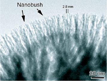
By EBID on insulator substrates, nanostructures can be fabricated that are different from the compact deposits fabricated using conductive substrates. Figure shows a micrograph of an array of W nanowhiskers (or nanowires) fabricated on an Al2O3 substrate irradiated with a 200 keV EB at an intensity of 4.7×10¹⁸ e cm−2 s−1 (0.75 A cm−2) for about 120 s [Citation18]. The nanowhiskers grew in a narrow area near the edge of the substrate within the EB-irradiated area. They were freestanding and grew normal to the surface of the substrate and were separated from each other by several nanometers. The thickness of these whiskers is about 3 nm. EBID by elongated irradiation with an EB results in the morphology of a nanobush, as shown in figure [Citation19]. Another experiment was carried out to fabricate W nanowhiskers on SiO2 substrates by EBID using a 400 keV EB at an intensity of 5.2×10¹⁸ e cm−2 s−1 (0.83 A cm−2) [Citation20]. The nucleation and growth of the nanowhiskers were investigated. It was revealed that nanodots of 2 to 3 nm in size were formed on the surface of the substrate and then nanowhiskers grew from the nanodots. A size of 2 to 3 nm seemed to be the threshold size for a nanodot to grow to a nanowhisker. It was also observed that the nanowhiskers grew from their tips, and that the growth rate depended on the local conditions of the substrate.
Figure 1 W nanowhisker arrays fabricated on the surface of an Al2O3 substrate by EBID. The intensity of the EB was 4.7×10¹⁸ e cm−2 s−1 (0.75 A cm−2) and the irradiation time was 120 s. (Reproduced with permission from [Citation18], © 2005, Springer Science+Business Media.)
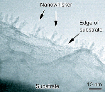
Figure 2 W nanobushs fabricated on the surface of an Al2O3 substrate by EBID. The intensity of the EB was 4.7×10¹⁸ e cm−2 s−1 (0.75 A cm−2) and the irradiation time was 19 min. (Reproduced with permission from [Citation19], © 2005, Blackwell.)
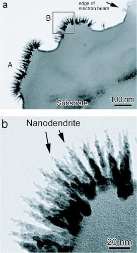
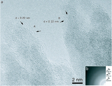
Irradiation with a more intense EB results in the growth of nanodendrites [Citation18]. Figure shows micrographs of an array of nanodendrites fabricated on an Al2O3 substrate using an EB with an intensity of 2.0×10¹⁹ e cm−2 s−1 (3.2 A cm−2) for 30 s. The edge of the EB is indicated in figure (a). The contrast inside the irradiated area is darker than that outside the irradiated area because a compact layer was deposited within the irradiated area. However, the nanodendrites grew almost exclusively on convex surface, as shown by A and B in figure (a), indicating that the conditions required for nanodendrites are different from those required for nanowhiskers. The typical thickness of the tip of a nanodendrite is about 3 nm. Note that the EB was defocused and had almost an even current density over the entire irradiated area [Citation25]. Arrays of nanodendrites were also successfully fabricated on SiO2 substrates by EBID when the energy of the EB was from 400 to 1000 keV [Citation21–23]. The length of nanodendrites increased approximately linearly with the electron fluence [Citation21].
Figure 3 Arrays of W nanodendrites fabricated on the surface of an Al2O3 substrate by EBID. The intensity of the EB was 2.0×10¹⁹ e cm−2 s−1 (3.2 A cm−2) and the irradiation time was 30 s (a) A micrograph showing that the nanodendrites only grow on the convex surfaces indicated by A and B, (b) an enlargement of part of (a), showing the detail of the nanodendrites. (Reproduced with permission from [Citation18], © 2005, Springer Science+Business Media.)
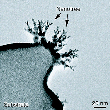
As the intensity of the EB used in EBID is increased further, fractal-like W nanotrees are fabricated. An example is shown in figure [Citation18]. The intensity of the EB was 1.1×10²⁰ e cm−2 s−1 (17.9 A cm−2) and the irradiation time was 10 s. Many branches with a thickness of about 3 nm were formed.
Figure 4 Fractal-like W nanotrees fabricated on the surface of an Al2O3 substrate by EBID. The intensity of the EB was 1.1×10²⁰ e cm−2 s−1 (17.9 A cm−2) and the irradiation time was 10 s. (Reproduced with permission from [Citation18], © 2005, Springer Science+Business Media.)
The nanowhisker, nanobush, nanodendrite, and nanotree are very characteristic structures because they have never been observed to grow on conductive substrates and only grow on insulator substrates by EBID or IBID. Table 1 summarizes the typical conditions for the growth of the different W nanostructures on Al2O3 substrates by EBID using a 200 keV EB [Citation18]. It is clear that different morphologies can be fabricated by controlling the intensity of the EB.
Typical conditions for the growth of W nanostructures on Al2O3 substrates by EBID using a 200 keV EB.
Dependence of the growth on accumulation of charges on surface
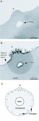
Since the nanostructures discussed in the previous section only grow on insulator substrates, the accumulation of charges on the insulator substrate during EB irradiation may be closely related to their growth. To confirm this supposition, a sample with a hole and a convex surface was selected for the growth of nanodendrites [Citation26]. Figure (a) shows the area before the EBID was performed. A hole of about 40 nm diameter and a convex surface indicated by A can be observed. An EB with an intensity of 3.1×10¹⁹ e cm−2 s−1 (5.0 A cm−2) was applied and maintained for 10 s. The area was then imaged as shown in figure (b). The size of the EB is identified by the dark contrast in the figure, which originates from the compact layer deposited in the EB-irradiated area. Nanodendrites grew only on the convex surface and not on the edge of the hole. However, a compact layer was deposited on the edge of the hole causing the diameter of the hole to decrease to about 25 nm. These results can be understood by considering the difference in the charge distribution between the convex surface and the edge of the hole during the EB irradiation. It is known that a compact W deposit is conductive [Citation6, Citation8]. Since the deposited W layer with dark contrast shown in figure (b) was formed in the EB-irradiated area, the irradiated area can be considered to be a conductive ring. The distribution of charges is schematically shown in figure (c) on the basis of a simple consideration of a conductor ring charged with static electricity. The charges should not be distributed in the inner surface of the ring (here, the surface of the hole) but on the outer surface of the ring. The nanodendrites grew only on the outer convex surface of the substrate, providing evidence that the growth of the nanodendrites is related to the accumulation of charges. On the other hand, there is no accumulation of charges on the inner surface of the hole; therefore, a compact deposit is formed on the surface, which is similar to the case of EBID on a conductive substrate.
Figure 5 W nanodendrites fabricated by EBID on a sample with a hole and a convex surface. (a) The micrograph of the area before EBID; (b) the micrograph of the area after EBID. The intensity of the EB was 3.1×10¹⁹ e cm−2 s−1 (5.0 A cm−2) and the irradiation time was 10 s; (c) a schematic drawing of the charge distribution during EBID in the EB-irradiated area. (Reproduced with permission from [Citation26], © 2005, Elsevier.)
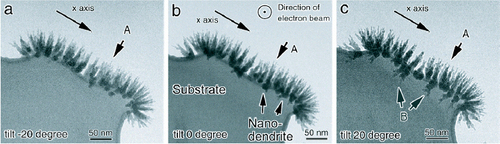
Another observation provides convincing evidence that the growth of nanodendrites is related to the electric field generated by the accumulated charges on the convex surface [Citation25]. Figure shows micrographs of nanodendrites fabricated on an Al2O3 substrate by EBID. The nanodendrites are fabricated on the substrate when it is not tilted. After the fabrication, the substrate is tilted and the nanodendrites are observed. The EB was irradiated from vertically above the plane of the figure, as indicated in figure (b). The positive rotation of the x-axis is clockwise when looking from the end to the tip of the x-axis arrow. The lengths of the nanodendrites on the plane shown in the figures near the place indicated by arrow A were measured as 64, 60 and 55 nm for the three angles of tilt in figures (a)–(c), respectively. The difference in length was small, which revealed that the nanodendrites grew radially and at almost the same speed from the surface of the substrate over a wide solid angle. The small difference in length may be attributed to the trajectory effects of the incident EB, such as sputtering and moving atoms to the incident direction, since the dendrites are longer in the incident EB direction than in the reverse direction. Some nanodendrites can be observed in figure (c), as shown by arrow B, but cannot be observed clearly in figure (b). It is considered that these nanodendrites grew from the substrate in the direction almost parallel to that of the incident EB during the EBID. Since the gradient of the electric field generated by accumulated charges at the edge of the substrate is normal to the surface, it is clear that the nanodendrites grew parallel to the gradient of the electric field.
Figure 6 W nanodendrites fabricated on an Al2O3 substrate by EBID observed with different tilting angles of the substrate; (a), (b) and (c) are micrographs with the substrate tilted at −20°, 0° and 20°, respectively. The EBID is performed when the substrate is untilted.
Growth mechanisms of the nanostructures
Precursor molecules are adsorbed on the surface of a substrate and are decomposed or dissociated by the EB during EBID. The dissociation cross section, which indicates the probability of the dissociation or decomposition of a molecule by an electron, depends on the electron energy. The dissociation cross sections are known for simple gases, such as N2, CH4 and CF4 [Citation27], but there is limited data for gases used in EBID [Citation28, Citation29]. Generally, a dissociation cross-section curve has a peak at a low energy of approximately 100 eV. Thus, low-energy electrons, such as secondary electrons, play an important role in EBID. The secondary electron distribution from an EB-irradiated substrate has been studied using a Monte Carlo method [Citation30–32].
However, for an insulator substrate, in addition to the production and distribution of the secondary electrons, the accumulation of charges on the irradiated surface is related to the growth of the deposit during EBID. The details of the relationship have not yet been clarified. Qualitative mechanisms have been proposed for the growth of W nanostructures in a different morphology on an insulator substrate based on suppositions about the distribution and movement of the charges on the surface of a substrate [Citation18]. It was concluded that three factors were involved in the growth of the observed structures, namely, the nanometer-scale uneven distribution of the charges on the substrate, the movement of the charges to a convex surface or to the tip of the deposit, and the accumulation of the charges at the tip of the deposit.
Figure shows the mechanisms schematically [Citation18]. In figure (a), the growth mechanism of a nanowhisker array is shown. The intensity of the EB is weak, but the accumulation of charges occurs. The distribution of the charges on the surface is assumed to be uneven at a nanometer scale. Charges may accumulate at some places (charge centers), where an electric field is generated. The dark dots represent the nonvolatile fraction of the precursor molecules of which the deposits are composed, while the brighter dots represent the volatile fraction. Because the intensity of the EB is weak, the adsorbed molecules can move around considerably before being decomposed. The precursor molecules adsorbed on the surface may be attracted to the charge centers since the molecules are easily polarized due to the weak bonding between the atoms of the molecules. The precursor molecules then decompose and form a deposit. After a deposit is formed, the charges on the surface of the substrate or the deposit tend to move and accumulate at the tip of the deposit, since W deposits have been reported to be conductive [Citation6, Citation8]. Thus, molecules are attracted to the tip, and the deposit increases in length upon further EB irradiation. The formation of W nanodot deposits on the surface of a SiO2 substrate and the growth of W nanowhiskers from these nanodots [Citation20] are consistent with the above mechanism. The growth of a nanobush can also be understood qualitatively on the basis of the above mechanism [Citation19].
Figure 7 Schematic drawings showing the process of growth of nanostructures with different morphologies on insulator substrates by EBID. The dark dots represent the nonvolatile fraction of the precursor and the deposit, while the brighter dots represent the volatile fraction of the precursor. (a) The growth of nanowhiskers (or nanowires) inside the area of irradiation with a weak EB; (b) the growth of nanodendrites on a convex surface under irradiation with a moderate EB; and (c) the growth of fractal-like nanotrees on a convex surface under irradiation with a strong EB. (Reproduced with permission from [Citation18], © 2005, Springer Science+Business Media.)
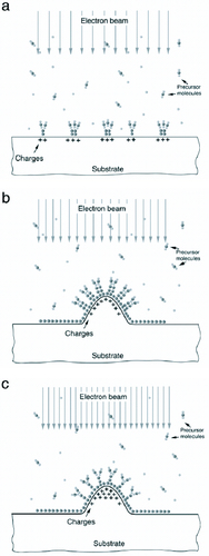
Figures (b) and (c) schematically show the growth conditions of nanodendrites and fractal-like nanotrees, respectively. When the intensity of the EB is markedly increased, an adsorbed molecule on the surface may be decomposed in a very short period before it can move. Hence, a compact layer is deposited on the surface, similar to that observed in figure , shown as a dark contrast in the EB-irradiated area. This results in the entire irradiated area becoming conductive. After this stage, the charges on the surface can move a long distance to the substrate edge, particularly when the surface is convex. A strong electric field is thus generated near the convex surface. Once a deposit grows away from the surface at a point, charges then accumulate there. This deposit thus grows preferentially because the charges attract precursor molecules. When the current density is moderate, the electric field generated near a tip may not strongly affect the trajectory of a molecule. Therefore, the deposit grows at both its tip and its main body because the molecules arrive at the tip and the main body at the same time. Therefore, the main body of the deposit increases in thickness with time and develops a dendritic morphology, as observed in figure . On the other hand, if the intensity of the EB is very strong, the generated electric field will become sufficiently strong to affect the trajectory of a molecule near the tip of a deposit. The molecules are thus likely to be attracted to the tip and are not easily adsorbed on the main body of the deposit. Therefore, a fractal-like tree morphology is formed, as observed in figure .
Characterization of the nanostructures
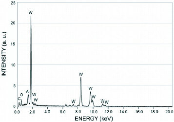
Analyses by energy-dispersive x-ray spectroscopy (EDS) confirmed that the nanodendrites fabricated by EBID using a W(CO)6 precursor contained mainly W, the target element [Citation18, Citation21–23]. An EDS spectrum of the nanodendrites is shown in figure [Citation18]. The composition is similar to that of W deposits fabricated on conductive substrates [Citation6].
Figure 8 An x-ray EDS spectrum obtained from W nanodendrites fabricated on an Al2O3 substrate. (Reproduced with permission from [Citation18], © 2005, Springer Science+Business Media.)
Generally, as-prepared nanostructures contain crystalline grains and an amorphous part. It was confirmed that body-centered cubic (bcc) W nanocrystals are contained in as-prepared W nanowhiskers [Citation20] and W nanodendrites [Citation18, Citation21–23] by high-resolution transmission electron microscopy (HRTEM) and selected-area electron diffraction (SAED) or microbeam electron diffraction (MBED). Figure shows HRTEM and SAED images of W nanodendrites [Citation18]. Crystalline grains can be observed in the nanodendrites. The spacing of the lattice fringe and the angle between the lattice fringes in the grain agree with those of bcc W (figure (a)). Figure (b) shows an SAED pattern obtained from the nanodendrites. Several diffuse rings are observed, indicating the existence of very small crystals in the deposit. These rings correspond to the lattice spacing of bcc W crystals.
Figure 9 An HRTEM micrograph (a) and an SAED pattern (b) of W nanodendrites fabricated on an Al2O3 substrate. The arrows in (a) indicate lattice fringes in grains A and B, which have interfringe angles of 60° (A) and 90° (B), respectively. The diffuse rings in (b) correspond to the lattice spacing of bcc W crystals. (Reproduced with permission from [Citation18] © 2005, Springer Science+Business Media.)
The fraction of crystalline tungsten in W nanodendrites depends on the energy of the EB used in EBID. W nanodendrites were fabricated by a number of applications of EBID in which the energy of the EB was 400, 600, 800 and 1000 keV [Citation23]. The fabricated nanodendrites were characterized by HRTEM. Crystalline grains (bcc W) and amorphous areas were observed. However, the fraction of the amorphous area decreased with increasing energy of the EB. Almost no amorphous area was observed in the nanodendrites fabricated using a 1000 keV EB. Therefore, it was concluded that the crystallization of the nanodendrites improved with increasing energy of the EB. It was also observed that the crystallization of the amorphous part in the as-fabricated W nanodendrites can be realized by irradiation with a high-energy (1000 keV) EB [Citation33]. The irradiation with high-energy electrons promotes the diffusion of W atoms in the amorphous part of the nanodendrites, thus promoting the crystallization [Citation23, Citation33].
It is concluded that the nanostructures fabricated on insulator substrates by EBID have some superior features, such as a large specific surface area, a freestanding structure on substrates, a regular size in nanometers for the tip or the branch, and high purity.
Composite structures of nanodots/nanodendrites
Complex-shape nanostructures have attracted great interest because advanced functional materials might be realized if they can be formed with well-defined three-dimensional (3D) architectures [Citation34–36]. Several multi-element systems, such as Au/Cu and Pt/C composite materials [Citation37, Citation38], have been reported to be useful in catalysts, sensors, energy sources [Citation39, Citation40], and in many other applications. It has been demonstrated that bimetallic bonding can induce significant changes in the properties of the surface, in many cases producing catalysts that have superior activity and/or selectivity [Citation37, Citation38, Citation41, Citation42].
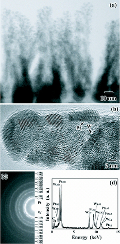
The nanostructures fabricated on insulator substrates by EBID are good base materials for the fabrication of complex-shape nanostructures because of their superior features. Pt nanoparticles or Au nanoparticles were deposited on W nanodendrites fabricated on insulator Al2O3 substrates, and a composite nanostructure consisting of Pt nanoparticles and W nanodendrites (Pt-nanoparticle-decorated W nanodendrites, or Pt nanoparticle/W nanodendrite), or Au nanoparticle and W nanodendrites were fabricated by ion-sputtering [Citation24]. Figure shows the Pt nanoparticle/W nanodendrite composite structures. Figure (a) is a bright-field TEM image of the as-fabricated composite structure produced with EB irradiation with a fluence of 5.0×10²¹ e cm−2 and an ion-sputtering time of 40 s. Figure (b) shows an HRTEM image of the tip of a composite nanostructure. Figure (c) shows the corresponding SAED pattern. Figure (d) shows the EDS spectrum obtained at the tip corresponding to figure (b). By combining TEM observations with EDS analyses of the composite structures, it was confirmed that the Pt nanoparticles were nearly uniformly distributed on the W nanodendrites. Lattice fringes are observed in figure (b). By measuring the lattice spacing and the interfringe angles from this and other images, it was clear that the as-fabricated composite nanostructures consisted of nanocrystals of Pt and W. These nanocrystals were identified to be the equilibrium phases of face-centered cubic (fcc) Pt and bcc W, respectively. Pt and W peaks are dominant in the EDS spectrum although traces of C and O are also observed. Thus, it was confirmed that Pt nanoparticles were effectively grown on the nanodendritic W structures. The average size of the nanoparticles was 2.3 nm. The particle size can be easily controlled by varying the ion-sputtering time. In a similar process, an Au nanoparticle/W nanodendrite composite structure was also fabricated [Citation24].
Figure 10 (a) A bright-field TEM image of as-fabricated Pt nanoparticle/W nanodendrite composite structures on an Al2O3 substrate, (b) the HRTEM image, (c) the SAED pattern, and (d) the EDS spectrum taken from the tip of the composite nanostructures. (Reproduced with permission from [Citation24], © 2006, American Institute of Physics.)
Using this process, various other metal composite nanoparticle/nanodendrite structures, such as Mo/W and Au/Pt, can also be fabricated. Therefore, the technique may be easily employed to fabricate metal nanoparticle/nanodendrite compound nanostructures of a wide range of materials. Because the nanodendrite structure possesses a comparatively large specific surface area, it has potential applications for catalysts, sensors and gas storages.
Structures fabricated using other precursors
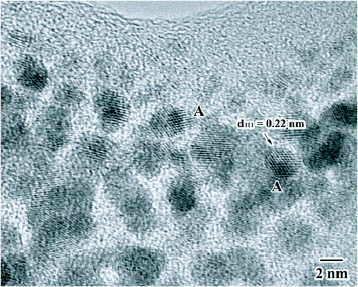
Organic or organometallic substances with appropriate vapor pressure can be used as precursor materials for EBID [Citation7]. It is expected that various precursors can be used to fabricate nanostructures on insulator substrates by EBID. Pt deposition was carried out on insulator Al2O3 substrates by EBID in a TEM [Citation43]. (Methylcyclopentadienyl)trimethylplatinum powder, Me3MeCpPt, was used as the precursor. Pt nanodendritic structures were fabricated in the area of EB irradiation, as shown in figure . The intensity and fluence of the EB were 3.2×10¹⁸ e cm−2 s−1 (0.51 A cm−2) and 2.0×10²⁰ e cm−2, respectively. The dendrites show a tendency to grow at the edge of the substrate. The typical thickness of the tips is less than 3 nm, as observed in figure (b). TEM observation, diffraction pattern analyses, and EDS analyses indicate that a nanodendrite structure with a high Pt content was formed. Figure shows an HRTEM micrograph of the fabricated Pt nanodendrite [Citation43]. It was confirmed that fcc Pt nanoparticles and an amorphous part were contained in the structure. The morphology of the Pt nanodendrite is considerably different from that of the W nanodendrite fabricated on an Al2O3 substrate, suggesting that the growth of a nanodendrite depends largely on the properties of the precursor.
Figure 11 (a) A TEM micrograph of Pt nanodendrite structures grown on the surface of an Al2O3 substrate by EBID for 1 min with an electron fluence of 2.0×10²⁰ e cm−2; (b) the enlargement of the square area in (a) showing the nanodendrite in more detail. (Reproduced with permission from [Citation43], © 2006, Springer Science+Business Media.)
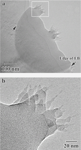
Figure 12 An HRTEM micrograph of Pt nanodendrite structures grown on the surface of an Al2O3 substrate by EBID with an electron fluence of 2.6×10²¹ e cm−2. (Reproduced with permission from [Citation43] © 2006, Springer Science+Business Media.)
Subjects for further study
EBID on insulator substrates is a simple but a promising technique because nanostructures with characteristic morphologies can be fabricated. The nanostructures have some advanced features, as mentioned in section 6. Furthermore, there are many possible combinations of precursor and substrate; therefore, various functional nanostructures or compound nanostructures can be fabricated. The nanostructures may be used in technologies such as catalysts, gas sensors, electron emitters, and the connection of electric units in 3D integrated circuits. However, to apply EBID for the fabrication of various functional nanostructures, some subjects should be further studied. Although the formation of the different morphologies of the nanostructures can be understood qualitatively on the basis of the proposed mechanisms, some details on the growth and formation of the nanostructures are still not clear. For example, it is still not known why the nanostructures only grow on the narrow area of the insulator substrate, and why the typical thickness of a nanowhisker, the tip of a nanodendrite, and the tip of a nanotree is about 3 nm. Also, the growth conditions required for each combination of precursor and substrate seem to be different and should be investigated. These subjects relate to the fundamental processes involved in the interaction of an EB with insulators, the adsorption of precursor molecules on a substrate, and the decomposition of molecules by energetic electrons. Obtaining the answers to these questions will be very helpful for controlling the growth processes of the nanostructures.
Conclusions
Utilizing the condition that charges accumulate on an insulator substrate upon EB irradiation, characteristic nanostructures such as arrays of nanowhiskers and nanodendrites and fractal-like nanotrees, can be fabricated by EBID. The typical diameter of a nanowhisker, the tip of the nanodendrite, and the tip of the nanotree is about 3 nm, and has little dependence on the fabrication conditions such as the size and intensity of the EB. It was demonstrated for W nanostructures that nanostructures with different morphologies can be obtained by controlling the intensity of the EB during EBID. The growth process of the different nanostructures has been explained qualitatively. The nanostructures have advanced features such as a large specific surface area, a freestanding structure on substrates, a typical size of several nanometers, and high purity. Because there are many possible combinations for the precursor and substrate, it is expected that various nanostructures may be fabricated on various substrates. The nanostructures can be easily decorated by metallic nanoparticles to form composite structures such as the Pt nanoparticle/nanodendrites. Therefore, the nanostructures and their fabrication process may be applied in technology to realize various functional nanomaterials such as catalysts, sensor materials, and emitters. However, there are also some subjects that should be further studied before their actual application, for example, fabrication of nanowhiskers over large areas of a substrate and the controlled growth of nanostructures for each combination of precursor and substrate.
References
- AlivisatosA P 1996 Science 271 933 http://dx.doi.org/10.1126/science.271.5251.933
- ZhangH FWangC MBuckE CWangL S 2003 Nano Lett. 3 577 http://dx.doi.org/10.1021/nl0341180
- ShiZ JLianY FLiaoF HZhouX HGuZ NZhangTIijimaSLiH DYueK TZhangS L 2000 J. Phys. Chem. Solids 61 1031 http://dx.doi.org/10.1016/S0022-3697(99)00358-3
- DaiZ RPanZ WWangZ L 2003 Adv. Funct. Mater. 13 9 http://dx.doi.org/10.1002/adfm.200390013
- JinYTangK BAnC HHuangL Y 2003 J. Cryst. Growth 253 429 http://dx.doi.org/10.1016/S0022-0248(03)00997-7
- KoopsH W PWeielRKernD PBaumT H 1988 J. Vac. Sci. Technol. B 6 477 http://dx.doi.org/10.1116/1.584045
- KoopsH W PKretzJRudolphMWeberMDahmGLeeK L 1994 Japan J. Appl. Phys. Part 1 33 7099 http://dx.doi.org/10.1143/JJAP.33.7099
- HoyleP CCleaverJ R AAhmedH 1996 J. Vac. Sci. Technol. B 14 662 http://dx.doi.org/10.1116/1.589154
- HiroshimaHSuzukiNOgawaNKomuroM 1999 Japan J. Appl. Phys. 38 7135 http://dx.doi.org/10.1143/JJAP.38.7135
- Kohlmann-von PlatenK TChiebekJWeissMReimerKOertelHBrüngerW H 1993 J. Vac. Sci. Technol. B 11 2219 http://dx.doi.org/10.1116/1.586460
- MatsuiSIchihashiT 1988 Appl. Phys. Lett. 53 842 http://dx.doi.org/10.1063/1.100089
- MitsuishiKShimojoMHanMFuruyaK 2003 Appl. Phys. Lett. 83 2064 http://dx.doi.org/10.1063/1.1611274
- AllenT EKunzR RMayerT M 1988 J. Vac. Sci. Technol. B 6 2057 http://dx.doi.org/10.1116/1.584111
- TanakaMShimojoMHanMMitsuishiKFuruyaK 2005 Surf. Interface Anal. 37 261 http://dx.doi.org/10.1002/sia.1978
- BanhartF 1995 Phys. Rev. E 52 5156 http://dx.doi.org/10.1103/PhysRevE.52.5156
- ZhangJ ZYeX YYangX JLiuD 1997 Phys. Rev. E 55 5796 http://dx.doi.org/10.1103/PhysRevE.55.5796
- WangH ZLiuX HYangX JWangX 2001 Mater. Sci. Eng. A 311 180 http://dx.doi.org/10.1016/S0921-5093(01)00916-9
- SongMMitsuishiKTanakaMTakeguchiMShimojoMFuruyaK 2005 Appl. Phys. A 80 1431 http://dx.doi.org/10.1007/s00339-004-2997-z
- SongMMitsuishiKFuruyaK 2005 Ceramic Nanomaterials and Nanotechnology: Ceramic Transactions vol 159 New York Wiley p 31
- SongMMitsuishiKFuruyaK 2007 Mater. Trans. 48 2551 http://dx.doi.org/10.2320/matertrans.MD200717
- XieGSongMMitsuishiKFuruyaK 2005 Japan J. Appl. Phys. 44 5654 http://dx.doi.org/10.1143/JJAP.44.5654
- XieGSongMMitsuishiKFuruyaK 2005 J. Nanosci. Nanotechnol. 5 615 http://dx.doi.org/10.1166/jnn.2005.075
- XieGSongMMitsuishiKFuruyaK 2005 Physica E 29 564 http://dx.doi.org/10.1016/j.physe.2005.06.028
- XieGSongMFuruyaKLouzguineD VInoueA 2006 Appl. Phys. Lett. 88 263120 http://dx.doi.org/10.1063/1.2217261
- SongMMitsuishiKTakeguchiMFuruyaK 2005 Appl. Surf. Sci. 241 107 http://dx.doi.org/10.1016/j.apsusc.2004.09.026
- SongMMitsuishiKFuruyaK 2005 Physica E 29 575 http://dx.doi.org/10.1016/j.physe.2005.06.030
- WintersH FInokutiM 1982 Phys. Rev. A 25 1420 http://dx.doi.org/10.1103/PhysRevA.25.1420
- SeuretPCicoiraFOhtaTDoppeltPHoffmannPWeberJWesolowskiT A 2003 Phys. Chem. Chem. Phys. 5 268 http://dx.doi.org/10.1039/b206731e
- FowlkesJ DRandolphS JRackP D 2005 J. Vac. Sci. Technol. B 23 2825 http://dx.doi.org/10.1116/1.2101732
- Silvis-CividjianNHagenC WKruitPStamM A J v dGroenH B 2003 Appl. Phys. Lett. 82 3514 http://dx.doi.org/10.1063/1.1575506
- Silvis-CividjianNHagenC WKruitP 2005 J. Appl. Phys. 98 84905–1 http://dx.doi.org/10.1063/1.2085307
- MitsuishiKLiuZ QShimojoMHanMFuruyaK 2005 Ultramicroscopy 103 17 http://dx.doi.org/10.1016/j.ultramic.2004.11.011
- SongMMitsuishiKFuruyaK 2005 Mater. Sci. Forum 475–479 4035
- GaoP XDingYMaiWHughesW LLaoCWangZ L 2005 Science 309 1700 http://dx.doi.org/10.1126/science.1116495
- DickK ADeppertKLarssonM WMartenssonTSeifertWWallenbergL RSamuelsonL 2004 Nat. Mater. 3 380 http://dx.doi.org/10.1038/nmat1133
- LiHSchnableggerMMannS 1999 Nature 402 393 http://dx.doi.org/10.1038/46509
- PalURamirezJ F SLiuH BMedinaAAscencioJ A 2004 Appl. Phys. A 79 79 http://dx.doi.org/10.1007/s00339-003-2478-9
- JooS HChoiS JOhIKwakJLiuZTerasakiORyooR 2001 Nature 412 169 http://dx.doi.org/10.1038/35084046
- RuizAArbiolJCireraACornetAMoranteJ R 2005 Mater. Sci. Eng. C 19 105 http://dx.doi.org/10.1016/S0928-4931(01)00451-9
- De MeijerR J et al 1997 Nanostruct. Mater. 8 205 http://dx.doi.org/10.1016/S0965-9773(97)00009-3
- WangALiuJLinSLinTMouC 2005 J. Catal. 233 1486
- LiuPRodriguezJ AMuckermanJ THrbekJ 2003 Surf. Sci. 530 L313 http://dx.doi.org/10.1016/S0039-6028(03)00023-2
- XieGSongMMitsuishiKFuruyaK 2006 J. Mater. Sci. 41 2567 http://dx.doi.org/10.1007/s10853-006-7769-z