Abstract
A stable superhydrophobic copper surface was obtained by radio-frequency magnetic sputtering on Si (100) and quartz substrates. The water contact angle and sliding angle of the superhydrophobic copper surface were 160.5° and 3±1.9°, respectively. Scanning electron microscopy (SEM) photos show that the superhydrophobic surface structure comprises many uniform nanocrystals with a diameter of about 100 nm. A brief explanation of the formation of this special microstructure and the mechanism of its wettability were proposed.
Introduction
Controlling the wettability of surfaces is an important problem relevant to many areas of technology [Citation1]. A surface having a water contact angle greater than 150° is commonly called superhydrophobic [Citation2]. Given the limited contact area between the solid surface and the water, chemical reactions or bonding formation through water are limited on a superhydrophobic surface. Accordingly, various phenomena such as the adherence of snow, oxidation and current conduction are expected to be inhibited on such a surface [Citation3]. In addition, the nonwettable character of superhydrophobic surfaces has been applied in biomedical applications ranging from blood vessel replacement to wound management [Citation1]. Thus, superhydrophobic surfaces have many potential applications in industrial, agricultural, and biomedical fields.
In general, the wettability of a solid surface is governed by both the chemical state and the geometry of the morphology [Citation4, Citation5]. Recently, superhydrophobic surfaces have been fabricated successfully with micro- or nanostructured polymer surfaces by mimicking superhydrophobic designs found in nature [Citation6–9]. Corresponding to the development of microfluidic devices [Citation10–12], other characteristics such as optical or electrical properties are required simultaneously with surface superhydrophobicity. Moreover, for many applications, organic materials are not suitable due to their weak thermal and mechanical stability [Citation13, Citation14]. Besides their good physical and mechanical properties, copper films have high diathermanous and electric performances [Citation15]. Combined with their special wettability properties, copper films are highly suitable for the integration of microfluidic transportations, chemical reactions and electrical tests in a single chip.
However, to fully utilize the hydrophobic properties of nanostructured surfaces, it is necessary to study the fundamental relationship between the nanostructure and the hydrophobic behavior. Once the relationship is established, new materials with desired hydrophobicity can be designed and fabricated. Sputtering is a simple and useful technique for preparing thin films with a desired structure and properties. In the present work, copper films with different microstructures were prepared by magnetron sputtering on Si (100) and quartz substrates, and the deposition processes were controlled to adjust the morphology of the surfaces of the Cu films. The wetting properties of these copper layers with different morphologies were studied by contact angle measurement.
Experimental
Materials used and preparation of superhydrophobic copper surface
Copper thin films with different microstructures were produced on Si (100) and quartz substrates using a JS-450 magnetron sputtering system at various sputtering powers. The target used was a copper (99.99% purity) plate of 10 cm diameter. Sputtering was carried out in Ar (99.99% purity) plasma under a working pressure of 0.5 Pa. The substrate temperature was room temperature and the sputtering power was from 100 to 400 W with a fixed target-substrate distance of 6 cm.
Characterization
The surface morphology of these films was studied by scanning electron microscopy (SEM JEOL JSM6500) at an accelerating voltage of 30 kV. X-ray photoelectron spectrometry (XPS) analyses of the samples were performed on a PHI 5600 spectrometer with a monochromatic AlKα source at 14 kV and 350 W, and the photoelectron take-off angle was 45°. The structure of the thin films was characterized by x-ray diffraction (XRD) measurements. The surface roughness of films was measured using Step Apparatus (Nanopics, Japan). The wettability of the copper surfaces was measured using a GonioStar contact angle system at ambient temperature. The equilibrium contact angles of 5 μL water droplets were measured by the sessile drop method. The advancing and receding contact angles were measured as follows: a 5 μL water droplet was placed on the sample using a syringe, and the advancing contact angle was recorded by increasing the water volume to 8 μL at a rate of 0.3 μL s−1, then the receding contact angle was recorded by decreasing the water volume at the same rate. The parameters and performances of the copper films prepared in our experiments are listed in table 1.
Parameters of prepared and performance of copper films.
Results and discussion
SEM results
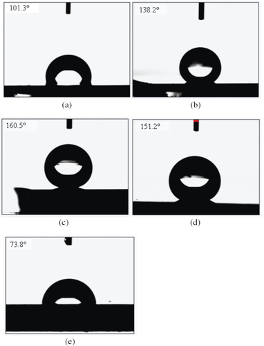
The artificial surfaces exhibit different wettability, ranging from 101.3 to 160.5°, which is dependent on geometry of their microstructures. The ability to easily control the hydrophobicity and superhydrophobicity of copper films provides an opportunity for further understanding the relationship between the surface wettability and the morphology. Thus, these surfaces may be promising materials for practical applications. Figure shows SEM images of the films prepared at a power of 200 W, and the water contact angle is 160.5° on this surface. Figure shows SEM images of the films prepared at various powers. It is evident that the sputtering power plays an important role in the formation of surfaces with different morphologies, which is considered to result from the diffusion and collision of atoms with different energies that are sputtered onto the substrate during the deposition at different powers. Figures (e) and (f) show high-resolution SSEM images of the copper film prepared at a sputtering power of 200 W; the volume of each crystal is about 100 nm and these nanocrystals form an interstitial nanostructure. The surface roughnesses of films (a), (b), (c) and (d) are 62, 79, 161 and 112 nm, respectively. As the working power increases, the crystal volume also increases, and the water contact angle first increases and then decreases. Figure shows that the water contact angles on surfaces formed at various deposition powers. The water contact angles are 101.3° (a, 400 W), 138.2° (b, 300 W), 160.5° (c, 200 W), 151.2° (d, 100 W) and 73.8° (e, polished copper film).
Figure 1 (A) SEM image of hydrophobic copper film with nanoparticles prepared at 200 W power. (B) Photograph of a water drop on the superhydrophobic copper surface in (A).
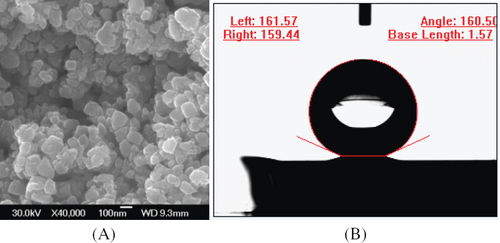
Figure 2 SEM images of copper films prepared at various sputtering powers. (a) 400 W, (b) 300 W, (c) 200 W and (d) 100 W. (e) and (f) High-resolution SEM images of copper prepared at sputtering power of 200 W.
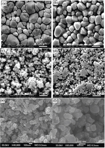
Figure 3 Water contact angles measured on the surface of copper film at various sputtering powers: (a) 400 W, (b) 300 W, (c) 200 W, (d) 100 W and (e) polished copper film. The water contact angles are 101.3°, 138.2°, 160.5°, 151.2° and 73.8°, respectively.
XRD and XPS results
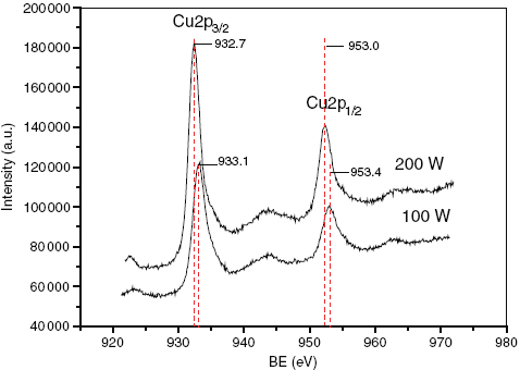
The crystal structure and the orientation of the copper thin films were investigated by XRD analysis. Figure shows the XRD spectra of copper thin films deposited at different sputtering powers. As the sputtering power increases, the intensities of (111) and (200) peaks also intensified. Meanwhile, diffraction peaks appeared at 2θ=74° and 91°, respectively, corresponding to (220) and (531) planes of copper, which also intensified with increasing sputtering power. When the sputtering power decreased to 200 W, the (311) peak almost vanished but the other peaks remained in the XRD patterns. It is evident that increasing the sputtering power results in increases in diffraction peak intensities and the volume of copper crystals. Determining the chemical state of the species on the surface is important for establishing the properties causing the wettability. For this purpose, XPS analysis was carried out to obtain information on the composition of the mixed oxides on the Cu films of two samples. The surfaces of films (c) and (d), corresponding to sputtering powers of 200 W and 100 W, respectively, were analyzed by XPS (figure ). The peaks at 953.0 and 932.7 eV correspond to the binding energy of Cu 2p [Citation16]. However, the peaks at 953.4 and 933.1 eV indicate the existence of Cu2O in the films. Because of its lower deposition rate, film (d) contains oxygen and film (c) contains only pure elemental copper. Although the wetting property is affected by both the chemical state and the morphology of the surface, herein, the main reason that film (c) is more hydrophobic than film (d) results from its interstitial cottonlike nanostructure, and the unique geometry of the microstructures ensures that there is sufficient roughness to trap enough air to repel water drops.
Figure 4 XRD patterns of copper films prepared at different sputtering powers. (a) 400 W, (b) 300 W, (c) 200 W and (d) 100 W.
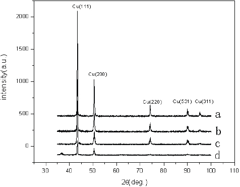
Figure 5 XPS spectra of copper films prepared at sputtering powers of 100 and 200 W.
Calculation results
Clearly, the microstructures of film (c) markedly increase the surface roughness: thus, the air–liquid interface should be crucial for increasing the contact angle. It is suggested that air can be easily trapped by the microstructures on the surface, and then water cannot intrude into the interspaces among the microstructures. These surfaces, consisting of the trapped air and the solid, can be regarded as ‘composite’ surfaces. According to the Cassie-Baxter mode [Citation17–19], contact angle, θr, is related to the features in the microstructure apparent on the rough surface in the SEM images by
(1)
where θs is the equilibrium contact angle of the flat surface, and f1 and f2 are the solid–liquid contact fraction and air–liquid contact fraction (i.e. f1+f2=1), respectively. To further determine the reason for the superhydrophobicity of the interface, a contrasting experiment involving the measurement of the contact angle on a smooth film surface was performed. Given the contact angle (θs=73.8°) on the copper film with a smooth surface, the values of f2 for copper films (c) and (d) were obtained as 0.94 and 0.81, respectively. Through these f2 values, we conclude that the trapped air within the microstructures is important for the production of superhydrophobicity. In other words, the cottonlike nanostructure can enhance the fraction of air that is contained within the ‘valleys' between the protrusions on the surface, which plays a very important role in the fabrication of a superhydrophobic surface.
Water sliding angle results
To determine whether a surface is superhydrophobic, the sliding angle of a water droplet on the surface is also an important criterion [Citation1]. In practice, surfaces always have two contact angles, the advancing contact angle and the receding contact angle, due to factors such as the unevenness, contamination, motility, swelling, rigidity, roughness, and nonhomogeneity of the solid surface composition [Citation20–23]. The sliding angle can is defined as the difference between the advancing contact angle and the receding contact angle. Recently, in some papers the relationship between the surface roughness and the sliding angle (contact angle hysteresis) has been discussed [Citation20–24]. Öner and coworkers [Citation20, Citation21] argued that the structure of the three-phase contact line was important for determining the advancing and receding contact angles; discontinuous, unstable and contorted contact lines were necessary to form a superhydrophobic surface with low hysteresis. In addition, Miwa et al [Citation22] concluded that surface structures that can trap air were important for the preparation of low-sliding-angle surfaces. According to the SEM image of the as-prepared copper surface (figure (c)), the three-phase contact line is discontinuous on the surface and the porous surface structure can trap air, suggesting that the as-prepared copper surface should have a low contact angle hysteresis and that a water droplet can slide easily on the surface. Thus, we measured the advancing contact angle and receding contact angles. The advancing contact angle was obtained by adding water to increase water droplet volume, and the receding contact angle was obtained by sucking off the water to decrease the water droplet volume. The magnitude of the water sliding angle was about 3±1.9° (similar to the sliding angle of a lotus leaf), indicating that a water droplet can roll easily on the superhydrophobic porous copper surface (film (c)). We also carefully tilted the superhydrophobic copper surface to determine the sliding angle. When the surface was tilted about 3°, the water droplet began to slide, showing the same result as the above water sliding angle (contact angle hysteresis).
Conclusions
A stable superhydrophobic copper surface was obtained directly on Si (100) and quartz substrates without the addition of low-surface-energy compounds by a new simple approach. The water contact angle and sliding angle of the as-prepared superhydrophobic copper surface were 160.5° and 3±1.9°, respectively. Furthermore, the superhydrophobic copper surface still exhibited high diathermanous and electric performances, which may widen the applicability of this copper surface. Compared with other methods of synthesizing superhydrophobic surfaces, the present method is much simpler to control, without the need for any complicated processes. The method can also be easily scaled up to create large-area uniform superhydrophobic surface structures and can be applied in commercial manufacturing.
Acknowledgments
This work was supported by the Beijing Technology New Stars Project (2004A10), the Scientific Research Common Program of the Beijing Municipal Commission of Education (KM200310005011), PHR(IHLB), the Beijing Specific Project to Foster Elitist (no. 20041D0501513), the Beijing Natural Science Foundation (no. 2062004) and the National Natural Science Foundation of China (no. 50502001, no. 60576012).
References
- MaMHillR M 2006 Curr. Opin. Colloid Interface Sci. 11 193 http://dx.doi.org/10.1016/j.cocis.2006.06.002
- OndaTShibuichiSSatohNTsujiiK 1996 Langmuir 12 2125 http://dx.doi.org/10.1021/la950418o
- NakajimaAFujishimaAHashimotoKWatanabeT 1999 Adv. Mater. 11 1365 http://dx.doi.org/10.1002/(SICI)1521-4095(199911)11:16<1365::AID-ADMA1365>3.0.CO;2-F
- RyuD YShinKDrockenmullerEHawkerC JRussellT P 2005 Science 308 236 http://dx.doi.org/10.1126/science.1106604
- GenzerJEfimenkoK 2000 Science 290 2130 http://dx.doi.org/10.1126/science.290.5499.2130
- FengLSongYZhaiJLiuBXuJJiangLZhuD 2003 Angew. Chem. Int. Ed. 42 800 http://dx.doi.org/10.1002/anie.200390212
- XieQFanGZhaoNGuoXXuJDongJZhangLZhangYHanC C 2004 Adv. Mater. 16 1830 http://dx.doi.org/10.1002/adma.200400074
- YuXWangZJiangYShiFZhangX 2005 Adv. Mater. 17 1289 http://dx.doi.org/10.1002/adma.200401646
- ShirtcliffeN JMchaleGNewtonM IChabrolGPerryC C 2004 Adv. Mater. 16 1929 http://dx.doi.org/10.1002/adma.200400315
- KenisP J AIsmagilovR FWhitesidesG M 1999 Science 285 83 http://dx.doi.org/10.1126/science.285.5424.83
- PrinsM W JWeltersW J JWeekampJ W 2001 Science 291 277 http://dx.doi.org/10.1126/science.291.5502.277
- MeldrumD RHollM R 2002 Science 296 1197 http://dx.doi.org/10.1126/science.297.5584.1197
- FengXFengLJinMZhaiJJiangLZhuD 2004 J. Am. Chem. Soc. 126 62 http://dx.doi.org/10.1021/ja038636o
- YanHKurogiKMayamaHTsujiiK 2005 Angew. Chem. Int. Ed. 44 3453 http://dx.doi.org/10.1002/anie.200500266
- LiMZhaiJLiuHSongYJiangLZhuD 2003 J. Phys. Chem. B 107 9954 http://dx.doi.org/10.1021/jp035562u
- WagnerC D 1979 Handbook of X-ray Photoelectron Spectroscopy Minnesota Perkin-Elmer
- CassieA B D 1948 Trans. Faraday Soc. 44 11
- PatankarN A 2004 Langmuir 20 8209 http://dx.doi.org/10.1021/la048629t
- MarmurA 2004 Langmuir 20 3517 http://dx.doi.org/10.1021/la036369u
- ChenWFadeevA YHsiehM CÖnerDYoungbloodJ PMcCarthyT J 1999 Langmuir 15 3395 http://dx.doi.org/10.1021/la990074s
- ÖnerDMcCarthyT J 2000 Langmuir 16 7777 http://dx.doi.org/10.1021/la000598o
- MiwaMNakajimaAFujishimaAHashimotoKWatanabeT 2000 Langmuir 16 5754 http://dx.doi.org/10.1021/la991660o
- MabbouxFPonsonnetLMorrierJ JJaffrezicNBarsottiO 2004 Colloids Surf. B: Biointerfaces 39 199 http://dx.doi.org/10.1016/j.colsurfb.2004.08.002
- MhamdiLPicartCLagneauCOthmaneAGrosgogeatBJaffrezic-RenaultNPonsonnetL 2006 Mater. Sci. Eng. C: Biomim. Mater. Sens. Syst. 26 273