Abstract
We describe an alternative method for realizing a carbon nanotube spin field-effect transistor device by the direct synthesis of single-walled carbon nanotubes (SWNTs) on substrates by alcohol catalytic chemical vapor deposition. We observed hysteretic magnetoresistance (MR) at low temperatures due to spin-dependent transport. In these devices, the maximum ratio in resistance variation of MR was found to be 1.8%.
Introduction
Carbon nanotubes (CNTs) are considered to be a potential material for spin electronics device applications. They exhibit a long electron mean free path [Citation1, Citation2] and weak spin-orbit coupling; thus, the spin diffusion length is expected to be extremely large [Citation3]. Spin-dependent transport in carbon nanotubes was originally demonstrated in multi-walled carbon nanotubes (MWNTs) with ferromagnetic contacts [Citation4]. For spin electronics application, however, single-walled carbon nanotubes (SWNTs) have many advantages over MWNTs. A greater spin diffusion length and a well-defined electron band structure can be expected in SWNTs. In this paper, we report the direct fabrication of SWNTs on patterned substrates by alcohol catalytic chemical vapor deposition (ACCVD) to form spin field-effect transistor (FET) devices, and we discuss their magnetoresistance (MR) behavior. We adopt a Co catalyst for SWNT growth, which also acts as a ferromagnetic contact, to inject a spin-polarized current inside the nanotube in order to observe any MR effects.
Experimental details
Device fabrication and catalyst preparation
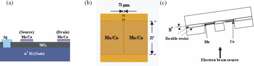
In the direct synthesis of SWNTs in FETs, a Mo/Co bilayer was used both as the catalyst for the SWNT growth and as ferromagnetic electrodes. The FETs fabricated in this study had the back-gate configuration, as shown in figure (a). A heavily doped n-type silicon wafer with a 400-nm-thick thermally oxidized SiO2 layer on the surface was used as the substrate. The SiO2 layer and the doped silicon layer of the wafer were used as the gate insulator and gate electrode, respectively. The source and drain electrodes were patterned on the insulating SiO2 layer by photolithography. The channel length L was fixed at 5 μm and the channel widths W were designed to be 250 and 500 μm, as shown in figure (b). Mo was first deposited on the substrate using an electron-beam evaporation system to a thickness of 100 nm. After the deposition of Mo, the substrate was subsequently tilted 8° for the following deposition of the Co catalyst, as illustrated in figure (c). The Co catalyst was then deposited using the electron-beam evaporation system to a nominal thickness of 1 nm. The tilted deposition technique shown in figure (c) was also employed to deposit Co on the side of the Mo to enhance the growth of SWNTs along the channel.
Figure 1 (a) Schematic drawing of device structure, (b) optical microscope image of Mo/Co electrodes on the n+-Si/SiO2 substrate, (c) schematic drawing of setup for the angled deposition of Co.
SWNT synthesis by ACCVD
SWNTs were synthesized on the Co catalyst by ACCVD with ethanol as a feed gas. After the catalyst was deposited, the substrate was subsequently transferred to the CVD reactor. The reactor was evacuated by a rotary pump to a pressure of 1 Pa, while the furnace was heated to 900 °C at a position 30 cm away from the substrate. A mixed gas flow of Ar/H2 (3% H2) was used to purge the CVD reactor at an internal pressure of 200 Pa. When the furnace temperature reached the synthesis temperature, the furnace was immediately transferred to the substrate position for rapid heating [Citation5]. The Ar/H2 gas flow was then terminated and ethanol was immediately fed into the reactor at a flow rate of 6.0 litre/min−1 to start the decomposition of ethanol. The catalytic reaction of ethanol continued for 30 min. During the reaction, the internal pressure of the CVD reactor was 3.2 kPa. After the synthesis, the furnace was removed from the substrate position and the ethanol gas flow was stopped. The substrate was left to cool naturally. The quartz tube used for this reactor was 1200 mm in length and 26 mm in inner diameter. The SWNTs grown on the substrate were characterized by scanning electron microscopy (SEM, Hitachi S4100), atomic force microscopy (AFM, Seiko Instruments) and Raman spectroscopy with a laser excitation energy of 632.8 nm (Tokyo Instruments, Nanofinder 30).
Electric conductivity and spin transport
The resistance between the source and drain electrodes was measured by the two-terminal method using a resistance bridge (Picowatt AVS-47) with an excitation voltage of 3 mV and a frequency of 15 Hz. For reference, the resistance of patterned electrodes on substrates before ACCVD was also measured to exclude the extrinsic effects of the current flow. The devices were mounted in a continuous-flow helium cryostat. The MR measurements were performed by setting the cryostat in an electromagnet system. The magnetic field was applied parallel to the tube axis in the plane of the substrate [Citation6]. Measurements were carried out at room temperature and at 4.5 K. The field was swept from 0 to 2000 Oe, then back to −2000 Oe, and measurement stopped at 2000 Oe. As a control experiment, we also measured the MR effect in one of the electrodes.
Results and discussion
Figure (a) shows an SEM image around and between a pair of Mo/Co electrodes after ACCVD. The left and right edges correspond to the Mo/Co electrodes. Fine structures between the electrodes were observed, some of which successfully bridged the electrodes. These fine structures were confirmed to be SWNTs, as discussed below. SWNTs grew from Co nanoparticles that formed at high temperatures during the synthesis. The Co nanoparticle size distribution was estimated by Gaussian fitting to be 6.6±3.3 nm. It was confirmed that almost 500 bundles consisting of 1--10 SWNTs bridge the electrodes. The nanotubes between the electrodes were successfully grown only for the device made by the angled deposition technique, as shown in figure (c). Figure (b) shows another SEM image of a different area between the electrodes used to clarify the nature of the SWNT/Co contacts. The image clearly shows that the SWNTs are in direct contact with Co nanoparticles at both electrodes. To determine the quality of the nanotubes synthesized by this method, Raman spectroscopy measurements were performed. Figure shows Raman spectra obtained at constant intervals around the boundary of an electrode. The Raman spectra exhibit radial breathing mode (RBM) peaks from 100 to 350 cm−1, which are characteristic of SWNTs, and G-band peaks at approximately 1590 cm−1. The strong peak at approximately 500 cm−1 originates from the Si substrate. Although there are some peaks appearing in the D-band region, RBM and G-band peaks are dominant, and they match those in typical Raman spectra of SWNTs. From these results, it is concluded that the SWNTs can be successfully grown to bridge the pair of Mo/Co electrodes by ACCVD, as presented in sections 2.1 and 2.2.
Figure 2 SEM image around and between a pair of Mo/Co electrodes, (b) SEM image of the area between the electrodes showing contacts between nanotubes and Co nanoparticles.
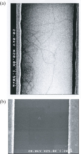
Figure 3 Raman spectra obtained at intervals of 500 nm around the boundary of the electrode.
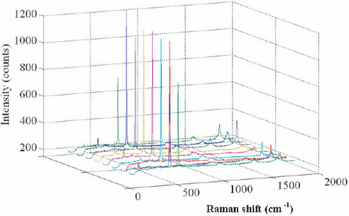
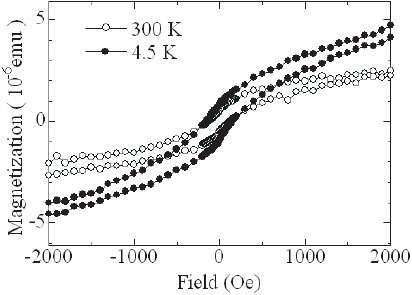
Figure shows the magnetic properties of the device measured by a superconducting quantum interference device (SQUID), which confirmed that the magnetic properties of Co ferromagnetic components remain unchanged at room temperature and at 4.5 K. The coercive force obtained from the hysteresis curve for both temperatures is about 120 Oe. Although Co forms fine nanoparticles on bulk Mo after annealing, its macroscopic magnetic properties are unchanged.
Figure 4 Magnetic properties of device after SWNT synthesis at 300 and 4.5 K.
Current I versus voltage V characteristics for the devices before and after ACCVD are shown in figure . A pronounced enhancement in current was observed for the devices after SWNT growth by ACCVD, whereas no current was observed in the device before ACCVD. We can conclude that the current flows through the SWNTs connecting the pair of electrodes. The resistance of the SWNT devices is about 10–200 Ω at room temperature. Although resistance increases with decreasing temperature, as shown in figure (b), it does not show activation-type temperature dependence. Therefore, the dominant current paths do not consist of semiconducting SWNTs. In agreement with this, no gate voltage dependence was observed. Note that two types of samples were synthesized by ACCVD, which exhibit either high resistance or low resistance. High-resistance samples show good FET characteristics [Citation7]. These facts also suggest that the channels consist of metallic or semiconducting SWNTs, but not other conductive carbon materials. In this study, we mainly focused on the devices with low resistance.
Figure 5 (a) Current versus voltage plots for the fabricated devices before and after ACCVD, (b) temperature dependence of resistance for the device fabricated by ACCVD.
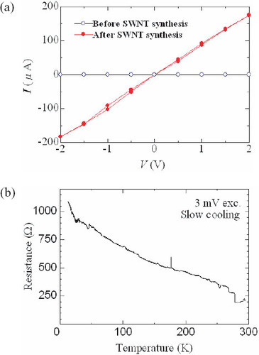
Figure (a) shows that resistance of a device with a channel width of 500 μm at 300 K is almost constant against magnetic field at 186 Ω. However, figure (b) shows that resistance at 4.5 K peaks at approximately 0 Oe, and the peak varies slightly on the direction of the sweep. When the field was swept upward, a peak appeared at about −110 Oe, and when it was swept downwards, a peak appeared at about 110 Oe. For the device with a channel width of 250 μm, similar behaviour was observed to that in the device with the channel width of 500 μm, as shown in figures (a) and (b). To ensure that this MR effect is not governed by the MR of Co nanoparticles on the electrodes, a control experiment was conducted. We measured the MR effect for one of the electrodes at the same temperatures. As a result, no significant change in resistance was observed. This indicates that the hysteretic MR does not originate from the Co nanoparticles themselves. Although the Co ferromagnetic component is independent of temperature, as mentioned above, MR effects were observed at a low temperature. For spin transport without spin scattering through a material connected to two ferromagnetic electrodes, the resistance is high when the ferromagnetic moments in the two electrodes are antiparallel, and low when the ferromagnetic moments are parallel [Citation8]. The spin-valve effect observed in MWNTs [Citation4, Citation9, Citation10] and SWNTs [Citation9, Citation10] is well explained by this model. Our result in this work, however, cannot be simply explained by this model. SWNTs seem to grow from Co nanoparticles, which form from Co thin film on Mo film during ACCVD [Citation11]. Therefore, spin-dependent transport is expected to be governed by the magnetic properties of Co nanoparticles to which the SWNTs are attached and to be strongly dependent on the size of the Co nanoparticles. Each SWNT is attached to a Co nanoparticle with a different size. Thus, it is expected that each SWNT should show MR peaks at different field values where parallel and antiparallel magnetization configurations of the electrodes change. However, the magnetic property of an individual Co nanoparticle in contact with an SWNT cannot be determined. In this study, the average magnetic properties and MR effects of Co nanoparticles were observed. The sharp peaks of averaged MR at approximately ±110 Oe correspond to the average coercive force measured by the SQUID. The origin of this unusual MR hysteresis still remains unclear, but the results of the MR effects are reproducible. A detailed analysis of the spin transport mechanism of these devices is to be carried out in the near future.
Figure 6 Magnetoresistance for the device with W=500 μm at (a) 300 K and (b) 4.5 K. The closed circles (open circles) correspond to the positive (negative) sweep direction.
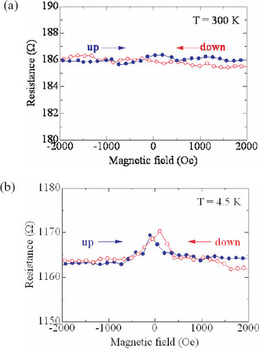
Figure 7 Magnetoresistance for the device with W=250 μm at (a) 300 K and (b) 4.5 K. The closed circles (open circles) correspond to the positive (negative) sweep direction.
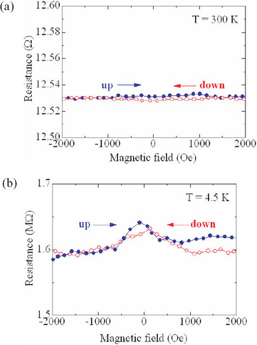
The ratio of MR is defined by ΔR/R0, where R0 is the resistance in the saturation region. At 4.5 K, ΔR/R0 is found to be about 0.7--1.8%. This value agrees with the previous report on the MR of SWNTs [Citation12]. To increase ΔR/R0, effective spin injection from the ferromagnetic electrode to the SWNTs, and spin-coherent transport in SWNTs should be realized. For spin injection, improvement in the Co/SWNT interface quality is necessary. For spin-coherent transport, the growth of high-quality SWNTs and the reduction of L between the electrodes are the most important factors. It is also interesting that the dependence of ΔR/R0 on L can be used to clarify the spin diffusion length of SWNTs.
Summary
We have directly synthesized SWNTs from a Co catalyst on a Mo thin film in FET devices by ACCVD. We investigated the structural properties by SEM, AFM, Raman spectroscopy, and measured the temperature and magnetic field dependence of the magnetic and transport characteristics. Clear MR peaks with ΔR/R0 of up to 1.8% were observed at 4.5 K. This result can be attributed to the spin-dependent transport in SWNT FETs fabricated by direct synthesis.
Acknowledgments
This work is supported in part by the Grant-in-Aid for Scientific Research (grant no. 20048001) from the Ministry of Education, Culture, Sports, Science and Technology (MEXT), Japan. A part of this work was conducted in Kyoto-Advanced Nanotechnology Network, supported by ‘Nanotechnology Network’ of the MEXT, Japan.
References
- BachtoldAFuhrerM SPlyasunovSForeroMAndersonE HZettlAMcEuenP L 2000Phys. Rev. Lett.846082 http://dx.doi.org/10.1103/PhysRevLett.84.6082
- YaoZKaneC LDekkerC 2000Phys. Rev. Lett.842936 http://dx.doi.org/10.1103/PhysRevLett.84.2941
- DresselhausMDresselhausGAvourisPh 2001Carbon Nanotubes: Synthesis, Structure, Properties and Applications Berlin Springer
- TsukagoshiKAlphenaarB WAgoH 1999Nature401572 http://dx.doi.org/10.1038/44108
- HuangSWoodsonMSmalleyRLiuJ 2004Nano Lett.41025 http://dx.doi.org/10.1021/nl049691d
- TsukagoshiKAlphenaarB W 2000Superlatt. Microstruct.27565 http://dx.doi.org/10.1006/spmi.2000.0885
- InamiN 2008 Characterization of carbon nanotube field effect transistor fabricated by direct synthesis method PhD Thesis Japan Advanced Institute of Science and Technology
- JulliereM 1975Phys. Lett.A 54225 http://dx.doi.org/10.1016/0375-9601(75)90174-7
- SahooSKontosTFurerJHoffmannCGraberMCottetASchonenbergerC 2005Nat. Phys.199 http://dx.doi.org/10.1038/nphys149
- NagabhiravaBBansalTSumanasekeraG UAlphenaarB W 2006Appl. Phys. Lett.88023503 http://dx.doi.org/10.1063/1.2164367
- InamiNMohamedM AShikohEFujiwaraA 2007Sci. Technol. Adv. Mater.8292http://dx.doi.org/10.1016/j.stam.2007.02.009
- SagnesMRaquetBLassagneBBrotoJ MFlahautELaurentCOndarcuhuTCarcenacFVieuC 2003Chem. Phys. Lett.372733http://dx.doi.org/10.1016/S0009-2614(03)00488-3