Abstract
Zinc sulfide nanoparticles with average grain sizes ranging from 3 to 12 nm were prepared by arrested chemical preparation, followed by suitable thermal processing. The size of the grains was determined by x-ray line broadening. Dc measurement was performed on compacts of nanoparticles using a Keithley electrometer in the temperature range of 313–423 K. The dc conductivity, σdc, of our samples is much higher than that of ZnS single crystals; σdc increases with a decrease in the grain size.
Introduction
The electrical properties of consolidated nanoparticles of semiconductors show a large deviation from those of their single-crystalline or bulk polycrystalline counterparts [Citation1–8]. These variations in electrical properties are a result of band structure modification, the quantum confinement of charge carriers and the predominant contribution of the largely defective and strained grain boundaries in nanostructured materials [Citation1–13]. For example, for undoped semiconductor nanoparticles, a decrease in conductivity is expected owing to the narrowing of valence and conduction bands resulting in an increase in forbidden energy gap [Citation9]. However, in semiconductor nanoparticles, lattice defects may form acceptor- or donor-like levels in the forbidden energy gap, which can act as trapping centers for charge carriers and which may affect the electrical response of a sample [Citation9, Citation10]. Merchant et al [Citation14] reported the presence of a pseudo-one-dimensional energy band in the forbidden energy gap of ZnS single crystals, which leads to significant changes in the electrical properties of the crystals. However, studies of the electrical properties of nanostructured ZnS are very limited.
In this paper, we discuss the variation in the dc conductivity of consolidated ZnS nanoparticles with different average grain sizes, and the effects of grain boundaries and triple junctions on the dc electrical properties of consolidated samples of nanostructured ZnS.
Experimental
Zinc sulfide nanoparticles were prepared by arrested precipitation using zinc chloride and sodium sulfide as starting materials, and EDTA as stabilizer. All the chemicals used were of E Merck GR grade and all the solutions were freshly prepared before each experiment. The prepared ZnS nanoparticles were separated and washed repeatedly using an ultrasonic disintegrator to remove adsorbed ions. The particles were finally dried at about 370 K. ZnS nanoparticles having different average grain sizes were then produced by annealing the sample in nitrogen atmosphere.
For electrical measurement, the nanoparticle samples were consolidated in the form of cylindrical compacts having a diameter of 13 mm and a thickness of about 1 mm by applying a uniaxial pressure of 0.3 GPa for 2 min using a hydraulic press. All the samples were consolidated under the same conditions. A mixture of colloidal silver and aluminum in suitable proportion was used as electrode. This colloidal mixture was carefully applied on both faces of the pellets to serve as electrodes.
Dc electrical measurement was carried out in an evacuated dielectric cell using a Keithley Model 617 electrometer. Dc electrical resistance was measured in the V/I mode while applying a voltage of 5 V across the samples from a constant-voltage source using the Keithley electrometer. The resistance of the samples was measured at different temperatures between 313 and 423 K keeping each temperature constant within ±1 K. The maximum temperature of measurement was kept below 425 K to prevent the grain growth of the samples and to ensure that the readings correspond to grains of the same average size. The x-ray diffraction (XRD) pattern of each sample after electrical measurement showed no grain growth.
Results and discussion
The XRD patterns of the samples were recorded and the average sizes of the ZnS nanoparticles were determined from x-ray line broadening using Scherrer's equation [Citation15]. Sample codes together with the annealing temperatures and average grain sizes are given in table 1.
Sample codes, annealing temperatures and grain sizes of nanostructured ZnS.
Figure shows the variation in the dc conductivity, σdc, of ZnS nanoparticles with different average grain sizes in the temperature range of 313–423 K. The σdc of the sample Z1 with an average grain size of 3 nm varied from 4.05×10⁻⁷ Ω−1 cm−1 at 313 K to 7.96×10⁻⁶ Ω−1 cm−1 at 423 K, whereas that of the sample Z3 with a grain size of 12 nm was found to increase from 7.79×10⁻⁸ Ω−1 cm−1 at 313 K to 2.36×10⁻⁶ Ω−1 cm−1 at 423 K. The σdc of the sample Z2 with an average grain size of 5 nm was between those of Z1 and Z3. Note that the nature of the variation in σdc with temperature is very similar for samples of different average grain sizes. The σdc of ZnS nanoparticles with an average grain size of 8 nm was reported as 3.24×10⁻⁸ Ω−1 cm−1 at 323 K, which increased to 3.37×10⁻⁷ Ω−1 cm−1 at 423 K [Citation16]. Zinc sulfide nanoparticles with different average grain sizes showed σdc values much higher than that of bulk ZnS, which is reported to be on the order of 10−13 Ω−1 cm−1 [Citation17].
Figure 1 Variation in σdc with temperature for ZnS nanoparticles with average grain sizes of 3, 5 and 12 nm.
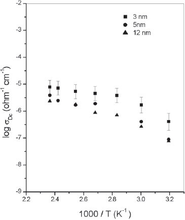
The increase in the electrical conductivity of consolidated nanoparticles compared with that of their single-crystalline or polycrystalline counterparts has also been reported for semiconductors such as ZnO, CdS, ZnS and NiO [Citation3–6, Citation11–13, Citation16, Citation18, Citation19]. In this study, the σdc of the samples of consolidated ZnS nanoparticles is found to be five to seven orders of magnitude higher than that of ZnS single crystals [Citation17] and σdc of the pellets of 5 nm grain size closely agrees with the reported σdc of ZnS pellets of 8 nm grain size [Citation16].
The observed dc electrical properties of nanostructured ZnS can be understood within the established framework of electrical transport in polycrystalline semiconductors that have potential barriers at grain boundaries. A grain boundary potential barrier always exists in polycrystalline semiconductors because the chemical potential of a grain boundary region is shifted from the bulk value owing to the lack of perfect periodicity. Pike et al explained that, in polycrystalline semiconductors, the electrical properties are often predominated by a double depletion layer that forms around grain boundaries [Citation20, Citation21]. The electrical properties of polycrystalline silicon films [Citation21, Citation22] have been interpreted in terms of the grain boundary trapping theory assuming the presence of a large amount of trapping states at the grain boundary, which are capable of capturing free carriers so that they become charged [Citation21]. These charged states create potential barriers at grain boundaries. In nanocrystalline materials, grain boundaries occupy a large fraction of the volume and the properties of nanocrystalline materials are predominated by those of grain boundaries [Citation1, Citation5]. Owing to the grain boundary potential barrier, an energy barrier is generated between two adjacent grains.
According to Seager and Castner [Citation23], there are two distinct mechanisms whereby an electron or a hole incident to a potential barrier can reach the other side: quantum mechanical tunneling and barrier emission. Snejar and Jerhot [Citation24] described a phenomenological model for electrical conductivity in polycrystalline semiconductors by assuming that an isotype heterojunction with a certain interface state density exists at the grain-intergrain interface. According to Snejar and Jerhot [Citation24], thermionic emission is one of the major charge transfer mechanisms across grain boundary barriers in polycrystalline semiconductors. Earlier studies have shown that if the conductivity of a material exhibits Arrhenius behavior, thermionic emission is one of the prominent electrical transport mechanisms [Citation22]. From figure , it is found that all the three ZnS nanoparticle samples exhibit an approximate Arrhenius-type temperature dependence of σdc. It is reasonable to assume that the thermionic emission of charge carriers over a barrier is the major electrical transport mechanism in ZnS nanoparticles.
According to Setto's theory [Citation22], the current across a grain boundary due to thermionic emission results from carriers possessing sufficiently high energy to surmount the potential barrier at the grain boundary. Pike and Seager [Citation20] presented a model suitable for describing the electrical transport properties of grain boundaries when thermionic emission is the only important conduction mechanism. According to this model, the grain boundary conduction is mainly controlled by the energetic distribution of defect states at the interface between space charge regions. Grain boundary studies of Si bicrystals [Citation21] also showed that thermionic emission is the major conductivity mechanism in these crystals. For Si bicrystals, the grain boundary barrier decreases owing to the filling of charge carriers in trap states, which are delocalized levels between the valence and conduction bands. Merchant and Elbaum [Citation14] reported the presence of a pseudo-one-dimensional energy level in the forbidden energy gap of ZnS single crystals. The presence of a pseudo-one-dimensional energy level produces large anisotropies in the dc electrical properties of ZnS single crystals. In nanocrystalline materials, the trap states also form acceptor- or donor-like levels or states in the forbidden gap [Citation9]. The surface states present between the valence and conduction bands can be broadly divided into deep and shallow traps states [Citation9]. Blatter and Greuter [Citation25] explained the role of deep and shallow trap states in carrier transport through grain boundaries in semiconductors in detail. Deep trap states are essentially localized in space and lie deep at the band edge, whereas shallow trap states lie within 3–5 meV of the corresponding band edge. As grain size decreases, the shallow trap state responds to a small size before deep traps [Citation9]. That is, deep trap states are so deep within the gap that trapped charge carriers cannot be thermally ionized easily [Citation9]. Therefore, for nanoparticles of ZnS, it can be assumed that when temperature increases, the possibility of more charge carriers being trapped in shallow trap states increases so that the barrier height of the grain boundary decreases and the thermionic emission of the charge carriers from one grain to another becomes easier, and then increases σdc.
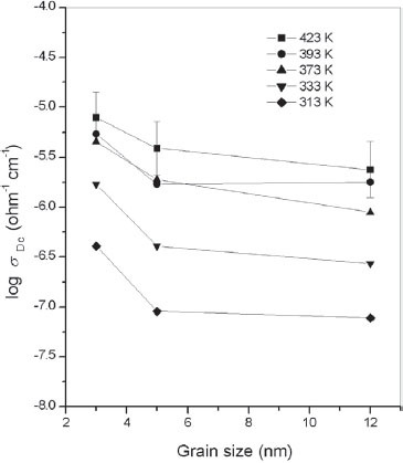
The variation in σdc, with grain size is shown in figure . It can be observed that there is a clear decrease in σdc with an increase in grain size. Nan et al [Citation18] have explained the grain-size-dependent electrical properties of nanocrystalline ZnO on the basis of the potential barrier formed at grain boundaries, which is a consequence of electron trapping in the surface states. This grain boundary potential barrier extends over a length corresponding to the Debye screening length [Citation18]. When the grain size becomes comparable to the Debye screening length, the grain interior becomes entirely depleted of electrons due to the trapping of electrons at the interface or in the surface states. In fine-grained nanocrystalline materials, the carriers are effectively captured in the traps at grain boundaries. However, in larger samples, the number of traps per volume may be smaller, and hence the number of charge carriers trapped at the interface will also be smaller. It was also reported in the case of semiconductors that, when grain size decreases, there is a greater chance for charge carriers to escape to the surface [Citation4, Citation26]. In nanostructured materials, because a large portion of a material resides in the interfacial region, the structure and volume fraction of the interfacial region largely determine electrical transport properties [Citation1–10]. The interfacial region of nanostructured materials is composed of grain boundaries and triple junctions. Triple junctions, which are the intersection lines of three or more adjoining grains, are a very important component of the interface along with grain boundaries [Citation5, Citation27]. Bollman [Citation28, Citation29] reported that triple junctions in nanostructured materials should be viewed as line defects, which are analogous to dislocations. The interfacial region of nanostructured materials can be pictured as constituting a potential barrier for charge carriers with triple junctions corresponding to the maxima of the barrier [Citation27–30]. The observed variation in σdc, with grain size in nanostructured NiO was explained on the basis of the combined effects of grain boundaries and triple junctions present in nanostructured materials [Citation19]. In the following semiquantitative analysis, an explanation of the observed variation in the dc conductivity of pellets of ZnS nanoparticles with an average grain size is presented on the basis of the variation in the volume fractions of grain boundaries (Vgb) and triple junctions with an average grain size.
Figure 2 Variation of σdc with grain size.
According to Palumbo et al [Citation27], the grains of nanostructured materials are assumed to have a regular tetrakaidecahedron shape with hexagonal faces representing grain boundaries and edges corresponding to triple junctions for calculating interfacial volume fraction. For nanostructured samples of ZnS, an estimation of the volume fractions of the total interfacial region (Vif), grain boundaries (Vgb) and triple junctions (Vtj) was carried out in this study by assuming that grains have a regular fourteen-sided tetrakaidecahedron shape. The volume fractions are given by
(1)
(2)
(3)
where d is the average grain size, which is assumed to be the maximum diameter of an inscribed sphere, and D/2 is the thickness of the interfacial region (outer skin of the tetrakaidecahedron) [Citation5, Citation27]. For all calculations, D/2 is assumed as 0.5 nm, which is realistic in the size range of the samples used in this study [Citation27].
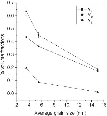
Figure shows the variations in Vif, Vgb and Vtj for ZnS nanoparticles having different average grain sizes. The volume fraction of the total interfacial region, Vif, is maximum for Z1, with a minimum average grain size of 3 nm and the interfacial volume is found to decrease with an increase in grain size. The volume fractions of the grain boundaries and triple junctions are also higher for smaller particles than for larger particles. That is, as grain size decreases, the volume fractions of the interfacial region as well as of grain boundaries and triple junctions increase so that the possibility of more charge carriers being trapped at shallow levels of the grain boundary increases. Hence, the barrier height of grain boundaries decreases so that the thermionic emission of the charge carriers from one grain to another becomes easier, which then results in an increase in σdc with a decrease in grain size for nanostructured ZnS samples.
Figure 3 Variations in calculated volume fractions of total interfacial region (Vif), grain boundaries (Vgb) and triple junctions (Vtj) with average grain size for ZnS nanoparticles.
Conclusion
The σdc of nanostructured ZnS samples having different average grain sizes of 3, 5 and 12 nm was measured in the temperature range 313–423 K. The σdc of all the samples is five to eight orders of magnitude higher than that of single crystals. This increase in σdc is explained on the basis of the thermionic emission of charge carriers from the trapped states of a grain boundary potential barrier. The observed variation in σdc with average grain size is explained by considering the combined effects of grain boundaries and triple junctions on electrical transport in nanostructured ZnS.
References
- MathurG N 2002 Prog. Cryst. Growth Charact. Mater. 45 167 http://dx.doi.org/10.1016/S0960-8974(02)00044-X
- NalwaH S 2000 Handbook of Nanostructured Materials and Nanotechnology USA Academic
- KhadarM AThomasB 1995 Phys. Status Solidi A 150 75
- ThomasBKhadarM A 1995 Pramana J. Phys. 45 431 http://dx.doi.org/10.1007/BF02875177
- SuryanarayanaC 1994 Bull. Mater. Sci. 17 302
- BijuVKhadarM A 2001 Mater. Sci. Eng. A 304–306 814 http://dx.doi.org/10.1016/S0921-5093(00)01581-1
- SchoonmanJ 2000 Solid State Ion. 135 5 http://dx.doi.org/10.1016/S0167-2738(00)00324-6
- PonpandianNNarayanaswamyA 2002 J. Appl. Phys. 92 2770 http://dx.doi.org/10.1063/1.1498883
- BrusL 1986 J. Phys. Chem. 90 2555 http://dx.doi.org/10.1021/j100403a003
- BrusL 1998 J. Phys. Chem. Solids 59 459 http://dx.doi.org/10.1016/S0022-3697(97)00201-1
- JoseJKhadarM A 1999 Nanostruct. Mater. 11 1091 http://dx.doi.org/10.1016/S0965-9773(99)00399-2
- JoseJKhadarM A 2001 Acta Mater. 49 729 http://dx.doi.org/10.1016/S1359-6454(00)00369-4
- JoseJKhadarM A 2001 Mater. Sci. Eng. A 810 304
- MerchantPElbaumC 1978 Solid State Commun. 26 73 http://dx.doi.org/10.1016/0038-1098(78)90499-4
- TaylorA 1961 X-ray Metallography New York Wiley p 674
- KhadarM AThomasB 1998 Nanostruct. Mater. 10 593 http://dx.doi.org/10.1016/S0965-9773(98)00100-7
- BirringuierE 1997 Phil. Mag. B 75 209 http://dx.doi.org/10.1080/13642819708202310
- NanC-WSchopeTHoltenSKleimHBirringerR 1999 J. Appl. Phys. 85 7735 http://dx.doi.org/10.1063/1.370578
- BijuVKhadarM A 2001 Mater. Res. Bull. 36 21 http://dx.doi.org/10.1016/S0025-5408(01)00488-3
- PikeG ESeagerC H 1979 J. Appl. Phys. 50 3414 http://dx.doi.org/10.1063/1.326334
- SeagerC HPikeG E 1979 Appl. Phys. Lett. 35 709 http://dx.doi.org/10.1063/1.91264
- SettoY W J 1975 J. Appl. Phys. 46 5247 http://dx.doi.org/10.1063/1.321593
- SeagerC HCastnerT G 1978 J. Appl. Phys. 49 3879 http://dx.doi.org/10.1063/1.325394
- SnejdarVJerhotJ 1976 Thin Solid Films 37 303 http://dx.doi.org/10.1016/0040-6090(76)90600-3
- BlatterGGreuterF 1986 Phys. Rev. B 33 3952 http://dx.doi.org/10.1103/PhysRevB.33.3952
- SlenderJ A 1987 Chem. Rev. 87 877 http://dx.doi.org/10.1021/cr00081a002
- PalumboGThorpeS JAustK T 1990 Scr. Metall. Mater. 24 1347 http://dx.doi.org/10.1016/0956-716X(90)90354-J
- BollmanW 1984 Philos. Mag. A 49 73 http://dx.doi.org/10.1080/01418618408233430
- BollmanW 1989 Mater. Sci. Eng. A 113 129 http://dx.doi.org/10.1016/0921-5093(89)90299-2
- MeilikhovE ZFarzetdinovaM 1998 Physica E 3 190 http://dx.doi.org/10.1016/S1386-9477(98)00235-5