Abstract
We experimentally demonstrate the effect of the rapid thermal annealing (RTA) in nitrogen flow on photoluminescence (PL) of SiO2 films implanted by different doses of Si+ ions. Room-temperature PL from 400-nm-thick SiO2 films implanted to a dose of 3×1016 cm−2 shifted from 2.1 to 1.7 eV upon increasing RTA temperature (950–1150 °C) and duration (5–20 s). The reported approach of implanting silicon into SiO2 films followed by RTA may be effective for tuning Si-based photonic devices.
Introduction
Given the advantages of Si technology in electronic integrated circuits and its potential applications in photonics and optoelectronics, silicon nanocrystals embedded in SiO2 have attracted much attention [Citation1]. Room-temperature visible photoluminescence (PL) was first observed from porous silicon, but many practical problems have been encountered in exploiting this property [Citation2, Citation3]. Plasma-enhanced chemical vapor deposition [Citation4], evaporation and the termination of the glass-melt reactions [Citation5] have been used to produce silicon nanocrystals emitting visible light, but none of those techniques was found suitable for manufacturing integrated devices. Silicon implantation into SiO2 film grown on crystalline Si, followed by annealing, is another method of fabricating Si-based luminescent structures. Many research groups have observed emission bands between 1.5 and 2.0 eV after implanting Si+ into SiO2 films and conventional annealing above 1000 °C in vacuum, Ar or N2 [Citation6–11]. However, the implantation doses were relatively high (>1017 cm−2) and the annealing process took several hours. Spectral shift of PL upon short annealing (seconds) has not been studied much.
In this study, we applied rapid thermal annealing (RTA) to 400-nm-thick Si+-implanted SiO2 films. Increasing RTA temperature (950–1150 °C) or duration (5–20 s) shifts the PL maximum from 2.1 to 1.7 eV. This approach can reduce the doses of Si+ implantation and shorten the processing time—entire RTA process takes less than 30 min. We studied the effect of different treatment parameters on the PL shift. The shift increased with the increasing concentration of silicon ions in SiO2, with RTA temperature and duration. Fourier transform infrared (FTIR) transmittance measurements demonstrated minor effects of Si–O–H, Si–H or C–H groups on PL. Finally, we show data suggesting that the PL mechanism is the same for RTA and conventional annealing of SiO2 films, namely precipitated silicon nanocrystals [Citation6–12].
Experimental procedure
Samples were prepared by implanting Si+ into a 400-nm-thick SiO2 layer thermally grown on (100)-oriented p-doped Si substrates. The doses of the implanted Si+ were 4×10¹⁵, 1×10¹⁶ and 3×1016 cm−2. During the implantation, the samples were kept at liquid nitrogen temperature. Acceleration energy of 160 keV resulted in the estimated implanted depth of 250 nm with the standard deviation of ±60 nm. The samples were subjected to RTA in N2 flow. Gas pressure of 50 mbar was applied to the furnace entrance; heating rate was ∼100 °C s−1 and cooling rate was ∼100 °C min−1. The annealed films were etched with a 10% aqueous HF solution to reduce the SiO2 thickness to 260, 160 and 100 nm. The average SiO2 layer thickness was determined using atomic force microscopy.
Luminescence was excited with a He–Cd laser (3.8 eV, 5 mW) and detected using a monochromator, cooled photomultiplier tube and lock-in detection which improved the signal-to-noise ratio. No PL could be detected from 3×1016 cm−2 Si+-implanted SiO2 films without annealing.
Hydrogen-related species in the oxide films were studied by FTIR transmittance. Spectra were recorded at room temperature in N2 atmosphere with a 2 cm−1 resolution and 200-scan averaging.
Results and discussion
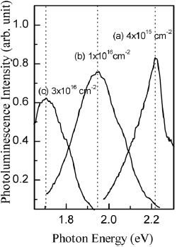
Figure demonstrates the effect of Si+ dose (4×10¹⁵, 1×10¹⁶ or 3×1016 cm−2) on PL spectra from SiO2 films subjected to RTA at 1150 °C for 20 s. A shift from ∼2.2 eV to 1.7 eV with increasing dose is observed, thus revealing that the Si+ dose determines the PL peak position. PL intensity decreases with the dose, but the decrease is minor.
Figure 1 PL spectra of 400-nm-thick wet SiO2 films implanted by Si+ ions to doses of (a) 4×1015 cm−2, (b) 1×1016 cm−2, and (c) 3×1016 cm−2 after dry-N2RTA for 20 s at 1150 °C.
Curve (a) of figure shows PL spectrum of the 3×1016 cm−2 Si+-implanted SiO2 film after RTA in dry N2 at 1150 °C for 20 s. When the thickness of SiO2 layer was reduced by etching from 400 nm to 260 nm (b) and 160 nm (c), PL maximum shifted from 1.7 to 1.6 eV and the line width has reduced. No PL could be detected when SiO2 was etched down to 100 nm. These results confirm our estimate of the implantation depth (250 ± 60 nm). They also suggest that larger implanted Si+ density results in bigger Si clusters and thus and lower-energy PL.
Figure 2 PL spectra of 400-nm-thick 3×1016 cm−2 Si+-implanted SiO2 film after dry-N2RTA at 1150 °C for 20 s, without (a) and with (b, c) subsequent HF etching. The etching reduced the SiO2 thickness from 400 nm (a) to 260 nm (b), and 160 nm (c).

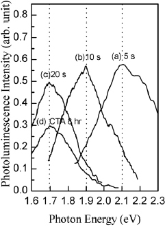
We have further analyzed the effects of the temperature and duration of RTA on the PL shift. As the temperature of isochronal (20 s) dry-N2 RTA is increased from 950 to 1150 °C, luminescence shifts from 2.1 to 1.7 eV, as shown in figure . Similar shift is observed when the duration of isothermal (1150 °C) RTA is increased from 5 to 20 s (figure ). Figure also shows PL spectrum of the 1×1017 cm−2 Si+-implanted SiO2 film after 8 h of conventional, slow annealing (curve d). Slow annealing also shifts PL peak to 1.7 eV, but PL intensity is reduced as compared to RTA. Similar PL peak at 1.7 eV was observed by Fernandez et al in the 800-nm-thick Si+-implanted (150 keV, 1×1017 cm−2) SiO2 films after slow annealing at 1100 °C for 8 h [Citation10] and by Mutti et al in 430-nm-thick Si+-implanted (160 keV, 3×1017 cm−2) SiO2 films annealed at 1000 °C for 5 h [Citation7].
Figure 3 PL spectra of 400-nm-thick 3×1016 cm−2 Si+-implanted SiO2 film after dry-N2RTA for 20 s at 950 °C (a), 1050 °C (b), and 1150 °C (c).
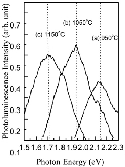
Figure 4 PL spectra of 400-nm-thick 3×1016 cm−2 Si+-implanted SiO2 film after dry-N2RTA at 1150 °C for 5 s (a), 10 s (b), and 20 s (c). Curve (d) corresponds to the Si+ dose of 1×1017 cm−2 and slow annealing in dry N2 at 1150 °C for 8 h.
We have analyzed the effect of implantation and annealing on the density of Si–Hx (x=1,3) and Si–O–H bonds via FTIR absorption at ∼2100 cm−1 (figure ) and ∼3750 cm−1 (figures and ), respectively [Citation13, Citation14–16]. We could not detect absorption peaks at ∼1450 or ∼2900 cm−1 corresponding to C–Hx bonds [Citation14, Citation17]. Figure reveals that Si–Hx absorption depends on the SiO2 thickness; this absorption is weak for the studied 400 nm films and it is not affected by Si+ implantation and dry-N2 RTA. Similar conclusion can be made regarding the Si–O–H bonds (curves a, d, e in figure ). In order to produce Si–O–H bonds, we have annealed 400 nm Si+ implanted SiO2 films in wet nitrogen. Figures and reveal that such annealing does induce Si–O–H absorption peaks and their intensity is stronger for higher Si+ implantation doses. Luminescence spectra from those samples (inset in figure ) showed intensity decrease in wet-N2 annealed samples as compared to SiO2 films annealed in dry N2 [Citation18, Citation19]. The PL peak shift in figure is due to different implantation doses. This intensity decrease suggests that Si–O–H groups are not the origin, but perhaps a quencher of the observed PL; neither Si–O–H nor Si–Hx or C–Hx bonds seem to affect the PL from SiO2 films annealed in dry N2.
Figure 5 FTIR spectra of 100 nm (a), 200 nm (b) and 400 nm thick (c) SiO2 films without Si+ implantation or annealing, and of 400-nm-thick film Si+ implanted to doses of 1×1016 cm−2 (d) and 3×1016 cm−2 (e) after RTA at 1150 °C for 20 s.
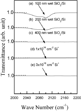
Figure 6 FTIR spectra of 400-nm-thick SiO2 films without implantation or RTA (a), Si+-implanted to doses of 4×1015 cm−2 (b) and 1×1016 cm−2 (c) and subjected to wet-N2 RTA at 1150 °C for 20 s, Si+-implanted to doses of 1×1016 cm−2 (d) and 3×1016 cm−2 (e) and subjected to dry-N2RTA at 1150 °C for 20 s.
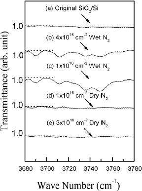
Figure 7 FTIR spectra of 400-nm-thick SiO2 films Si+-implanted to dose of 1×1016 cm−2 and RTA-treated in dry-N2 at 1150 °C for 20 s (a), or Si+-implanted to doses of 1×1016 cm−2 (b) and 4×1015 cm−2 (c) and subjected to wet-N2RTA at 1150 °C for 20 s. The inset shows corresponding PL spectra.

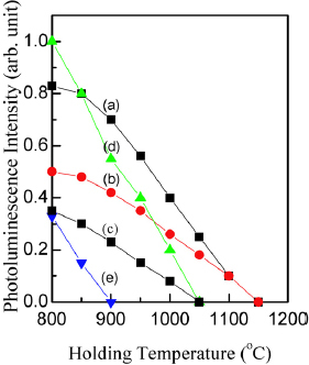
Figure shows the PL peak intensities for temperatures of additional RTA for 10 min in dry N2. It reveals similar annealing behavior for different implantation doses and annealing procedures (rapid or slow annealing), thus suggesting similar mechanism of PL induced at those conditions. Comparison of curves d and e also confirms much weaker PL intensity in Si+ implanted SiO2 annealed in wet nitrogen than annealed in dry nitrogen.
Figure 8 Changes in PL intensity of 400-nm-thick 3×1016 cm−2 Si+-implanted SiO2 film subjected to RTA at 1150 °C for 20 s (a) or slow annealing at 1150 °C for 12 h (b). Curves (c–e) correspond to the lower Si+ dose of 1×1016 cm−2 followed by slow annealing at 1150 °C for 12 h (c) or RTA at 1150 °C for 20 s in dry (d) or wet (e) nitrogen. X-scale is temperature of additional RTA applied to those samples in dry N2 for 10 min at a heating rate of 50 °C s−1.
Conclusions
We have experimentally demonstrated the effect of RTA on the shift of room-temperature photoluminescence in Si+-implanted SiO2 film. The PL shift increases with the Si+ dose, RTA temperature and duration. Infrared absorption suggests that the PL is not related to C–H, Si–H or Si–O–H groups. Comparison of PL between rapid and slow annealing suggests similar origin of PL, namely Si nanocrystals in the oxide matrix [Citation6–11, Citation20]. The PL peak position can be tuned between 1.7 and 2.1 eV by varying RTA temperature (950–1150 °C) and RTA duration (5–20 s); the processing time is significantly shorter for RTA than for conventional annealing. Those attractive features of RTA appear useful for manufacturing of optoelectronic devices.
References
- BrusL 1998 Semiconductors and Semimetals vol 490 New York Academic p 303
- Sabet-DarianiRMcAlpineN SHanemanD 1994 J. Appl. Phys. 75 8008 http://dx.doi.org/10.1063/1.356539
- QinG GLiA PZhangB RLiB 1995 J. Appl. Phys. 78 2006 http://dx.doi.org/10.1063/1.360175
- KakiuchiHOhmiHHaradaMWatanabeHYasutakeK 2007 Sci. Techn. Adv. Mater. 8 137 http://dx.doi.org/10.1016/j.stam.2006.12.006
- KuniyoshiKOzonoKIkedaMSuzukiTKimS GKimW T 2006 Sci. Techn. Adv. Mater. 7 595 http://dx.doi.org/10.1016/j.stam.2006.06.001
- Shimizu-IwayamaTKurumadoNHoleD ETownsendP D 1998 J. Appl. Phys. 83 6018 http://dx.doi.org/10.1063/1.367469
- MuttiPGhislottiGBertoniSBonoldiLCerfoliniG FMedaLGrilliEGuzziM 1995 Appl. Phys. Lett. 66 851 http://dx.doi.org/10.1063/1.113408
- ZhuJ GWhiteC WBudaiJ DWithrowPChenY 1995 J. Appl. Phys. 78 4386 http://dx.doi.org/10.1063/1.359843
- KenyonA JChryssouC EPittC WShimizu-IwayamaTHoleD ESharmaNHumphreysC J 2002 J. Appl. Phys. 91 367 http://dx.doi.org/10.1063/1.1419210
- FernandezB GLopezMGarciaCPerez-RodriguezAMoranteJ RBonafosCCarradaMClaverieA 2002 J. Appl. Phys. 91 798 http://dx.doi.org/10.1063/1.1423768
- ChenT PLinYTseM SFungSDongG 2004 J. Appl. Phys. 95 8481 http://dx.doi.org/10.1063/1.1739282
- AllianGDelerueCLannooM 1993 J. Lumin. 57 239 http://dx.doi.org/10.1016/0022-2313(93)90141-9
- WengY MFanZ NZongX F 1993 Appl. Phys. Lett. 63 168 http://dx.doi.org/10.1063/1.110388
- StesmansAScheerlinckF 1994 J. Appl. Phys. 75 1047 http://dx.doi.org/10.1063/1.356486
- TrukhinA NJansonsJFittingH JBarfelsTSchmidtB 2003 J. Non-Cryst. Solids 331 91 http://dx.doi.org/10.1016/j.jnoncrysol.2003.08.080
- LinG RLinC J 2004 J. Appl. Phys. 95 8484 http://dx.doi.org/10.1063/1.1739283
- ZvanutM EChenT LStahlbushR ESteigerwaltE SBrownG A 1995 J. Appl. Phys. 77 4329 http://dx.doi.org/10.1063/1.359456
- AgarwalMDunhamS T 1995 J. Appl. Phys. 78 5313 http://dx.doi.org/10.1063/1.359708
- ShimH WKimK CSeoY HNahmK SSuhE KLeeH JHwangY G 1997 Appl. Phys. Lett. 70 1757 http://dx.doi.org/10.1063/1.118648
- IwayamaT SHamaTHoleD EBoydI W 2006 Vacuum 81 179 http://dx.doi.org/10.1016/j.vacuum.2006.03.023