Abstract
This work investigates the root causes of streak defects, appearing as narrow, bright bands, on an anodised AA 6063-T6 extrusion using optical and electron microscopies. It was found that the appearance of etched and anodised aluminium alloy is associated with grain boundary grooves, etching steps and surface scallops which are determined by the distributions of grain size and crystallographic orientations. It was also revealed that the bright streaking regions had relatively large grains with a relatively strong texture. Such microstructure resulted in reduced light scattering by grain boundary grooves, surface scallops and etching steps with, consequently, brighter appearance.
Introduction
Surface appearance is an important characteristic of high quality aluminium extrusions, especially for architectural applications in the building and construction industries.Citation1 Surface defects such as streaking are often present on anodised extrusions of 6xxx series alloys,Citation1–Citation3 increasing the fabrication cost of these products. Streaking on the surfaces of anodised extrusions is typically characterised by narrow bands of different contrasts to the neighbouring material. The streak bands may appear darker or lighter, duller or brighter, in colour and tone compared with the surrounding material.Citation2 Streaking often only becomes visible after etching and anodising treatments, rather than in the as extruded condition, making it difficult to identify the original causes of the defect.Citation3
The streak defects can be detected by the naked eye due to their difference in surface gloss in different locations of the extrusions. Given the material and incident light, the surface gloss is dependent on the microtopography of the surface of the material. Smooth surfaces appear glossy while very rough surfaces appear matte. Surface roughness height >200 nm can be detected by the naked eye and therefore influences surface gloss.Citation2 There are generally four typical surface features which can lead to decrease in surface gloss on alkaline etched extrusions, namely etching pits, grain boundary grooves, etching steps and surface defect remains.Citation1–Citation3 Etching pits are surface scallops or cavities formed as a consequence of different etching behaviours between intermetallic particles or inclusions and the aluminium matrix. Grain boundary grooves are groove shaped imperfections along grain boundary regions formed due to preferential attack of grain boundaries. Etching steps are steps between grains of different orientations due to different etching rates. Surface defect remains refer to any surface defects which are generated during the extrusion process and remain after alkaline etching. Streak defects can originate from the distribution of each individual surface feature listed above or from a combination of them.
The aim of this paper is to identify the root causes of streak defects on an anodised AA 6063-T6 extrusion weld and its associated microstructural features in the alloy. The extrusion was initially etched in sodium hydroxide solution and, subsequently, anodised in sulphuric acid solution. Optical and electron microscopies have been conducted on the as anodised extrusion and the alloy after film stripping, reetching and reanodising.
Experimental
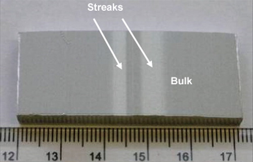
AA 6063-T6 extrusion weld, anodised under industrial conditions, displays streak defects (), with the region along the welding line appearing brighter compared with the bulk surface. Total reflectance of the streaking and bulk regions was measured with an SPECORD 250 spectrophotometer within the wavelength range of 300–800 nm. The surface morphology of the as anodised alloy was examined by optical microscopy and scanning electron microscopy (SEM). Cross-sections of the specimens were prepared through mechanical grinding with 800, 1200 and 4000 grit silicon carbide papers and then examined by SEM.
Figure 1. Optical image of extrusion with streak defects
In order to characterise the microstructure of the alloy substrate immediately beneath the anodic film in the streaking and bulk regions, the anodic film was stripped in 10 wt-% NaOH at 60°C for 2 min, followed by desmutting in 30 vol.-%HNO3 solution for 30 s and then rinsing in deionised water (referred to as film stripped specimen). Before film stripping, the locations of streak defects were marked with dents on the specimen surface. Following film stripping, the microstructure of the alloy substrate in streaking and bulk regions was characterised by SEM. Investigations were performed in the middle of the streak and regions remote from the streak.
With the consideration that the alloy microstructure which caused the streak defects on the as anodised extrusion might have been converted or consumed by the anodising and the subsequent film stripping process, it is essential to examine the alloy microstructure before anodising in regions where streak defects were generated and in regions where streak defects are absent. Since the anodic alumina film is transparent, streak defects, if present, should also be visible after alkaline etching. Therefore, it is practically possible to locate the streaking and bulk regions after alkaline etching. Thus, a selected specimen was mechanically ground with 800, 1200 and 4000 grit silicon carbide papers to remove the anodic film and, subsequently, etched in 5 wt-%NaOH at 60°C for 10 min, followed by desmutting in 30 vol.-%HNO3 solution for 30 s (referred to as reetched specimen). Following careful microstructural characterisation of the reetched specimen, the specimen was then anodised in 2M sulphuric acid at a current density of 1·5 A dm−2 at 20°C for 20 min (referred to as reanodised specimen).
The appearances of the as anodised, reetched and reanodised specimens were recorded using a Canon EOS 550D digital camera under natural lighting condition. For optical microscopy, an Olympus BH-2 microscope, equipped with a Leica DC 200 MTV-3 camera, was used. Polarised light was explored to enhance grain orientation effects in case of necessity. As a complement to optical microscopy, a Veeco interferometer, with ‘Vision 64’ software for data processing, was used to reveal the topography of anodised or alkaline etched surfaces. A Philips XL 30 field emission gun scanning electron microscope, fitted with energy dispersive X-ray facilities, was used for plan and cross-sectional examination of the anodic films and for microstructural characterisation of the alloy substrates. A Zeiss Ultra 55 field emission gun scanning electron microscope, operating at an acceleration voltage of 20 kV, was used for electron backscatter diffraction (EBSD) analysis.
Results
The total reflectance measured within the wavelength range of 300–800 nm () indicates ∼10% more total reflectance in the streak region than the bulk region. shows optical micrographs of the streaking () and bulk () regions on the as anodised extrusion, imaged with polarised light. Grain boundaries appear dark in the images, enabling observation of the distribution of grains in each region. Grains in the streaking region are similar to or slightly larger than those in the bulk region. Interestingly, the contrast between the grains, originating from the difference in surface features between the grains and general surface topography, and related to grain orientations, is less evident in the streaking region than the bulk region, suggesting that etching induced difference in surface topography between grains is less significant in the streaking region than the bulk region. The SEM images of the anodic films () show very similar film morphology in the streaking and bulk regions. The inserts in show typical grain boundary grooves in the streaking and bulk regions.
Figure 2. Total reflectance of streak (top) and bulk (bottom) regions
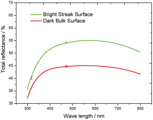
Figure 3. Optical micrographs of anodic film: polarised light was used to enhance grain orientation effect
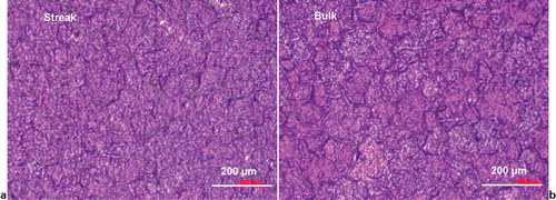
Figure 4. Backscattered electron micrographs of anodic film: insets show typical grain boundary grooves at increased magnifications
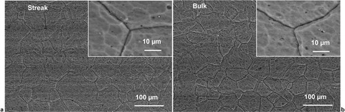
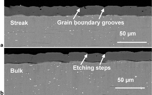
shows typical backscattered electron micrographs of the cross-sections of the as anodised anodic film attached to the alloy substrate in the streaking () and bulk () regions, revealing waved profiles of film surface and film/alloy interface in both regions. Despite the waved profile, the thickness of the anodic film is similar across the alloy surface in both regions, suggesting that such a surface profile did not originate from the anodising process but from the treatment before anodising, i.e. alkaline etching. Scrutiny of reveals a few shallow and narrow valleys in the anodic film, with typical features indicated by the arrows. Between every two valleys is a relatively flat area of tens of micrometres in dimension, which are consistent with the dimensions of grains revealed in and . Therefore, it is believed that such valleys correspond to the locations of grain boundary grooves formed during alkaline etching and the regions between them correspond to grain bodies. Further, steps between the flat regions with dimensions consistent with that of grains were frequently observed in the bulk region, as indicated by the arrows in . Such steps are generated by etching as a consequence of different etching rates between the grains of different grain orientations.
Figure 5. Backscattered electron micrographs of cross-section of anodic film attached to alloy substrate
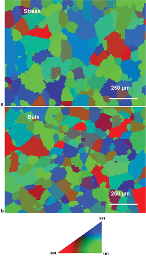
The EBSD analyses were performed on an area of 925×1228 μm in both the streaking and bulk regions. The EBSD maps of the streaking and bulk regions are shown in respectively, where grains of different orientations are displayed in different colours. The relationship between grain orientation and grain colour is displayed in the unit triangle. It is evident that the grain orientations (the grain colours) are slightly more random for the bulk region than the streaking region. Further, grain statistics of the streaking and bulk regions indicate that the average grain size in the streaking region (99·71 μm) is ∼16% larger than that in the bulk region (86·04 μm).
Figure 6. Map (EBSD) of alloy substrate after film stripping
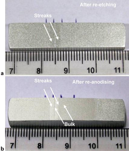
shows an optical image of the specimen after film stripping, mechanical polishing and alkaline etching, revealing two streaks (as indicated by the arrows) with appearances different from that of surrounding alloy surface, near the regions where the streak defects were present on the as anodised extrusion. shows the same specimen after anodising, clearly revealing two streaks which are separated by a narrow region of appearance consistent with that of the bulk region. Apparently, the streak defects shown in are comparable with those shown in , although their locations and dimensions have changed. Therefore, the microstructure causing the streak defects shown in should be similar to that causing the streak defects shown in . Thus, the microstructural factors responsible for the original streak defects can be understood by studying the microstructure of the alloy in the streaking and bulk regions displayed in .
Figure 7. Optical images of alloy after a reetching and b reanodising
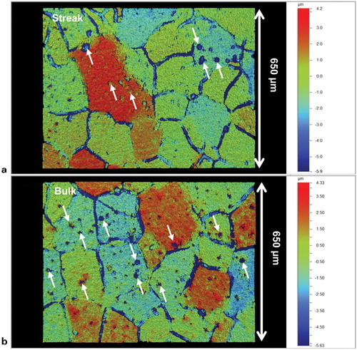
The optical micrographs of the streaking and bulk regions of the as etched specimen are shown in respectively. Generally, grains in the streaking region are larger than the bulk region. Additionally, more dark spots of 10–20 μm diameter are revealed in grains in the bulk region relative to the streaking region. The surface morphology of the as etched specimen in the streaking and bulk regions is compared in , revealing the narrow band of the bulk region, as indicated by the dashed line, between the two streaking regions. , imaged with the interferometry, shows typical topography of the streaking and bulk regions. Different colours in represent different surface heights, with the correlations indicated by the colour bar. Evidently, grain colours are relatively more uniform in the streak region () than the bulk region (), suggesting less significant etching steps in the streak region. Further, surface features of micrometre dimensions, as indicated by the arrows, are more frequently revealed in grains in bulk region than streak region, which is consistent with the distribution of dark spots in the optical micrographs.
Figure 8. Optical micrographs of alloy substrate after film stripping and alkaline etching
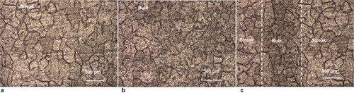
Figure 9. Interferometry topography of alkaline etched specimen
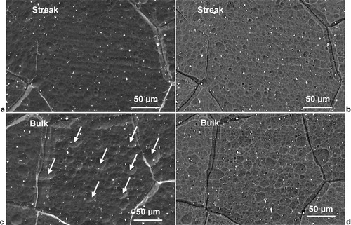
shows SEM images taken from the streaking region () and bulk region (), focusing on relatively fine features in grain interiors. As shown in , scalloped regions of micrometre dimensions are evident for both samples. However, there are more relatively large scalloped regions in the bulk region than the streak region, as indicated by the arrows in . The distribution of the scalloped regions is consistent with that of surface features of micrometre dimensions revealed in and . Such surface scallops resulted from the presence of iron containing particles (Al–Fe–Si in this alloy), which have a higher electrochemical potential than the aluminium matrix during alkaline etching, thereby acting as local cathodic reaction sites and stimulating anodic dissolution of surrounding aluminium matrix.Citation4,Citation5 shows the distribution of Al–Fe–Si particles, revealed as bright particles in the backscattered images, in the streaking and bulk regions. It is evident that the distribution of iron containing particles is similar in streaking and bulk regions.
Figure 10. Images (SEM) of alloy substrate: a, b streak and c, d bulk regions. a, c are secondary electron images and b, d are corresponding backscattered electron images
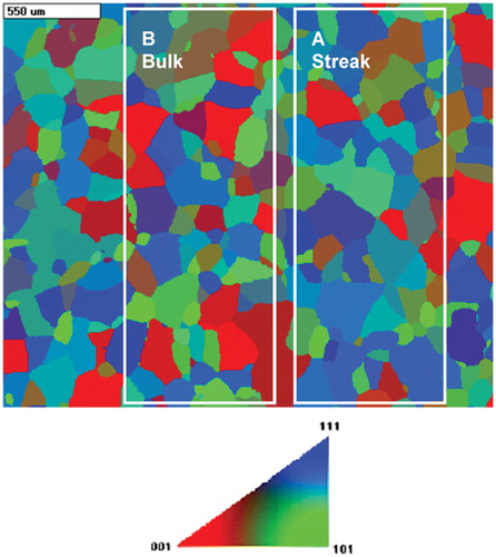
The EBSD analysis was also performed on the as etched specimen, as shown in . Grains of different orientations are revealed in different colours. The relationship between grain orientation and grain colour is displayed in the unit triangle. The framed areas A and B (680×2260 μm in size) in correspond to the streaking and bulk regions respectively. Evidently, the grain orientations (the grain colours) are relatively random in the bulk region, contrasting to the streaking region which has a relatively strong texture. Grain statistics of the streaking and bulk regions indicate that the average grain size in the streaking region (356·38 μm) is ∼18% larger than that in the bulk region (301·44 μm), in agreement with the result shown in .
Figure 11. Map (EBSD) of as etched sample in streak/bulk interface region. Framed area A represents typical streak region and framed area B represents typical bulk region
Discussion
One of the major differences in the microstructure between the streaking regions and the bulk alloy is that grains are larger in the streaking regions than the bulk alloy. This was repeatedly observed on the as anodised extrusion, the film stripped specimen and the reetched specimen, suggesting that grain size is one of the main reasons causing the streak defects. The SEM analyses () indicated that grain boundary grooves have been formed during alkaline etching in both the streaking and bulk regions due to preferential etching of grain boundaries. For a specific area, the population density of the grain boundary grooves decreases with the increase in grain size. Thus, the streaking region contains reduced grain boundary grooves compared with the bulk region. Reduced grain boundary grooves mean reduced scattering of light, leading to a relatively bright appearance in the streaking region.
Etching steps are more significant in the bulk region compared with the streaking region on the as anodised ( and ) and reetched specimens (). The formation of etching steps is associated with different etching behaviours of different grains, which is grain orientation dependent.Citation6,Citation7 Thus, the more random are the grain orientations of the alloy substrate, the more etching steps are likely to be formed after alkaline etching. The relatively strongly textured microstructure in the streaking region resulted in reduced etching steps between grains compared with the bulk alloy. Reduced etching steps mean reduced scattering of light, consequently leading to a relatively bright appearance in the streaking region.
Further, large surface scallops with diameters of 10–20 μm, were more frequently observed in the bulk region compared with the streaking region. Surface scallops usually originate from different chemical behaviours of coarse intermetallic particles and the aluminium matrix during alkaline etching. The SEM analyses () indicated that the distributions of Al–Fe–Si particles are similar in the bulk and streaking regions. Therefore, like the formation of etching steps, the different morphologies of the surface scallops might be also associated with the grain orientations. Reduced surface scallops mean reduced scattering of light, consequently leading to a relatively bright appearance in the streaking region, as above.
It is interesting to note that grain size shown in , in both streak and bulk regions, is generally larger than that shown in . However, the difference of grain size between the streak and the bulk regions in each case is evident. Additionally, it was found that the widths of the streaking region became narrower when a significant thickness of the alloy was removed by film stripping and reetching (), suggesting that it is possible to eliminate the streaks from the profile by increasing the time of alkaline etching. However, it is practically not allowed in the industry to significantly increase etching time, e.g. from 10 to 20 min, since this will result in extra reduction in the extrusion thickness by 57–81 μm on each face, with an etching rate of 95–135 nm s−1.Citation8 Therefore, remedies to this issue have to be sought from other aspects. Improving the extrusion parameters can be helpful. However, it is sometimes unavoidable to have non-uniform microstructures across the extrusion surface, especially for complex profiles. Thus, with the consideration that the streak defects are caused by surface features arising mainly from alkaline etching process, it is believed that to replace the alkaline etching process with other surface pretreatments, for instance acidic etching, may be a feasible solution.
Conclusions
It is found that the appearance of etched and anodised aluminium alloy is associated with grain boundary grooves, etching steps and surface scallops which are determined by the distributions of grain size and crystallographic orientations. The bright streaks on the anodised AA 6063-T6 extrusion weld are associated with the regions where grains are relatively large with relatively strong texture compared with the bulk alloy. The different microstructures in the streaking regions might have originated from the extrusion process due to non-uniform alloy deformation and non-uniform distribution of friction force, consequently heat building-up in local regions.
The authors wish to gratefully acknowledge EPSRC LATEST2 Programme Grant and Sapa Technology for financial support.
References
- Zhu H, Couper MJ, Dahle AK: Alum. Int. Today, 2011, 5/6, 31–35.
- Zhu H, Zhang X, Couper MJ, Dahle AK: JOM, 2010, 5, 46–51.
- Zhu H, Zhang X, Couper MJ, Dahle AK: Metall. Mater. Trans. A, 2009, 40A, 3264–3275.
- Zhu H, Zhang X, Couper MJ, Dahle AK: Mater. Chem. Phys., 2009, 113, 401–406.
- Akeret R, Bichsel H, Schwall E, Simon E, Textor M: Trans. Inst. Met. Finish., 1989, 67, 20–28.
- Davis BW, Moran PJ, Natishan PM: Corros. Sci., 2000, 42, 2187–2192.
- Koreoleva EV, Thompson GE, Skeldon P, Noble B: Proc. R. Soc. A, 2007, 463A, 1729–1748.
- Afseth A, Nordlien JH, Scamans GM, Nisancioglu K: Corros. Sci., 2002, 44, 2543–2559.