
Abstract
Surface enhanced Raman scattering (SERS) on eight-fold quasicrystal arrays with precisely controlled size and spacing fabricated via electron beam lithography was investigated. This SERS substrate shows high efficiency at 785 nm excitation in the detection of p-mercaptoaniline (pMA), and a SERS enhancement factor (EF ) of 107 is achieved. SERS behavior of the realized engineered SERS substrate indicates that the present engineered metamaterial may be used as an ultrasensitive Raman probe and could open up interesting new opportunities in biosensing.
Introduction
During the last decade, the tremendous advances in material science have led to the synthesis and implementation of new classes of artificial materials known as metamaterials (MTMs) and photonic quasicrystals (PQCs).Citation1–Citation9 MTMs and PQCs are typically made of ordered or disordered arrangements of elementary electrically small metallic or dielectric inclusions, spaced by distances which can be of the same order or very small compared to the operating wavelength. In detail, PQCs are artificial inhomogeneous structures, where scattering centers are usually located in the vertices of the tiles exhibiting long range aperiodic order and rotational symmetry.Citation2,Citation8,Citation9 The remarkable potentials that such materials have already demonstrated in different application scenarios are now eliciting great interest also in biological sensing.Citation10,Citation11 The degrees of freedom offered by MTMs and PQCs, in fact, allow an advanced control of the interaction between the EM field and biological matter, enabling the design of innovative ”label free“ nanobiosensors with superior performance with respect to their traditional periodic counterparts.Citation12 Furthermore, in contrast to traditional photonic gratings or photonic crystal sensors (which efficiently trap light in small volume defect states), quasiperiodic scattering sensors sustain distinctive resonances localized over larger surface areas.Citation4 In particular, nanoscale quasicrystal structures possess a dense spectrum of critical modes, which result in efficient photon trapping and surface interactions through higher order multiple scattering processes, thereby enhancing both the sensitivity to refractive index changes and Raman signals.Citation4,Citation12
Recently, there has been a growing interest in the applications of vibrational spectroscopic methods such as Raman spectroscopy for microbial and biomaterial analyses because it is extremely selective, non-destructive with the advantage to analyze the sample online, in real time with minimum preparation. In particular, surface enhanced Raman scattering (SERS) thank to its capability of increasing the Raman sensitivity when molecules are attached or in close proximity of metal-nanostructures, is one of the leading techniques for molecular analysis with sensitivity up to the single molecule.Citation12–Citation21 SERS consists of the enhancement of the Raman scattering intensity by molecules in the presence of a nanostructured metallic surface. This signal amplification derives mainly from the electromagnetic interaction of radiation with metals, which produces a large field enhancement from laser source by exciting localized surface plasmon resonance (LSPR) characteristics of nanoscale metal structures. The plasmonic nanosensors SERS based appear to be very attractive because they combine the compactness with a high sensitivity. The main key in order to increase the use of these nanosensors in the diagnostic and therapeutic applications is to develop substrates with a high amplification of the Raman signal, highly reproducible and useful for point of care analysis. At present, the best approaches to generate SERS substrates with both high enhancement factors (EFs) and low concentrations detection capability rely on random roughening of metal surfaces by etching or by colloidal synthesis of nanoparticles (bottom-up approach) resulting in aggregates described by fractal morphologies.Citation4 The latter approaches have considerable success in the spectroscopy of single molecules but are not very reproducible and controllable. Electron beam lithography (EBL) is an ideal top-down method for the fabrication of engineered uniform SERS substrates with high repeatability.Citation12–Citation14,Citation19–Citation21 Dal Negro and collaborators exploited the interplay between quasistatic plasmonic localization and photonic localization of morphology dependent optical modes associated to radiative long range coupling in aperiodic arrays for the engineering of substrates with large values (about 107–108 of reproducible SERS enhancement).Citation12,Citation20 Large, morphology dependent values of average SERS enhancement (i.e. averaged over the laser excitation area) in deterministic aperiodic arrays with 25 nm minimum separations were reported.Citation12 It has been demonstrated that the EF SERS in nanoparticles structures can be increased by reducing their interparticle separations. The minimum width of the interparticle gaps achievable by EBL is about 20 nm, which is much larger than that obtained using colloidal aggregates (1–5 nm). Therefore, in order to take full advantage of structural enhancement effects in reproducible EBL based substrates, the research is addressed toward the study of MTMs and PQCs, which exploit to the full the dynamics of interaction between the EM fields involved to obtain high EF.Citation4,Citation20 In this framework, it has been shown that photonic–plasmonic coupled modes of PQCs have unique scaling and localization propertiesCitation22 that are ideally suited to enhance the sensitivity and reproducibility of SERS substrates.
In this paper, we conceived a reproducible SERS substrate based on PQCs working in the visible frequency, which can combine high enhancement factor and remarkable molecular selectivity. In this regards, p-mercaptoaniline (pMA) was employed to test the SERS performances of the investigated nanostructures.
Experimental
Substrate nanopatterning
EBL on a 15 nm ITO coated glass, thermal evaporation of 60 nm thick Au layer and a lift-off process yielded a nanopatterned substrate. By using a Raith 150 EBL system, a 150 × 150 μm gold photonic quasicrystal structure (octagonal) of cylindrical rods with diameter D = 125 nm and minimum inter-particles distance a = 30 nm, has been fabricated. These geometric values were also chosen according to a previous work reported in literature optimizing the SERS signal.Citation12 A layer of 200 nm thick styrene methyl acrylate based polymer (ZEP 520A from Marubeni Europe plc) electron-sensitive resist has been spin coated (CaLCTec Fr10KPA) on a 15 nm conductive ITO coated glass substrate, baked at 170° for 5 min and exposed to the 12.8 pA electron beam with an area dose of 25 μC cm− 2. Nanostructured holes have been generated in the ZEP layer after development in a n-amyl acetate solvent, then rinsed for 90 s in 1:3 MIBK/IPA solution (methyl isobutyl ketone/isopropyl alcohol), followed by IPA rinse. The gold photonic quasicrystal array has been created by evaporating (MiniSpectros system by Kurt J Lesker Company) to the ZEP surface 60 nm gold film with a constant rate at 0.2 Å s− 1, with an additional step of gold lift-off accomplished by immersing the substrate in N-methyl pyrrolidinone heated at 80°C for 5 min, and then sprayed with a squizzle of N-methyl pyrrolidinone to remove the metal film.
Activation of nanostructures
The nanopatterned gold substrate has been functionalized by means of pMA purchased from Aldrich. The SERS substrate was immersed in a 10 μM aqueous solution of p-mercaptoaniline for 12 h in order to form a self-assembled monolayer of a Raman reporter on top of the nanoparticles surface. Subsequent washing of the surface with water has been conducted to remove any excess of molecules or aggregates that are not covalently adsorbed onto gold.
Optical characterization of SERS substrate
The nanostructured surface has been characterized by Scanning Electron Microscopy (Raith 150). Optical properties of the fabricated plasmonic nanostructures have been evaluated via UV/Vis absorption spectroscopy and dark field microscopy. The determination of LSPR is obtained from extinction spectra using a microphotospectrometer consisting of a spectrometer (4000USB, Ocean Optics, wavelength range 300–1000 nm), and an optical microscope with a low numerical aperture (NA, 0.075) objective and a magnification of 10. Under these conditions, the illuminated area is less than 100 × 100 μm.
Dark field microscopy has also been used for the optical characterization of the plasmonic nanostructures. The PQC array was observed under × 100 objective with NA 0.8 and working distance 4.1 mm, and under × 20 objective with NA 0.4 and working distance 10.1 mm in reflection measurements.
Raman spectroscopy
The efficiency of the SERS substrates has been evaluated by measuring the scattering intensity of the probe molecule. A confocal Raman spectrometer (Horiba-Jobin Yvon Mod. Labspec Aramis) with an integrated microscope (Olympus BX 40) was used. The excitation source was a diode laser emitting at 785 nm. The 180° backscattered radiation was collected by an Olympus metallurgical objective (MPlan × 100, NA = 0.90) with completely open confocal hole and slit apertures and an exposure time of 10 s. The radiation was focused onto charged coupled device camera (Synapse Mod. 354308) cooled to − 70°C by a Peltier device. A holographic grating with 600 grooves mm− 1 was used throughout. The Raman band of a silicon wafer at 520 cm− 1 was used for calibration purposes.
Results and discussion
For the development of SERS nanosensors we fabricated eight-fold (octagonal) PQCs operating in the frequency band of visible based on resonant metallic structures. The structures have been fabricated using high resolution electron beam lithography technique, which is essential to achieve the well control of size, shape, composition and configuration of plasmonic nanostructures.
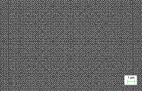
The fabricated octagonal structure analyzed in this work was determined by simulating the quasiperiodic transverse irradiance distribution given by eight-beam interference process and was theoretically analyzed through finite difference time domain simulations of the transmittance spectra.Citation6,Citation7 shows the SEM image of gold nanorods with an octagonal arrangement with diameter D = 125 nm and minimum interparticle distance Δ = 30 nm over an area of 150 × 150 μm.
Figure 1. Scanning electron microscopy (SEM) image of 2D octagonal quasiperiodic array of 125-diameter and 60 nm high cylindrical Au nanoparticles on quartz substrate (nearest center to center separation Δ = 30 nm and filling factor FF = 0.18)
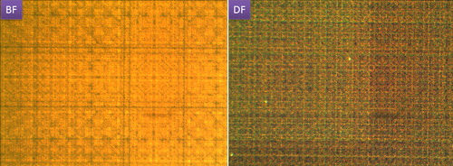
Dark field microscopy was used as a preliminary optical characterization of the plasmonic nanostructures. The color obtained from the dark field microscope is correlated to the scattering of the light by the nanostructures. Multiple light scattering from nanopatterned PQC structures, which occurs over a broad spectral angular range, leads to the formation of colorimetric fingerprints, in their near and far field zones, which can be captured with conventional dark field microscopy.Citation4 In , we reported array dark and bright field images of the fabricated octagonal structure.
Figure 2. Array dark and bright field images: octagonal structure was observed under × 100 objective with NA 0.8 and working distance 4.1 mm, and under × 20 objective with NA 0.4 and working distance 10.1 mm in reflection measurements
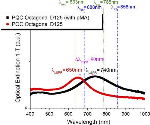
Optical transmission measurements were performed to locate the plasmon band for the samples prepared by EBL. UV-Vis absorption spectroscopy is routinely used for the characterization of plasmonic structures. The absorption spectra help us determine the spectral position of the plasmon resonance. shows the experimental extinction spectra of the PQC nanopattern before (red curve) and after (black curve) the probe (pMA) chemisorption. One dominant absorption maximum (two plasmonic modes) was obtained at λLSPR = 650 nm. The maximum of LSP resonance is observed to shift from 650 to 740 nm in case of the plasmonic structure with pMA probe chemisorbed. It should be noted that in experiments with excitation wavelength of 785 nm the Stokes Raman scattering wavelength corresponding to the band 1078 cm− 1 is 858 nm, which means that the maximum SERS effect can be achieved if the LSPR wavelength approaches near the mean value 821 nm.Citation17,Citation18,Citation22 Likewise, if an excitation wavelength of 633 nm is used, the band 1078 cm− 1 corresponds to 680 nm and the maximum SERS effect can be achieved for LSPR wavelength near to 656 nm. In this respect, the maximum value found for the LSPR wavelength of the octagonal (740 nm) is almost in the middle between 656 nm and 821 nm allowing the use of this structure for sensing applications in the visible near infrared regime. Two key characteristics are associated with the excitation of LSPRs: strong wavelength selective optical extinction in the far field and highly enhanced local electromagnetic fields in the near field. Optical properties such as extinction are determined entirely by the far field behavior of a plasmonic substrate (scattering, reflection, etc.), whereas SERS is a near field phenomenon that is generally maximized when the electric fields are as localized as possible. It has been demonstrated that there is an intricate relationship between the optical near field (as measured using SERS) and far field (as observed in transmission or reflection measurements).Citation18 Therefore, the optical signatures of LSPRs observed in transmission or reflection experiments are often used as a more convenient guide to the wavelengths at which a SERS substrate might be most effective.Citation23
Figure 3. Experimental extinction spectra of Au nanorods of diameters D = 125 nm (red curve) and pMA dosed Au PQC substrate (black curve) in air: shift in position of absorption bands is indicated with magenta line, and wavelengths of excitation λexc and Raman signal (λRS) are marked as vertical lines with green and blue respectively; spectra are acquired by transmission at normal incidence in air, with unpolarized light
Finally, the optical characterization of the fabricated nanostructure was performed using SERS. It has been well documented that SERS results from two effects, electromagnetic field enhancement caused by LSPR associated with metallic nanostructures and chemical enhancement caused by resonance Raman-like interaction between the metallic nanostructure and the adsorbate.Citation24,Citation25 It has also been demonstrated that large SERS signals are expected when both the frequency of the incident laser and the scattered Raman electromagnetic field approach the resonance frequency of LSPR.Citation17,Citation18,Citation22 The SERS signal from self-assembled pMA molecules has been measured and used to evaluate the SERS performance of the Au coated PQC plasmonic structure. Before the Raman experiments the SERS substrate have been immersed (overnight) in a 10 μM aqueous solution of pMA. In our experiments, the excitation wavelength is 785 nm.
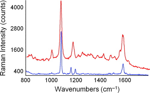
shows the SERS spectra of pMA adsorbed on the fabricated octagonal array and for comparison the spontaneous Raman spectrum of the molecule (bulk) is reported. This comparison highlights the strong enhancement of the Raman signal on the nanostructures and confirms the occurrence of the plasmonic effect for the probe molecule under investigation. The 1078 cm− 1 band intensity (one of the strongest Raman band for pMA) is used as an indicator for the enhancement on the nanostructured surface.
Figure 4. Raman spectra of bulk pMA (blue trace) compared with SERS spectrum of 10 μM pMA (red trace) adsorbed on Au octagonal nanocylindrical array, in range 800–1800 cm− 1: all Raman spectra were acquired with a diode laser of 785 nm and exposure time 10 s
The absolute enhancement factor was calculated as EF = RSENNREF/RSREFNEN, where RSEN and RSREF are the integrated area at a specific Raman band (at 1078 cm− 1, in our case) for the SERS and the spontaneous Raman spectrum respectively.Citation19,Citation20 Analogously, NEN and NREF represent, the number of molecules contributing to the measured signal on the nanostructure and in the bulk respectively. More specifically, the maximum number of molecules per nanoparticle and the total number of nanoparticles in the probe area determine the maximum surface number density (NEN) of adsorbate molecules that contribute to the measured SERS signal on the sample (namely, 6.7 × 10⁵ pMA molecules). Owing to the ability of pMA molecules to form a monolayer on metal surfaces,Citation12,Citation13 the number of molecules contributing to the SERS effect (NEN) can be estimated by the ratio of the total metal surface illuminated by the laser beam (radius of the spot) and the geometrical cross section of the individual pMA molecules (0.3 nm2 per molecule).Citation26 In order to calculate NEN, we evaluated the FF of our PQC pattern which reflects the ratio of the covered and the non-covered metal areas (FF = 0.18 in our case). On the other hand, NREF represents the average number of molecules in the scattering volume and is evaluated as NREF = BνDpMAA/MpMA, where Bυ is the optical excitation volume, DpMA is the density of pMA (1.06 g cm− 3) in the reference bulk crystal, A is the Avogadro number and MpMA is the pMA molecular weight (125.19 g mol− 1). The volume of the focal point Bυ was determined by measuring the change of the Raman signal of silicon (520 cm− 1) substrate as a function of the Z position of the objective.Citation19,Citation27 Experimentally, a silicon wafer immersed in solution is used to provide the confocal depth profile for the solution species. The Z profile measurements were obtained using a confocal Raman spectrometer (Horiba-Jobin Yvon Mod. Aramis) with the same operating conditions used for sample tests: diode laser excitation source emitting at 785 nm, metallurgical objective (MPlan × 100, NA = 0.9) with completely open confocal hole and slit apertures. By varying the focus of the laser on the silicon sample (Z profile), the intensity variation of the silicon peak shows a Gaussian-type variation. The full width at half maximum gives the waist length of the focal volume, the transverse dimension, i.e. the radius of the beam is determined in view of the NA of NA used for the specific wavelength (λLASER) according to the relation: 1.22λLASER/NA. An NREF of 5.6 × 10¹² pMA molecules in the laser spot was estimated. From here a maximum EF of 2.10 × 10⁷ was determined.
It should be noted, in respect to results obtained by Dal Negro groupCitation12 on structures with cylindrical pillars, that the higher value of EF measured in our work can be justified through: (1) optimized chosen geometric parameters; (2) the use of a morphology with a different simmetry and (3) from a greater number of pillars present in our structure.
Conclusions
In summary, we studied PQCs to develop innovative plasmonic nanobiosensors based on SERS and working in the visible/near infrared frequency band. Gold octagonal PQCs are proposed for the engineering of reproducible SERS substrates. Using a molecular monolayer of pMA as a probe molecule, we show that high values of SERS enhancement factors can be achieved in photonic structures: SERS enhancement factor of 2.10 × 10⁷ was achieved.
Conflicts of interest
The authors declare that there are no conflicts of interest.
Acknowledgments
This work was supported by the National Natural Science Foundation of China (Grant No. 601320106014) and by the European Regional Development Fund-FESR of POR Campania 2007-2013 - Call Innovation Window (Project title ‘‘Kit for Brucella Abortus e B. Melitensis nano-BIosensing RApid detection–AMBRA’’). We thank Mr Dong Chen from the Institute of Photonics of Ningbo University for the help in the Dark Field Measurements.
References
- Smith D. R., Padilla W. J., Vier D. C., Nemat-Nasser S. C. and Schultz S.: Phys. Rev. Lett., 2008, 4, 4184–4187.
- Vardeny Z. V., Nahat A. and Agrawal A.: Nat. Photonics, 2013, 7, 177–187.
- Cai W., Chettiar U. K., Kildishev A. V. and Shalaev V. M.: Nat. Photonics, 2007, 1, 224–227.
- Dal Negro L. and Boriskina S.: Laser Photonics Rev., 2012, 6, 178–218.
- Rippa M., Capasso R., Mormile P., de Nicola S., Zanella M., Manna L., Nenna G. and Petti L.: Nanoscale, 2013, 5, 331.
- Petti L., Rippa M., Zhou J., Manna L., Zanella M. and Mormile P.: Nanoscale Res. Lett., 2011, 6, 371.
- Zito G., Rose T. P., Di Gennaro E., Andreone A., Santamato E. and Abbate G.: Microwave Opt Technol. Lett., 2009, 51, 2732–2737.
- Maciá E.: Rep. Prog. Phys., 2012, 75, 036502.
- Levine D. and Steinhardt P. J.: Phys. Rev. Lett., 1984, 53, 2477–2480.
- Zheng W., Chiamori H. C., Logan Liu G., Lin L. and Chen F. F.: Nanotechnol. Rev., 2012, 1, 213–233.
- Anker J. N., Hall W. P., Lyandres O., Shah N. C., Zhao J. and van Duyne R. P.: Nat. Mater., 2008, 7, 442–453.
- Gopinath A., Boriskina S. V., Reinhard B. M. and Dal Negro L.: Opt. Express, 2009, 17, 3741–3753.
- Jackson J. B. and Halas N. J.: Proc. Natl Acad. Sci. USA, 2004, 1001, 17930–17935.
- Felidj N., Aubard J., Levi G., Krenn J. R., Salerno G., Schider G., Lamprecht B., Leitner A. and Aussengg F. R.: Phys. Rev. B, 2002, 65B, 075419.
- Haynes C. L. and van Duyne R. P. J.: Phys. Chem. B, 2003, 107B, 7426–7433.
- Stewart M. E., Anderton C. R., Thompson L. B., Maria J., Gray S. K., Rogers J. A. and Nuzzo R. G.: Chem. Rev., 2008, 108, 494–521.
- Grand J., de la Chapelle M. L., Bijeon L.-J., Adam P.-M., Vial A. and Royer P.: Phys. Rev. B, 2005, 72B, 033407.
- Doherty M. D., Murphy A., Pollard R. J. and Dawson P.: PRX, 2013, 3, 011001.
- Marquestaut N., Martin A., Talaga D., Servant L., Ravaine S., Reculusa S., Bassani D. M., Gillies E. and Lagugné-Labarthet F.: Langmuir, 2008, 24, 11313–11321.
- Gopinath A., Boriskina S. V., Premasiri W. R., Ziegler L., Reinhard B. R. M. and Dal Negro L.: Nano Lett., 2009, 9, 3922.
- Chirumamilla M., Toma A., Gopalakrishnan A., Das G., Proietti Zaccaria R., Krahne R., Rondanina E., Leoncini M., Liberale C., de Angelis F. and Di Fabrizio E.: Adv. Mater., 2014, 26, 15, 2352.
- Forestiere C., Miano G., Rubinacci G. and Dal Negro L.: Phys. Rev. B, 2009, 79B, 085404.
- Kahraman M., Daggumati P., Kurtulus O., Seker E. and Wachsmann-Hogiu S.: Sci. Rep., 2013, 3, 3396.
- Le Ru E., Etchegoin P., Chap. 3 and 4, ‘In principles of surface-enhanced Raman spectroscopy and related plasmonic effects’; 2009, Oxford, Elsevier.
- Campion A., Ivanecky J., Child C. and Foster M.: J. Am. Chem. Soc., 1995, 117, 11807–11808.
- Mohri N., Matsushita S., Inoue M. and Yoshikawa K.: Langmuir, 1998, 14, (9), 2343–2347.
- Ren B., Yao J. L., She C. X., Huang Q. J. and Tian Z. Q.: Internet J. Vibr. Spectrosc., 2004, 2, 2.