
Abstract
Background
A novel temperature dependent amorphous nano oxide semiconductor (AOS) thin-film transistor (TFT) is reported here for the first time, which is vastly different from conventional behavior. In the literature, the threshold voltage of TFTs decreases with increasing temperature. Here, the threshold voltage increased at higher temperatures, which is different from previously reported results and was repeated on different samples.
Methods
Electrical experiments (such as I-V measurements and photoelectron spectrometer experiments) were performed in order to explain such behavior. Double sweeping gate voltage measurements were performed to investigate the mechanism for the temperature dependent behavior.
Results
It was found that there was a change of trap charge under thermal stress, which was released after the stress.
Conclusion
Non-Arrhenius behaviors (including a linear behavior) were obtained for the amorphous nano oxide thin-film transistors within 303~425 K, suggesting their potential to be adjusted by measurement processes and be applied as temperature sensors for numerous medical applications.
Introduction
Amorphous oxide semiconductor (AOS) devices have been applied to a wide number of applications including as medical display circuits especially since 2004, when a typical amorphous oxide semiconductor, In-Ga-Zn-O (IGZO), was first published.Citation1–Citation4 They have a combination of advantages including transparency, flexibility, relatively higher mobility than amorphous Si-H (a-Si: H) and low temperature processing for large scale fabrication.
However, their temperature dependencies have been relatively less studied, which demands further investigation for potential applications. The display circuit working temperature range is up to 370 K.Citation5 Therefore, the temperature stability of AOS TFTs could impact their applications as medical display circuits. In most reports, their temperature dependencies are similar, i.e., the transfer curve shifts negatively with increasing temperatures.Citation5,Citation6
Besides, flexible and/or stretchable temperature sensors for humans are mainly in the range of 300–400 KCitation7–Citation9 for wearable human-activity monitoring and for personal health care. Temperature sensors for the human body mainly use either the thermo-resistive effect, pyroelectric effect, or thermoelectric effect. However, the presently reported flexible temperature sensors are based on nanomaterials fabricated either in solution-based processing methods or in direct printing/writing processes.Citation9 These methods have been reported to have less stability and repeatability than the processing of magnetron ratio frequency sputtering; besides, prominent methods include thermistor configurations. The resistance of thermistors varies in a nonlinear relationship with temperature, T, so that it is not very direct and convenient to have a good sensor with a linear relationship with T.Citation7
Here, the electrical properties change in a different manner than most conventional reports, and both the temperature dependence behavior of electrical properties and trap generation mechanisms are investigated and discussed. The transfer curves shift positively at higher temperatures, which is the opposite trend to most of the literature and was repeated on different samples. The degradation is commonly attributed to three components: i. Electron/hole trapping at the interface between the material layers; ii. Creation of ionized oxygen vacancies; and iii. Donor like defect creation in the IGZO channel.Citation3 In this paper, the gate voltage, VGS, sweeping to measure the transfer curves was clockwise, parallel shifting, and recoverable, so that the threshold voltage shift and hysteresis corresponded to the electron trapping/draping and/or the acceptor-like interface mechanisms.
Materials And Methods
The schematic of the sample with a bottom gate structure and a top channel with electrodes is shown in . The key material used as the TFTs channels for all experiments is a representative material of AOS, i.e., IGZO. The Si substrate was used as both the substrate and the bottom gate in the transistors. Another substrate was the PET plastic flexible plates. The dielectric layer was added on the bottom gate. Afterwards, IGZO was deposited by radio-frequency (RF) magnetron sputtering and the masks were employed to define the IGZO channel dimensions. Characterization experiments were performed using Keithley 4200, UPS (ultraviolet photoelectron spectroscopy) and SEM (scanning electron microscopy). The electrical experiments were performed with the TFT samples on the probe station.
Figure 1 (A) Schematic of nano amorphous oxide semiconductor (AOS) thin film transistors (TFTs). (B) SEM of the cross section of In-Ga-ZnO(IGZO) TFTs fabricated in lab (scale bar =100 nm).
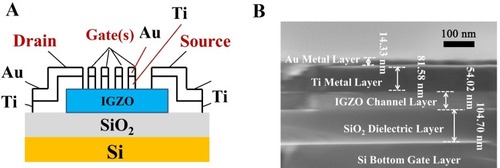
The detailed fabrication can be found in previous publications.Citation4 First, the IGZO channel was deposited on the SiO2 and Si substrates using the RF magnetron sputtering method. The power was 100 W. The gas ratio was Ar:O2=14:3. Secondly, the IGZO channel was patterned. Thirdly, the metal oxide electrodes were grown. Post annealing was performed to passive TFTs under 573 K for 1 hr. Electrical properties of the IGZO samples were measured from the drain terminal as the drain current IDS was investigated as a function of the voltage applied on the bottom gate terminal as shown in . A Keithley 4200 instrument was applied to measure the electrical properties, i.e., the channel current IDS versus the applied voltage on the terminals of the semiconductor devices. When a sweeping voltage was applied on the gate terminal with the source terminal voltage fixed at 0 V, the drain voltage was set at a certain value, 2~5 V, and the temperature T increased from 303 K to 453 K as the measured current, IDS, from the drain shifted gradually to the right-hand side.
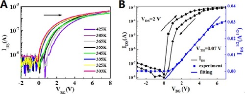
Figure 2 (A) Typical transfer curve degradation of the AOS TFTs samples under temperature stress. (B) Typical transfer curve loop of the AOS TFTs used here.
Results And Discussion
Temperature Stress Measurements
While some of our samples shifted to the left like previous publications, some others shifted to the right or shifted to both sides. This suggests at least two mechanisms corresponding to the curve shifts, with an additional mechanism to previous published dominant mechanisms. shows a typical transfer curve of the samples here under temperature stress. As shown in , the transfer curves of several samples, shifted to the right side when the temperature of the stress increased from 303 K to 453 K. The higher the temperature stress, the more to the right the transfer curve shifted. This right shift trend was opposite to previous reports of a left shift.Citation10–Citation12 This updated positive shift could be observed in over 3 samples from 303–425 K. It is hence suggested that more than one mechanism was responsible for the degradation. Among the mechanisms, one is for the left shift, and the other is for the updated right shift, which was dominant on more than one sample tested here and needs to be further investigated. The mechanisms for transistor degradation mainly contained three components: electron/hole trapping in the interface of different layers; oxygen vacancies; and donor-like interface trap generation. Because oxygen vacancies and donor-like traps are mainly responsible for the negative shift of the threshold voltage, the positive shift could be attributed to electron trapping.Citation3 Furthermore, the behavior in the reverse degradation trend of the device was due to donor-like traps and may even be attributed to acceptor-like traps.
Mechanism Under Temperature Stress
As shown in , the transfer curve showed a loop at the VGS sweeping, which suggested charge trapping. The loop was different from the direction of the anti-clockwise hysteresis, which claimed that the increase of the drain current was attributed to the partial desorption of the oxygen from the semiconductor during characterization.Citation3,Citation11 The clockwise loop suggested an electron trapping mechanism in the literature, which is additional evidence for the charge trapping mechanism during temperature stress.Citation3,Citation13
In order to clarify the mechanism behind the degradation under temperature stress, additional spectroscopy measurements were performed. As shown in , the UPS experimental results before and after temperature stress are shown. UPS reflects the electron structure information, where counts per second (CPS) are proportional to the number of trapped electrons. A higher UPS value corresponds to a larger amount of trapped electrons. The difference between before and after the temperature stress suggested differences caused by temperature stress. As shown in , the sample under temperature stress had a higher CPS, which suggested enhanced electron trapping. This may be attributed to the reason that because more electrons are scattered or trapped by the increased density in sample 2, and the current transport is depressed, there are less free electrons for channel currents. In this case, the current IDS at a higher temperature decreases at the same VGS and hence the IDS-VGS shifts to the right at a higher temperature.
Figure 3 (A) Ultraviolet ray photoelectron spectrometer (UPS) diagram of our AOSTFTs samples before temperature stress (sample 1) and after temperature stress (sample 2). (B) Linear fitting of threshold voltage Vth as a function of temperature T.
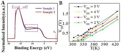
In order to model the relationship of temperature and the electrical property dependence of AOS TFTs, the threshold voltage, Vth, was plotted as a function of increasing stress temperature as shown in . shows the linear dependence of Vth on temperature T. A linear trend was found for the degradation of AOS TFTs in both subthreshold and saturation working status of the TFTs, which also showed a similar slope and intercept. This linear relationship suggested a potential to be a good sensorCitation10 for IGZO TFTs. This nice linear fit in and the fast recovery in suggested that the AOS TFTs have good potential as a candidate for medical temperature sensor applications.
Figure 4 Transfer curves IDS vs. VGS before (in blue), under (black) and after high temperature stress (red).
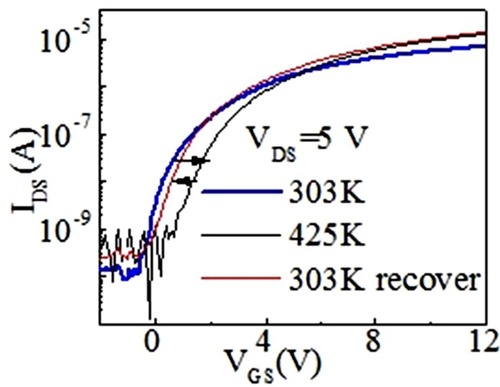
An optimal sensor should have a good recovery capability to a normal status. As shown in , the blue line represents the transfer curve, i.e. IDS-VGS, at a room temperature of 303 K. The black line stands for the transfer curve of IGZO TFTs at a higher temperature stress, i.e., 425 K. The red line is the transfer curve after the high temperature stress and under the 303 K temperature. As shown in , the temperature stress results in a transfer curve shifted to the right. The release of high temperature stress leads to a left shift of the transfer curve. The black line shifts to the right-hand side of the original blue line. The transfer curve shifts to the right when the temperature increases. The line in red is the transfer curve of IGZO TFTs under the temperature of 303 K after being heated to 425 K. The red line shifts back to the left side. This degradation and fast recovery is additional evidence of the existence of trap states at the semiconductor/dielectric interface. The percentage of the released charge under temperature stress was roughly 70% after 1 h of room temperature recovery, which suggested that the dominant degradation mechanism was charge trapping at the interface.Citation14–Citation17 Such recovery after the release of the temperature was found in all our sample measurements. This shows the potential of medical temperature sensor applications for our IGZO TFTs. The recoverable behavior can be adjusted more by adding proper passivation procedures.
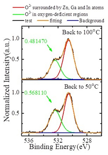
The recovery ability of our samples could be verified and explained by the in situ temperature XPS as shown in . This is because oxygen interstitials are considered to play a key role as donors and lead to free electrons for carrier conduction.Citation17 The oxygen vacancies correspond to mobile electron carriers and a 531.3 eV increase from above 0.7 when the temperature decreases. Now, the number of oxygen interstitials decrease after high temperature stress. In this way, a higher gate threshold voltage is required for the same number of electron carriers to turn on the channel, so that the transfer curves shift to the right side. This explanation is consistent with the observed experimental results. When the temperature decreases back, as shown in , the oxygen vacancies and thus number of electrons increase back again so that the threshold voltage decreases and the transfer curve shifts back to the left.
Figure 5 Temperature dependence of XPS for IGZO sample when the temperature decreases back.
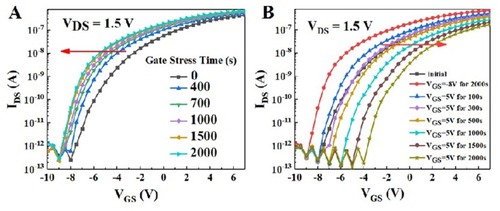
As shown in , when the negative gate pressure is applied continuously over a period of time, the transmission curve moves negatively and the longer the pressure is applied, the larger the negative shift; this is because of the bulk donor created by the gate stress.Citation18,Citation19 On the contrary, showed that when positive pressure was applied, the transmission curve moved positively. This is because the positive gate stress forced the captured positive charge to be released.Citation20,Citation21
Figure 6 (A) The transfer curve with VD=1.5V under different negative gate bias stress times. (B) The transfer curve with VD=1.5V under different positive gate bias stress times.
Conclusion
In this manuscript, we prepared temperature-sensitive AOS TFTs within the range of 303 K - 425 K. Considering all the present main working mechanisms (such as electron/hole trapping, oxygen vacancies and donor/acceptor like defects), we analyzed the temperature dependence of the AOS TFTs and proved that the threshold voltage shifted positively with higher temperatures. The degradation is mainly due to electron trapping at the semiconductor/dielectric interface which was verified by UPS and XPS. This AOS TFTs threshold voltage shift was linear to temperature and recovered fast, which suggests an AOS application as the temperature sensor for a wide range of medical applications.
Author Contributions
All authors contributed to data analysis, drafting and revising the article, gave final approval of the version to be published, and agree to be accountable for all aspects of the work.
Disclosure
The authors declare no competing financial interests.
Acknowledgments
The authors appreciate the help of Professor Mutsumi Kimura in the Department of Electronics and Informatics, Ryukoku University. This work was supported by the National Natural Science Foundation of China (Grant Nos. 61106090, 61574147, 61874078), Zhejiang Province Science Fund for Distinguished Young Scholars (Grant No. LR17F040002), Ningbo Municipal Natural Science Foundation (No. 2014A610011), the Ningbo Natural Science Foundation of China (Grant Nos. 2015A610034, 2011A610110, 2014B82004), the State Key Basic Research Program of China (2013CB922300), Youth Innovation Promotion Association, Chinese Academy of Sciences and the Royal Academy of Engineering, UK. The authors also appreciate the K.C. Wong Magna Fund in Ningbo University, China for funding.
References
- Fortunato E,Barquinha P, Martins R. Oxide semiconductor thin-film transistors: a review of recent advances. Adv Mater. 2012;24:2945. doi:10.1002/adma.20110322822573414
- Nomura K, Ohta H, Takagi A, Kamiya T, Hirano M, Hosono H. Room-temperature fabrication of transparent flexible thin-film transistors using amorphous oxide semiconductors. Nature. 2004;432:488. doi:10.1038/nature0309015565150
- Chen Y-J, Tai Y-H. Hysteresis of transistor characteristics of amorphous IGZO TFTs studied by controlling measurement speed. Ecs Solid State Lett. 2015;4:Q10. doi:10.1149/2.0041504ssl
- Dai M, Dai N. Logic circuit function realization by one transistor. Nano Lett. 2012;12:5954. doi:10.1021/nl303386b23075033
- Estrada M, Rivas M, Garduño I, et al. Temperature dependence of the electrical characteristics up to 370 K of amorphous In-Ga-ZnO thin film transistors. Microelectron Reliab. 2016;56:29. doi:10.1016/j.microrel.2015.10.015
- Zhang X, Zhai J, Yu X, Ding L, Zhang W. Fabrication and characterization of flexible Ag/ZnO schottky diodes on polyimide substrates. Thin Solid Films. 2013;548:623. doi:10.1016/j.tsf.2013.09.090
- Khan Y, Ostfeld AE, Lochner CM, Pierre A, Arias AC. Monitoring of vital signs with flexible and wearable medical devices. Adv Mater. 2016;28:4373. doi:10.1002/adma.20150436626867696
- Trung TQ, Lee N-E. Flexible and stretchable physical sensor integrated platforms for wearable human-activity monitoringand personal healthcare. Adv Mater. 2016;28:4338. doi:10.1002/adma.v28.2226840387
- Yao S, Swetha P, Zhu Y. Nanomaterial-enabled wearable sensors for healthcare. Adv Healthc Mater. 2018;7:1700889. doi:10.1002/adhm.v7.1
- Kim J, Bang S, Lee S, et al. A study on H 2 plasma treatment effect on a-IGZO thin film transistor. J Mater Res. 2012;27:2318. doi:10.1557/jmr.2012.199
- Estrada M, Gutierrez-Heredia G, Cerdeira A, et al. Temperature dependence of the electrical characteristics of low-temperature processed zinc oxide thin film transistors. Thin Solid Films. 2014;573:18. doi:10.1016/j.tsf.2014.10.092
- Vidor FF, Wirth GI, Hilleringmann U. Low temperature fabrication of a ZnO nanoparticle thin-film transistor suitable for flexible electronics. Microelectron Reliab. 2014;54:2760. doi:10.1016/j.microrel.2014.07.147
- Luo DX, Xu H, Li M, et al. Effects of etching residue on positive shift of threshold voltage in amorphous indium–zinc-oxide thin-film transistors based on back-channel-etch structure. IEEE Trans Elec. 2014;61:92. doi:10.1109/TED.2013.2292552
- Wilson DJ, Sudhir V, Piro N, Schilling R, Ghadimi A, Kippenberg TJ. Measurement-based control of a mechanical oscillator at its thermal decoherence rate. Nature. 2015;524:325. doi:10.1038/nature1449726258303
- Chen T-C, Chang T-C, Tsai C-T, et al. Behaviors of InGaZnO thin film transistor under illuminated positive gate-bias stress. Appl Phys Lett. 2010;97:112104. doi:10.1063/1.3481676
- Chowdhury MDH, Migliorato P, Jang J. Time-temperature dependence of positive gate bias stress and recovery in amorphous indium-gallium-zinc-oxide thin-film-transistors. Appl Phys Lett. 2011;98:153511. doi:10.1063/1.3580611
- Nayak PK, Hedhili MN, Cha D, et al. High performance solution-deposited amorphous indium gallium zinc oxide thin film transistors by oxygen plasma treatment. Appl Phys Lett. 2012;100:202106. doi:10.1063/1.4718022
- Ji KH, Kim J-I, Jung HY, et al. Effect of high-pressure oxygen annealing on negative bias illumination stress-induced instability of InGaZnO thin film transistors. Appl Phys Lett. 2011;98:103509. doi:10.1063/1.3564882
- Migliorato P, Delwar Hossain Chowdhury M, Gwang Um J, Seok M, Jang J. Light/negative bias stress instabilities in indium gallium zinc oxide thin film transistors explained by creation of a double donor. Appl Phys Lett. 2012;101:123502. doi:10.1063/1.4752238
- Um JG, Mativenga M, Jang J. Mechanism of positive bias stress-assisted recovery in amorphous-indium-gallium-zinc-oxide thin-film transistors from negative bias under illumination stress. Appl Phys Lett. 2013;103:033501. doi:10.1063/1.4813747
- Suresh A, Muth JF. Bias stress stability of indium gallium zinc oxide channel based transparent thin film transistors. Appl Phys Lett. 2008;92:033502. doi:10.1063/1.2824758