 ?Mathematical formulae have been encoded as MathML and are displayed in this HTML version using MathJax in order to improve their display. Uncheck the box to turn MathJax off. This feature requires Javascript. Click on a formula to zoom.
Abstract
The engineering of surface patterns is a powerful tool for analyzing cellular communication factors involved in the processes of adhesion, migration, and expansion, which can have a notable impact on therapeutic applications including tissue engineering. In this regard, the main objective of this research was to fabricate patterned and textured surfaces at micron- and nanoscale levels, respectively, with very different chemical and topographic characteristics to control cell–substrate interactions. For this task, one-dimensional (1-D) and two-dimensional (2-D) patterns combining silicon and nanostructured porous silicon were engineered by ion beam irradiation and subsequent electrochemical etch. The experimental results show that under the influence of chemical and morphological stimuli, human mesenchymal stem cells polarize and move directionally toward or away from the particular stimulus. Furthermore, a computational model was developed aiming at understanding cell behavior by reproducing the surface distribution and migration of human mesenchymal stem cells observed experimentally.
Introduction
Human mesenchymal stem cells (hMSCs) are increasingly used in therapeutic applications for bone, cartilage, and fat transplantation and repair.Citation1 MSC fates have been demonstrated to be controlled by oxygen, growth factors, substrate stiffness, geometry, micro-/nanostructure, and surface chemistry.Citation2–Citation4 Thus, in any biomaterial applications for bone tissue therapies, precise control of MSC adhesion and migration is a key factor. In this regard, surface micropatterns have been demonstrated to be a useful tool for the control of cell behavior.Citation5,Citation6 Additionally, surface nanotopography has been shown to exert influence over cell adhesion, morphology, proliferation, migration, differentiation, alignment, cytoskeleton organization, and gene expression in many cell types, including hMSCs.Citation7,Citation8 Cell migration on surfaces is a complicated process based on myriad cell–surface interactions, and plays a critical role in a variety of physiological and pathological phenomena.Citation9,Citation10 Cells respond to synthetic topographic surfaces in a wide variety of ways, which depend upon many factors including cell type, feature size and geometry, and the physicochemical properties of the substrate material.Citation11–Citation13
Although both micronscale and nanoscale surface topography have been known to be important in understanding cell–material interactions,Citation14 typically only simple patterns (eg, parallel lines or aligned posts) have been used in studying cell morphology, migration, and behavior. This restriction has limited the understanding of the multidirectional aspects of cell–surface responses.Citation15 Within this context, the main objective of this work is to fabricate patterned and textured surfaces at microscale and nanoscale levels, respectively, to control cell–substrate interactions. As such, here we present a method for the fabrication of surface patterns of different dimensionality (1-D and 2-D), aimed at studying cell adhesion and migration. The influence of surface morphology and chemistry on the adhesion and migration properties of hMSCs is studied. Although the basic mechanisms of random cell movement are well characterized, no single model explains the complex regulation of directional migration.Citation5 As such, here we propose a model to explain the surface migration of hMSCs in response to surface morphology and chemical state. For this task, computer simulations were performed with the aim of reproducing the experimental cell adhesion and migration characteristics of hMSCs.
Methods and materials
Fabrication and characterization of surface micropatterns textured at nanoscale level
Surface patterns were engineered by defining areas of monocrystalline silicon (Si) and nanostructured porous silicon (nanoPS). This material can be succinctly described as a rather complex network of Si nanocrystals with a large specific surface area.Citation16,Citation17 Additionally, its biocompatibility strongly depends on its porosity and pore size.Citation18 The surface micropatterns were fabricated as follows. Aluminum back contacts (~3000 Å) were deposited on the back side of boron-doped (p-type) monocrystalline Si wafers of <100> crystallographic orientation by electron-beam evaporation, followed by thermal annealing at 400°C for 5 minutes resulting in low-resistance ohmic electric contacts. Afterwards, the top surface of the silicon wafers was irradiated with MeV Si+ ions through micromasks (Gilder, Lincolnshire, UK) of different geometries, resulting in lowered conductivity in the exposed areas of the Si wafers. The MeV Si+ ion beam was supplied by the 5 MV electrostatic accelerator of the Centre for Micro Analysis of Materials (CMAM, Universidad Autónoma de Madrid). Lowered electrical conductivity in irradiated areas might have its origin in damage to the Si crystal structure and/or B dopant deactivation.Citation19,Citation20 The 1-D and 2-D patterns with well-defined areas of different conductivities are used to selectively grow nanoPS regions on the surface of the Si wafers. Accordingly, after mask removal the silicon wafers were galvanostatically etched in HF:ethanol electrolytes under illumination following a standard nanoPS fabrication process.Citation16,Citation21 The resulting surface patterns reproduce the geometry of the masks on the substrate; ie, nanoPS is selectively grown in non-irradiated areas while monocrystalline Si remains in irradiated regions.
Scanning-electron microscopy morphological characterization of the Si/nanoPS surface micropatterns was performed using a Hitachi S-3000N (Tokyo, Japan) equipped with a conventional thermionic filament. The operation voltage was set at 20 KeV.
Cell culture and immunofluorescence
Two to four milliliters of human bone marrow samples from healthy donors were provided by the Hospital Universitario La Princesa (Madrid, Spain). Cells were collected by centrifugation on 70% Percoll gradient and seeded at 200,000/cm2 in Dulbecco’s modified eagle’s medium–low glucose (DMEM-LG, Gibco, Paisley, UK) supplemented with 10% Fetal Bovine Serum (FBS) (Sigma). The medium was replaced twice per week. To perform the cell culture, the surface micropatterns were exposed to ultraviolet light for 10 minutes, thoroughly washed with phosphate-buffered saline (PBS), placed on a 24-multiwell plate (Falcon, Franklin Lakes, NJ) and seeded with 15,000 cells. The cells were then incubated for 72 hours with Dulbecco’s modified eagle’s medium–low glucose adjusted to 10% fetal bovine serum at 37°C in 5% CO2. After being washed twice with PBS the cells were fixed in 3.7% formaldehyde in PBS for 30 minutes at room temperature (RT). Cells were permeated with 0.5% Triton X-100 in C Buffer (100 mM NaCl, 10 mM Pipes pH 6.8, 3 mM MgCl2, 3 mM EGTA and 0.3 M sucrose) for 30 minutes at RT. Samples were blocked with 1% bovine serum albumin in PBS for 1 hour at RT. Surfaces were incubated in dark conditions for 1 hour with Alexa 488 phalloidin (1/100) and Dapi (1/5000) (Molecular Probes, Eugene, OR). Cells were visualized by a fluorescence vertical microscope Olympus IX81 coupled to a CCD color camera.
Results and discussion
Following the process described in the previous section, one-and two-dimensional surface micropatterns were fabricated using the appropriate mask for each case.
One-dimensional surface patterns
shows a characteristic 1-D Si/nanoPS surface pattern. Previous studies of surface morphology have demonstrated that the surface of nanoPS shows larger root mean square (rms) roughness than Si.Citation22 For scanning areas of 2 × 2 μm2, the surface rms roughness of nanoPS areas was found to be 1.1 nm, much larger than that of the silicon areas (0.2 nm). Additionally, the different surface wettability of Si and nanoPS is of key importance since it will contribute to determining the cell adhesion and migration characteristics. In a previous workCitation23 the wettability of both surfaces was studied in biological buffer conditions; it was found that the water contact angle decreases drastically from a superhydrophobic behavior (water contact angle = 126°) in the case of Si, to a neat hydrophilic character (water contact angle = 10°) for nanoPS. Moreover, cytotoxicity assays in human mesenchymal stem cells confirmed that porous silicon-based micro-and nanoparticles do not induce apoptosis.Citation24 Accordingly, the definition of Si/nanoPS surface patterns at microscale level leads to simultaneous chemical and nanotopographic contrasts, which will be subsequently used for the control of cell adhesion and migration.
Figure 1 Perspective scanning-electron microscopy images from a cross-section performed in micropatterns showing (A) alternating Si and nanostructured porous silicon stripes, (B) and Si/nanostructured porous silicon square grids. (C) Characteristic fluorescence from nanostructured porous silicon areas from a top view of a 2-D square pattern.
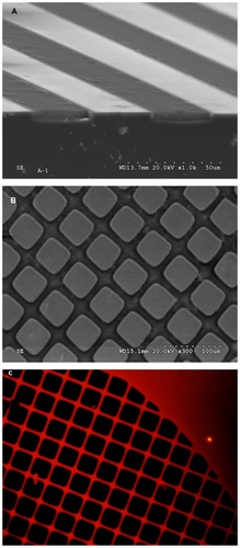
One-dimensional Si/nanoPS micropatterns consisting of alternating Si and nanoPS strips of different widths were fabricated, and the adhesion and migration of hMSCs studied after 72 hours of culture.Citation22 The experimental results indicated that in the case of 1-D surface patterns consisting of 100 μm-wide Si stripes and 25 μm-wide nanoPS stripes, hMSCs are preferentially found on Si areas as inferred from the location of the actin cytoskeleton and nuclei. For 1-D patterns consisting of alternating 50 μm-wide Si and 25 μm-wide nanoPS stripes, the cells appear predominantly on Si but occasionally also on the surface of nanoPS. By further reducing the width of the Si stripes to 35 μm while keeping the width of the nanoPS stripes (25 μm), the surface distribution of hMSCs was found to dramatically change. In this case, the actin skeleton is preferentially concentrated on Si areas while the nuclear environment, with notably reduced actin fiber intensity, is preferentially located on nanoPS areas.Citation22 The absence of hMSCs localized in nanoPS areas for large Si stripes and the inhibition of focal adhesion formation on nanoPS for any pattern suggest that the surface of nanoPS behaves as an antifouling platform given its surface roughness and particular chemistry as discussed above.
Two-dimensional surface patterns
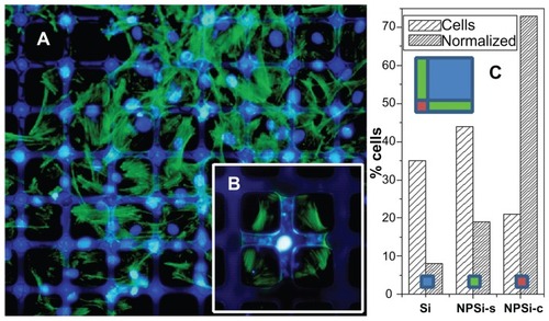
In order to confirm the previous results and to further advance our understanding of the migration behavior of hMSCs, 2-D patterns consisting of Si squares of 100 × 100 μm and 25 μm-wide nanoPS stripes were fabricated. shows a top view of a typical 2-D Si/nanoPS surface micropattern textured at nanoscale level. Fluorescence microscopy () shows a typical 2-D Si/nanoPS surface pattern, in which red photoemission indicates the location of nanoPS areas on the Si wafer. Fluorescence in the visible wavelength regime from nanoPS is a manifestation of quantum size effects given the nanometric size of the Si grains which compose nanoPS.Citation21 The experimental results show again that hMSCs respond to the particular structure of the 2-D patterns, as shown in . In this case, the distribution of the cytoskeleton is not evident but observation of the nuclei clearly indicates that cells are preferentially found at the intersection of the nanoPS stripes, as shown in . With the aim of extracting a behavioral trend, a bar diagram of nuclei categorized as belonging to the Si square areas, to nanoPS stripes, or to nanoPS “ intersections” has been represented (; see the schematic inset related to the different areas). It can be deduced from the area-normalized results that hMSCs migrate along the nanoPS stripes until they reach an intersection and nuclei are forced to assemble conformably. In cases when cells find themselves without neighboring competitors, they can adhere to and extend the cytoskeleton quasi-symmetrically at the intersection of two nanoPS stripes (). Finally, it is worth noting that the polarized structure of the actin cytoskeleton and the preservation of an internalized nucleus indicate that hMSCs cultured on the porous silicon-based micropatterns are far from an apoptotic stage.
Figure 2 (A) Fluorescence microscopy images of hMSCs on 100 μm Si/25 μm nanostructured porous silicon square micropatterns. Actin is stained green and nuclei are stained blue. (B) Detailed image at an intersection, and (C) histogram of hMSC population from image (A) with absolute % and area normalized population (left and right columns respectively).
Computer simulations
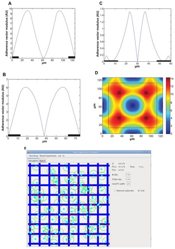
In order to get a deeper insight into cell surface distribution on 1-D and 2-D patterned substrates, cell surface migration was modeled and simulated. The basic idea behind our approach was to reproduce cell migration and final distribution on the patterned and textured substrates by the use of a simple mathematical model. In our model, cells are considered circular (with radius equal to 50 μm) and rigid, although they are allowed to partially overlap. With these assumptions, computer simulations follow two basic criteria, (1) cells tend to balance their adherence to the substrate and (2) cells tend to avoid overlapping with other cells.
According to criterion (1), cells tend to be attached to the Si substrate by distributing their adhesion surface equally around their center. This configuration is exemplified in where most cells show their actin fibers evenly distributed around the nuclei mainly on the surface of Si. In addition, the density of actin fibers increases with distance from the nuclei. Following these observations we have modeled how cell adherence is balanced around the nucleus by a vector – that we will name “center of adherence” – which is proportional to the center of “mass” of the cell, where only regions of the cell onto the Si areas are considered to have adherence or “mass.” In other words, the nanoPS areas are considered to have perfect antifouling properties and hence no cell parts on the nanoPS will exert any adherence force. In order to be balanced, cells tend to move to positions where the modulus of the center of adherence is zero. As such, cells perform a gradient descent on the center of adherence modulus. shows the adherence vector modulus for cells located on a line perpendicular to the 1-D stripe patterns for 100 μm-wide Si/25 μm-wide nanoPS alternating stripes (), 50 μm-wide Si/25 μm-wide nanoPS stripes (), 35 μm-wide Si/25 μm-wide nanoPS stripes (), and 2-D grid patterns consisting of 100 μm-wide Si and 25 μm-wide nanoPS stripes (). The coordinate origin has been placed in the center of the nanoPS stripes. The position of the nanoPS stripes has been marked with a black rectangle at the bottom of the plot (). In the case of 2-D patterns (), the black line indicates the location of the frontier between the Si surface and the nanoPS stripes. As such, the inner part corresponds to the Si surface whereas the outer part corresponds to the nanoPS stripes. Areas where a single cell is in equilibrium correspond to zero modulus areas. These areas correspond in the grid pattern to the center region of the Si area, the center region along the nanoPS side, stripes and to the intersections of nanoPS stripes. For the stripe patterns, the equilibrium regions for a single cell are along the center between two nanoPS stripes and on the nanoPS stripes.
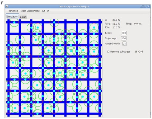
Figure 3 Adherence vector modulus for cells located on a line perpendicular to the 1-D stripe patterns for (A) 100 μm-wide Si/25 μm-wide nanostructured porous silicon (nanoPS) alternating stripes, (B) 50 μm-wide Si/25 μm-wide nanoPS stripes, (C) 35 μm-wide Si/25 μm-wide nanoPS stripes, and (D) one 2-D grid pattern of 100 μm-wide Si and 25 μm-wide nanoPS stripes. Screen capture of the program developed to perform the simulations and (E) t = 0, and (F) t = 400 seconds.
Regarding criterion (2) it is considered that cells deform themselves to adapt to their neighboring cells to avoid overlapping, as experimentally observed. This behavior has not been explicitly modeled, but in contrast cells, being considered circular, are allowed to partially overlap. However, cells tend to move in order to reduce the area that overlaps with other cells.
For the simulation, forces coming from criteria (1) and (2) have to be of the same order of magnitude. If too much weight is placed in (1) the simulation would finish with several cells at the same nanoPS intersections. On the other hand, if too much strength is given to (2) then all cells will finish packed independently of the substrate.
Migration of a cell located at position can be described as the gradient descent with respect to of the function
The first term of the summation corresponds to the modulus of the center of adherence and runs over all k parts of the cell that lie on the Si substrate, being the center of adherence and the adherence surface of part k. The second term of the summation corresponds to the interaction with other cells and runs over all cells being at a distance of less than 50 μm from the cell of interest. Here is the overlapping surface between cells at positions and , and K is a constant used to balance the relative strengths of both components.
Computer simulations were performed for the four surface patterns discussed above (ie, alternating Si/nanoPS stripes of different widths and 2-D square grid). All simulations are initialized with 150 cells randomly located in an area of 1000 × 1000 μm square. One hundred simulations are carried out for each pattern. shows screen captures of the program developed to perform the simulations at two different times (t = 0 seconds and t = 400 seconds). These two times correspond to the initial and equilibrium (final) states of the system, corresponding to the previous migration experiments, although the time scales are different. The position of the hMSCs on a single square grid is shown. shows the distribution of the cells for each pattern. Columns 2 and 3 indicate the initial and final percent distribution of hMSCs on the different substrates respectively. The final distributions are obtained after the system is in equilibrium.
Table 1 Surface distribution of the cells for the different Si/nanostructured porous silicon micropatterns
The simulation results are in good agreement with the experimental behavior observed experimentally. In the case of 1-D patterns, reduction of the width of the Si stripes results in increased cell surface coverage of the nanoPS areas. In the particular case of 1-D patterns with 35 μm-wide Si stripes, hMSCs are forced to locate preferentially on the surface of an antifouling surface (nanoPS) even though the percentage of Si surface is larger than that of nanoPS. In the case of 2-D patterns, the simulations reproduce the counterintuitive preference of hMSCs for the intersections of nanoPS stripes.
Conclusion
One- and two-dimensional micropatterns of silicon and nanostructured porous silicon were engineered by ion beam irradiation and subsequent electrochemical etch. These chemically and morphologically patterned surfaces have been exploited to control the surface distribution and shape of human skeletal progenitor cells and, at the same time, to study cell adhesion and migration characteristics. It was found that these cells are sensitive to surface patterns and that migration can be controlled, so that cells arrange in response to the particular surface topography and chemistry. As such the extra-cellular matrix impacts the mode and efficiency of cell migration. Finally, a mathematical model was developed and implemented, and allowed us to further understand surface cell distribution as a function of the dimensionality and size of the particular surface pattern. The proposed model is based on rather simple assumptions and parameterized through a center of adherence and the tendency of the cells to avoid overlapping. We have found that it constitutes a reasonable approach for the description of cell behavior on 1-D and 2-D surface micropatterns textured at nanoscale level.
Acknowledgments
The authors gratefully acknowledge financial support from MICINN under research project MAT2008-06858-C02-01/NAN, and grants from Fundación Domingo Martínez, and Comunidad de Madrid (Spain) under Project Microseres.
Disclosure
The authors have no conflicts of interest to declare in this work.
References
- LuoWJonesSRYousafMNGeometric control of stem cell differentiation rate on surfacesLangmuir20082421121291213318850687
- SarugaserRHanounLKeatingAStanfordWLDaviesJEHuman mesenchymal stem cells self-renew and differentiate according to a deterministic hierarchyPLoS One200948e649819652709
- D’IppolitoGDiabiraSHowardGARoosBASchillerPCLow oxygen tension inhibits osteogenic differentiation and enhances stemness of human MIAMI cellsBone200639351352216616713
- BallSGShuttleworthCAKieltyCMMesenchymal stem cells and neovascularization: role of platelet-derived growth factor receptorsJ Cell Mol Med20071151012103017979880
- PetrieRJDoyleADYamadaKMRandom versus directionally persistent cell migrationNat Rev Mol Cell Biol200910853854919603038
- DoyleADWangFWMatsumotoKYamadaKMOne-dimensional topography underlies three-dimensional fibrillar cell migrationJ Cell Biol2009184448149019221195
- YouMHKwakMKKimDHSynergistically enhanced osteogenic differentiation of human mesenchymal stem cells by culture on nanostructured surfaces with induction mediaBiomacromolecules20101171856186220568737
- BettingerCJLangerRBorensteinJTEngineering substrate topography at the micro- and nanoscale to control cell functionAngew Chem Int Ed Engl200948305406541519492373
- DiMillaPABarbeeKLauffenburgerDAMathematical model for the effects of adhesion and mechanics on cell migration speedBiophys J199160115371883934
- NgalimSHMagenauALe SauxGGoodingJJGausKHow do cells make decisions: engineering micro- and nanoenvironments for cell migrationJ Oncol2010201036310620652046
- YangCYHuangLYShenTLYehJACell adhesion, morphology and biochemistry on nano-topographic oxidized silicon surfacesEur Cell Mater20102041543021154247
- LawrenceBJMadihallySVCell colonization in degradable 3D porous matricesCell Adh Migr20082191619262124
- RanellaABarberoglouMBakogianniSFotakisCStratakisETuning cell adhesion by controlling the roughness and wettability of 3D micro/nano silicon structuresActa Biomater2010672711272020080216
- LiHKochharJSPanJChanSYKangLNano/microscale technologies for drug deliveryJ Mech Med Biol2011112337367
- JeonHHidaiHHwangDJHealyKEGrigoropoulosCPThe effect of micronscale anisotropic cross patterns on fibroblast migrationBiomaterials2010531154286429520189640
- LehmannVElectrochemistry of SiliconWeinheimWiley-VCH2002
- Martín-PalmaRJPascualLLandaAHerreroPMartínez-DuartJMHigh resolution transmission electron microscopic analysis of porous silicon/silicon interfaceApp Phys Lett20048525172519
- Martín-PalmaRJManso-SilvánMTorres-CostaVReview of biomedical applications of nanostructured porous siliconJ Nanophotonics20104042502-42501-20
- PoleselloPManfredottiCFizzottiFMicromachining of silicon with a proton microbeamNucl Instrum Meth B1999158173178
- BreeseMBChampeauxFJTTeoEJBettiolAABlackwoodDJHole transport through proton-irradiated p-type silicon wafers during electrochemical anodizationPhys Rev B200673id035428
- CanhamLTSilicon quantum wire array fabrication by electrochemical and chemical dissolution of wafersAppl Phys Lett19905710461048
- Munoz-NovalASánchez-VaqueroVPunzón-QuijornaEAging of porous silicon in physiological conditions; antifouling surfaces and scalable cell adhesionJ Biomed Mater Res ASubmitted
- GallachDRecio-SánchezGMunoz-NovalAFunctionality of porous silicon particles: Surface modification for biomedical applicationsMater Sci Eng B2010169123127
- Munoz-NovalASánchez-VaqueroVTorres-CostaVHybrid luminescent/magnetic nanostructured porous silicon particles for biomedical applicationsJ Biomed Opt20111602500221361682