 ?Mathematical formulae have been encoded as MathML and are displayed in this HTML version using MathJax in order to improve their display. Uncheck the box to turn MathJax off. This feature requires Javascript. Click on a formula to zoom.
Abstract
A silicon nanowire-based sensor for biological application showed highly desirable electrical responses to either pH changes or receptor-ligand interactions such as protein disease markers, viruses, and DNA hybridization. Furthermore, because the silicon nanowire can display results in real-time, it may possess superior characteristics for biosensing than those demonstrated in previously studied methods. However, despite its promising potential and advantages, certain process-related limitations of the device, due to its size and material characteristics, need to be addressed. In this article, we suggest possible solutions. We fabricated silicon nanowire using a top-down and low cost micromachining method, and evaluate the sensing of molecules after transfer and surface modifications. Our newly designed method can be used to attach highly ordered nanowires to various substrates, to form a nanowire array device, which needs to follow a series of repetitive steps in conventional fabrication technology based on a vapor-liquid-solid (VLS) method. For evaluation, we demonstrated that our newly fabricated silicon nanowire arrays could detect pH changes as well as streptavidin-biotin binding events. As well as the initial proof-of-principle studies, C-reactive protein binding was measured: electrical signals were changed in a linear fashion with the concentration (1 fM to 1 nM) in PBS containing 1.37 mM of salts. Finally, to address the effects of Debye length, silicon nanowires coupled with antigen proteins underwent electrical signal changes as the salt concentration changed.
Introduction
Real time monitoring of biological change due to the presence of disease is a crucial aspect of diagnosis, because early detection is fundamental to cure or prevention before such disease becomes untreatable. To this end, antigens have been widely used as target molecules for immunodetection techniques. Their high sensitivity has enabled the detection of abnormalities. However, most immunodetection techniques to date have used probes labeled with radioactive isotopes, enzymes, or fluorescent dyes and rely mostly on imaging or analysis tools for detection.
The silicon nanowire (siNW) field effect biosensor has received considerable attention as a revolutionary electrochemical sensing method since its development in recent years (CitationCui et al 2001) and has provided a new direction in the diagnosis of disease. The sensing mechanisms differ from assays, such as imaging with contrast agents (CitationArtemov et al 2003; CitationGao et al 2004; CitationLoo et al 2005), immunoassays (CitationWard et al 2001), and the surface plasmon resonance method (CitationCampagnolo et al 2004). For example, siNWs can be produced by a straightforward fabrication method (top-down or bottom-up approaches), have high sensitivity compared with conventional disease screening, and allow real time detection without the need of extra labels necessary for measurements (CitationCui et al 2001; CitationBunimovich et al 2006). Because of these characteristics, siNWs have been widely studied as biological detection methods including streptavidin-biotin binding (CitationCui et al 2001), disease protein detection based on antibody-antigen interaction (CitationZheng et al 2005), viruses (CitationPatolsky et al 2004), and DNA hybridization (CitationLi et al 2004).
However, previous bottom-up approaches have shown that high end device integration using nanowires is hard to achieve, because of high costs and difficult-to-control processes. Although recent studies (CitationBunimovich et al 2006; CitationStern et al 2007) demonstrated that top-down approaches might overcome intrinsic degradation caused by the reactiveion-etching (RIE) of the silicon layer, and showed high sensitivity on pH (CitationStern et al 2007) and DNA hybridization (CitationBunimovich et al 2006), the problem of transferring to suitable substrates for device integration remains unresolved. In addition, the presence of salt in phosphate buffered saline (PBS) or blood samples necessitates salt screening, in other words the Debye screening effect, which reduces the efficiency of signal detection (CitationHeitzinger and Klimeck 2007). Therefore, easy access to substrate and salt control are major obstacles that must be addressed in order to succeed in integrating siNWs arrays in high throughput-sensing devices.
To meet these needs, we propose a top-down method to fabricate siNWs, which is more like the conventional micromachining process than other siNWs fabrication approaches. This process is composed of reactive ion etching (RIE) followed by the KOH wet etching process. The latter was added to avoid the intrinsic degradation that is part of the RIE process. Our new method of transferring ensures that the siNW array is well aligned with the substrate, and has a high yield.
In addition, we can report preliminary investigations on the electrical responses to pH changes and antigen/antibody interactions, such as streptavidin-biotin and C-Reactive Protein (CRP) which is a well known indicator for stroke, cardiovascular disease (CVD), and inflammation. A quantitative analysis of salt concentration in PBS was made, which would be the first step to consider for further refinement, in order to improve the siNW sensitivity to particular disease proteins. To evaluate the signal changes in salt solution, we measured pattern changes of target molecules and their antibody reactions in different salt concentrations (137 mM, 13.7 mM, and 1.37 mM) in PBS. The electrical signal changes according to salt concentrations suggest that the amount of signal amplification can be measured as long as antibodyantigen interactions are occurring on the surface of siNWs. Finally, the passivation of electrodes shows high sensitivity compared with previously reported results (CitationLee, Kim et al 2007) (data are not shown here). Therefore, based on results demonstrated in this article, the design of our siNW array suggests the possibility of nanometer-scale biosensor integration.
Experimental method
Silicon nanowire fabrication
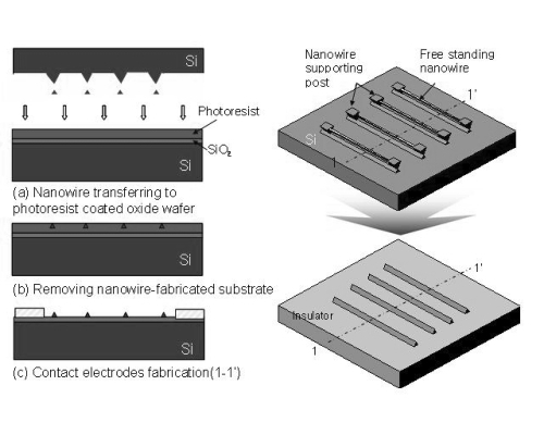
We followed the process described in previous work (CitationLee, Lee et al 2007). Silicon nanowire (SiNW) was simply fabricated by a conventional micro-machining technology based on photolithography, anisotropic etching, and thermal oxidation processes. In general, for the fabrication we used single crystalline silicon substrate, with p-type (100)-oriented substrate characterized by 0.01–0.02 Ωcm and 10–30 Ωcm and n-type (100)-oriented substrate. All substrates were 100 mm in diameter (4 inch wafer). The electrical properties of silicon nanowire can be controlled by choosing a silicon substrate with an intended dopant type and concentration. Starting with thermal oxidation of silicon substrate, 0.8 to 1 μm wide, lines of oxide layer are defined using stepper photolithography. Silicon bulk anisotropic etching, using deep silicon reactive-ion-etching (DRIE) and potassium hydroxide (KOH) solutions in sequence, provides an inverted triangular shape, in cross-section, of silicon lines supported by narrower silicon pillars as shown in process step (C) in . Because anisotropic wet etching of single crystalline silicon in KOH solutions gives this triangular type structure determined by (111) the etch stop plane of silicon, (110)-oriented silicon lines created a uniform and constant diameter. Thermal oxidation of the silicon substrate follows, producing a silicon nanowire with a sub-100 nm diameter near the center of an inverted triangle (), while the supporting silicon pillar becomes completely oxidized. The nanowire becomes free-standing, after the surrounding SiO2 is removed (). The manufacture of the nanowire array, and the procedures to transfer siNWs on to the insulating surface, are schematically described in . First, the free standing siNWs were transferred to the photoresist layers on an insulating wafer. Subsequently, the siNWs underwent removal of photoresist followed by electrode formation. Compared with other previous bottomup approaches, or silicon on insulator-based top-down approaches, our transferring process has the advantage of being relatively straightforward, and can be used to achieve easy attachment to any substrate.
Figure 1 Fabrication of silicon nanowires with top-down approach including (a) thermal oxidation, (b and c) stepper photolithography followed by bulk anisotropic etching by deep silicon reactive ion etching (DRIE), and (d) thermal oxidation with post-potassium hydroxide (KOH) solution. Their corresponding SEM images are shown in (b and d).
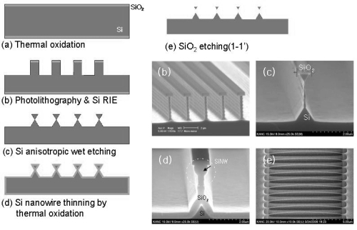
Figure 2 SiNWs transfer process for nanowire assembly (left) and their prior and post transfer (right). Free standing siNWs were transferred to photoresist layers on wafers.
Silicon nanowire surface modification
The procedure used to functionalize the siNW surface is clearly described elsewhere (CitationLobert et al 2003; CitationPatolsky et al 2006). The procedure resulted in an aldehyde-terminated monolayer on siNWs surfaces. Briefly, organic materials were cleaned off with oxygen plasma for 5 minutes. Cleaned and hydrophilic siNWs were treated with 2.5% (v/v) 3-aminopropyltriethoxysilane (Sigma Aldrich Ltd, St Louis, MO) in ethanol for 90 minutes followed by incubation in 1.25% glutaraldehyde (Nanobest Inc., Seoul, Korea) in PBS for 120 minutes. The glutaraldehyde is affected by condensation cross linking with the amine group. The terminal aldehyde group can react with anti-CRP (100 μg/ml in PBS, pH = 7.4). The anti-CRP attached siNWs were then assigned for conductance change by the antigen-antibody interaction. Antigen proteins were also purchased, and reconstructed in appropriate PBS medium for the experiments.
Electronic measurements
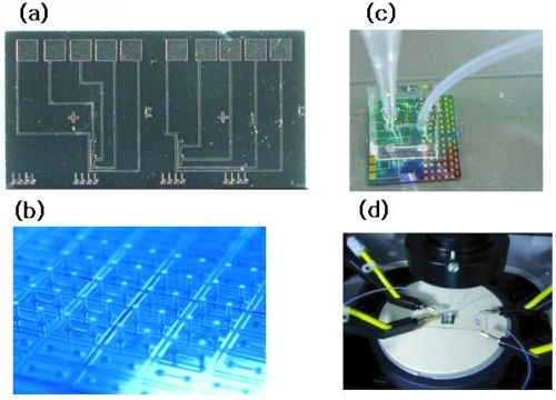
For the quantitative measurements of siNW responses to different salt concentrations, a PDMS well-type channel was designed and manufactured. This channel was positioned on the chip, allowing solution to be delivered, stationed on nanowire arrays, and aspirated with a syringe pump. Measurements were performed with a Keithley 2400 source meter (Keithley Instruments, Inc., Cleveland, OH); a twopointed probe (). A -500 mV (VDS) was applied to one terminal of the nanowire for the measurements. shows the top view of the siNW chip (a), the PDMS channel (b), the tube for solution delivery (c), and probe station tips (d). The average size of siNWs used in these experiments is approximately ~70 nm in diameter and 30 μm in length.
Figure 3 Electrical signal measurement system composed of (a) siNWs chip device, (b) PDMS with channel, inlet, and outlet, (c) chip with PDMS channel connected to syringe pump and outlet tube, and (d) chip-mountable probe station.
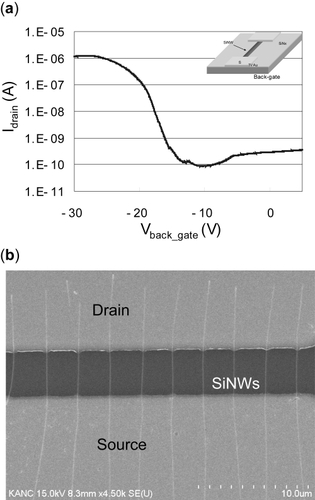
Before the biosensing experiment, SiNW FET characteristics were evaluated using back-gate configuration. A p-type nanowire FET with diameter of 100 nm was estimated. A 300 nm thick low pressure chemical vapor deposition (LPCVD) Si3N4 layer was used as dielectric material and p-doped Si (Rs = 10 Ωcm, specific resistance of substrate) was used as a global back-gate. Typical current vs. gate voltage (IDS vs. Vgs) characteristics of the back-gated NW FETs exhibit high Ion/Ioff (over 104), ON-state current of the order of ~ 1 μA (VDS = −1V) per 10 NWs ().
Figure 4 (a) FET characteristics of SiNW device using back-gate modulation; (b) SiNW FET device for biosensor application.
Electrode passivation
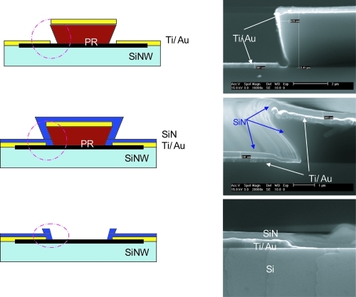
Since both the siNW arrays and the electrode must be immersed in the solution, the electrode region should be covered by the insulator in order to block the possible current loss or antibodies and increase sensibility. We used Si3N4 for passivation because of its weaker reaction to antibodies than silicon. The passivation process and corresponding figures are shown in .
Figure 5 Schematic drawing of the process flow for passivation (left) and corresponding SEM images (right).
Results and discussion
and show verification of the ability of siNWs to work as an ion-based FET. In , two different p-type siNWs were used to measure the under source of −0.4 V with the addition of buffers from pH 10 to pH 4 (a) and in reverse (b), respectively. As in previous work, protonation and deprotonation were mainly responsible for the rapid changes in conductance as a function of pH variations (CitationCui et al 2001). Briefly, the amine group (NH2) on the nanowire surface is protonated () in low pH conditions, which has a positive gate effect on nanowire arrays and therefore causes hole depletion and increases resistance. In higher pH conditions, the silanol group (SiOH) on the nanowire surface gets deprotonated and plays a major role, providing a negative gate effect on arrays. This deprotonation leads to hole accumulation and resistance decrease. Because signal changes are closely related to surface modification processes, the changes in sensitivity to pH further demonstrate the presence of the amine group on nanowire surfaces.
Figure 6 (a) Electrical signal change according to pH variation (pH 4 ~ 10) and (b) pH 10 to 4 at source voltage of −0.4 V with p-type siNWs. Average size of siNWs is diameter 70 nm and length 20 μm.
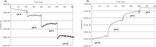
Figure 7 Graphs show experimental results from the (a) signal changes with increasing streptavidin concentration and (b) their average, and the variations of each concentration. They are mean of 4 values ± 2 SD.
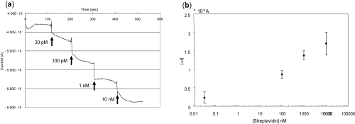
shows the real time electrical response of siNWs when exposed to streptavidin solutions (30 pM to 10 nM). The siNWs used here were p-type and their surfaces were functionalized with biotin receptors. The pH value of the PBS (pH = 7.4) solution was higher than the isoelectric point (pI) of the streptavidin. Because pI (Streptavidin) ≈ 5, current signals decreased with the addition of streptavidin at the potential of −0.4 V, a small but noticeable signal change was observed when 30 pM of streptavidin was injected. Further addition of a higher concentration of streptavidin (100 pM to 10 nM) began to weaken the signal instantly, and continued to weaken it as concentration increased. The mean signal from four measurements and their variations are presented in ; the individual point represents the averaged differences between streptavidin solution addition and baseline (prior to streptavidin addition). In these initial studies, our top-down-based siNWs, which showed high performance of FET characteristics, generally exhibit high sensitivity in charged particle (eg, protein) detection as well.
The real time electrical signal increases of the siNWs upon addition of CRP was observed (). The signal changes due to CRP binding were measured for CRP concentrations from 1 fM to 1 nm. Before the addition of CRP, low salt (1.37 mM) containing PBS was delivered over the siNWs. The results show that siNWs express noticeable signal changes even as low as in 1 fM (), suggesting that low salt ions can increase the Debye length which was approximately 1 nm in the blood or serum (CitationHeitzinger and Klimeck 2007). As demonstrated in and the literature (CitationHeitzinger and Klimeck 2007), the Debye screening length is increased by more than 8 nm when the physiological electrolyte solution is close to 1 mM. In this low salt condition, the gating effect is likely to be easily delivered on to the surface of the siNWs. In addition, compared to other molecules such as PSA and CEA, which have a larger molecular weight (160 kDa), CRP has relatively less (26 kDa). Smaller molecules help electrochemical sensing take place near the siNW surface which has an overall increase in sensitivity.
Figure 8 Real-time electrical signal measurements: (a) Signal changes with systematic delivery of 1 fM, 1 pM, and 1 nM of CRP antigen in low salt concentration (1.37 mM) and (b) signal changes from before delivery of CRP antigen. They are mean of 3 values ± 2 SD.
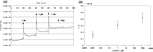
Figure 9 Real-time electrical signal measurements. Signal changes with systematic delivery of 1.37 mM, 13.7 mM, and 137 mM of PBS (left figure) and their signal changes from the base line, which corresponds to each signal at 137 mM. They are mean of 3 values ± 2 SD.
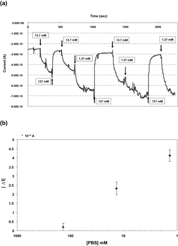
Lastly, we evaluated the efficacy of the salt concentration at mediating signal changes. The Debye screening length increased exponentially with salt concentration to as low as 1.37 mM. At this concentration, the Debye length was estimated at more than 8 nm (CitationHeitzinger and Klimeck 2007). This can be rapidly decreased by the addition of salt to the solution, which can mask the surface charge on nanowires. In our studies, greater concentration relevant to experimental investigation of the signal was achieved by measuring changes due to salt concentrations. While CRP antigens remain bound with antibodies, a different concentration of salt solution (1.37~137 mM) was added into the PDMS channel. Current signals were changed interactively and instantly as salt was delivered to the channel (). The signal variation was thus specific to and reversible with concentration. The dynamic range was measured as 4.2 * 10−10 amperes between the lowest peak (1.37 mM) and the highest (137 mM).
As electrolyte solution containing low salt concentration was injected, the Debye length increased enabling the previously undetectable signal to be sensed. This condition gives rise to signal features that are more obvious at the lowest concentrations (1.37 mM). The results here agree with the published study, indicating that salt concentration can determine sensitivity (CitationHeitzinger and Klimeck 2007).
Conclusion
Nanowire-based electrical sensing of biological interactions between disease antigens and their specific antibodies have demonstrated a higher sensing efficiency, without the need of extra chemical processes to tailor antibodies to labels. Furthermore, all the results could be displayed in real time, because the sensing mechanism does not need secondary measurement systems.
Prior studies have shown that the future direction of disease diagnosis, DNA examination, and virus detection could change dramatically. Nano-bio-electro technologies aim to improve sensitivity, monitoring, and detecting of biomolecules, which can obtain earlier and greater accuracy in disease detection. Our investigations have shown that silicon nanowires based on a top-down approach, which follows our newly designed method, obtained comparable results in detecting disease protein markers to previously published results. Note that based on the results shown to date, the sensing ability of siNWs is highly dependent on salt concentration in solution due to the fact that Debye length is a function of salt concentration. In order to improve this sensing ability, either sensing event should take place within the Debye length, or salt concentration should be reduced to increase the Debye length. Prior to these considerations, the range of signal changes should be addressed with the same experimental conditions other than salt concentrations. Our well-type PDMS channel could be suitable for quantitative measurement of the sensitivity of siNWs to salt concentration. This system helps to station the solution in the channel while the signal measurement is being made, and aspirate it out post measurement. Results indicate that 1.37 mM of salt containing PBS displays the highest signal change in this study. Therefore, we could retrospectively determine the concentration of salt from the current signal.
Other than biological sense, the micromachining process used in fabricating siNWs was very stable and could produce a large amount of well ordered siNW arrays on any substrates with ease, preserving comparable properties for the biosensor purposes.
Our modified top-down approach may provide promising new ways to create useful tools for commercializing siNWs-based devices for diagnosis in clinics as well as high tech physical sensors.
Acknowledgements
This work has been supported by Grant No. 10023796 from the Regional Technology Innovation Program of the Ministry of Commerce, Industry and Energy. There is no conflict of interest.
Reference
- ArtemovDMoriNOkollieBMR molecular imaging of the Her-2/neu receptor in breast cancer cells using targeted iron oxide nanoparticlesMagn Reson Med200349403812594741
- BunimovichYLShinYSYeoW-SQuantitative real-time measurements of DNA hybridization with alkylated nonoxidized silicon nanowires in electrolyte solutionJ Am Chem Soc2006128163233117165787
- CampagnoloCMeyersKJRyanTReal-time, label-free monitoring of tumor antigen and serum antibody interactionsJ Biochem Biophys Methods2004612839815571777
- CuiYWeiQParkHNanowire nanosensors for highly sensitive and selective detection of biological and chemical speciesScience200129312899211509722
- GaoXCuiYLevensonRMIn vivo cancer targeting and imaging with semiconductor quantum dotsNature Biotech20042296976
- HeitzingerCKlimeckGComputational aspects of the three-dimensional feature-scale simulation of silicon-nanowire field-effect sensors for DNA detectionJ Comput Electron2007638790
- LeeK-NKimW-HJungS-WCharacteristics of silicon nanowire field effect transistors fabricated by micromaching process2007The 9th Korean MEMS ConferenceJeju, l
- LeeM-HLeeK-NKimASilicon nanowire based anitbody specific and label free sequece specific biosensor2007KMEMS 2007Jeju, I
- LiZChenYLiXSequence-specific label-free DNA sensors based on silicon nanowiresNano Letters200442457
- LobertPEBourgeoisDPampinRImmobilization of DNA on CMOS compatible materialsSensors and Actuators B2003B 929097
- LooCHirschLRLeeM-HGold nanoshells bioconjugates for molecular imaging in living cellsOptics Letters20053010121415906987
- PatolskyFZhengGHaydenOElectrical detection of single virusesPNAS2004101140172215365183
- PatolskyFZhengGLieberCMFabrication of silicon nanowire devices for ultrasensitive, label-free, real-time detection of biological and chemical speciesNature Protocols20061171124
- SternEKlemicJFRoutenbergDALabel-free immunodetection with CMOS-compatible semiconducting nanowiresNature20074455192217268465
- WardAMCattoJWFHamdyFCProstate specific antigen: biology, biochemistry and available commericial assaysAnn Clin Biochem2001386335111732646
- ZhengGPatolskyFCuiYMultiplexed electrical detection of cancer markers with nanowire sensor arraysNature Biotech2005231294301