 ?Mathematical formulae have been encoded as MathML and are displayed in this HTML version using MathJax in order to improve their display. Uncheck the box to turn MathJax off. This feature requires Javascript. Click on a formula to zoom.
Abstract
A homemade microwave plasma-enhanced chemical vapor deposition method was used to grow a multiwalled carbon nanotube between two nickel catalyst electrodes. To investigate the transport properties and electron scattering mechanism of this interconnection (of approximately fixed length and fixed diameter), we carried out a model analysis of temperature dependence of resistivity. To explain the abnormal behavior of the negative temperature coefficient of resistivity in our experimental results, we then employed theories, such as hopping conductivity theory and variable range hopping conductivity theory, to describe resistivity in the high- and low-temperature ranges, respectively. Further, the grain boundary scattering model is also provided to fit the entire measured curve of temperature dependence of resistivity.
Introduction
Nanoscale electronic devices are expected to become more and more integral to future high-performance integrated circuit devices, due to their intrinsic properties regarding latency and power dissipation. To further advance silicon-integrated circuit (IC) technology, the high-speed transmission needs of chips must be taken into account, and the novel properties of carbon nanotubes (CNTs) show exciting promise for leading future IC chip interconnect developments.Citation1 The extremely low density of CNTs as solids, ie, 1.3–1.4 g/cm means their specific strength is up to 48,000 kN/m/kg, which is the best specific strength of all known materials, comparing well with the specific strength of high-carbon steel, ie, 154 kN/m/kg.Citation2 In theory, metallic nanotubes can carry an electrical current density of 4 × 10⁹ A/cm2, which is more than 1000 times greater than that able to be carried by copper. While their electronic transport properties have attracted significant interest,Citation3–Citation5 CNTs might also play a pivotal role in the fabrication of electronic nanoscale devices due to their unique mechanical flexibility,Citation6 resistance to chemical corrosion,Citation7 and high field emission properties.Citation8
These exciting properties are dependent on the structure and synthesis of the CNTs. Theoretically, in pure metallic single-walled carbon nanotubes (SWCNTs) or multiwalled carbon nanotubes (MWCNTs), electron transport would occur ballistically, such that electrons would transport along the nanotube axis without any power dissipation due to scattering.Citation9,Citation10 Thus, electrons and phonons would propagate easily along the same tube axis.
However, in practice, there are many structural factors involving the synthesis of CNTs to consider, eg, defects (impurity, vacancy) or grain boundary in/on the CNTs. Extensive research and literature are devoted to understanding and finding solutions for improving CNT structural defects and problems. Naeemi and Meindl used equivalent circuit models to simulate various electron-phonon scattering mechanisms as a function of temperature and to model the temperature coefficient of resistance (TCR) for different types, defects, and lengths of CNTs.Citation11 Resistivity is influenced by certain defects (such as Stone–Wales defects and the Aharonove–Bohm effect), as well as catalysts remaining in the CNTs that cause extra scattering and interface roughness.Citation12,Citation13 Structure defects of the material, such as interface roughness and small grain size, also cause variations of the electron transport characteristics.Citation8 Self-heating also plays a significant role in short-length nanotubes transporting current under high bias.Citation14 Svizhenko et al reported that “large diameter nanotubes are preferable because even the semi-conducting shells can carry current due to small band gaps”, and “the conductance decrease with increase in bias was caused by reflection of incident electrons at crossing subbands due to scattering with zone boundary phonons”.Citation15
In our work, using the concept of phenomenology, we attempt to fit a temperature dependence of resistivity model to the experimental high-to-low temperature range (300–25 K), with results from an individual MWCNT (of approximately fixed length and diameter) shown in . This particular MWCNT was fabricated using a homemade microwave plasma-enhanced chemical vapor deposition (MPECVD) system.Citation4,Citation16 In order to explain the result of a negative TCR, we took into account the theories of hopping conductivity, variable range hopping conductivity, strong localization (kf l 0 ~ 1, in the product kf l0, where kf is the quasi-Fermi wave vector, l0 is a finite mean free path, and reflects the degree of the disorder and localization) and grain boundary scattering.Citation17
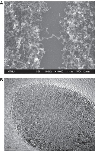
Figures 1 A) The scanning electron microscopic image of a multiwalled carbon nanotube which was grown at 650°C and 10−5 torr with a 3 µm length and 100 nm diameter between two isolated electrodes as a current conduction bridge.Citation4,Citation16 B) A cross-sectional image of another sample of the same batch of multiwalled carbon nanotubes.
Theory
Hopping conductivity
If the number of impurities or defects in the crystalline structure increases, then electron wave function spans only a few lattices and fades exponentiallyCitation18 Therefore, the conductivity is varied due to electron tunneling between localized states, and a negative TCR arises from phonon-assisted hopping conduction. Excitation of electrons to Ec which contributes to conductivity by hopping can be expressed as strongly localized states:
Where Ec is the mobility edge and EF is the Fermi energy. This form of conduction is normally predominant at relatively high temperatures, or when (Ec–EF) is small (for small value of Ec–EF, the transport path and the typical hopping distance are defined respectively).Citation19
Variable range hopping
Thermally activated variable range hopping conduction by electrons in the states near the Fermi energy at low temperaturesCitation18 is described as:
Where R is the hopping distance, vph denotes the phonon energy, B is the coefficient related to the density of state, and d indicates the dimension. This condition occurs at sufficiently low temperatures.
Grain boundary scattering
Mayadas and Shatzkes were the first researchers who explored the theory of boundary scattering of electrons in thin, polycrystalline, metal films.Citation20 However, Hoffmann et al empirically proposed a superior method to take into account and explain the boundary scattering of electrons.Citation21 The conductivity of thin, polycrystalline films strongly deviates from the conductivity of its corresponding bulk single crystalline materials. Hoffmann et al stated that the reduction of conductivity depends exponentially on the number of grain boundaries per mean free path (MFP), and all electrons reflected by the grain boundaries along one mean free path do not contribute to the resulting current. The DC conductivity of polycrystalline films can be assumed as:
Where l∞/RG is the number of grain boundaries per mean free path and Tg is the average probability for an electron to tunnel a single grain boundary, such that the effective mean free path can be expressed as:
where l∞−1 = lo−1 + lin−1 is due to Matthiessen’s lawCitation22 Here, lo is the elastic mean free path resulting from acoustic phonon scattering, while the temperature dependence of inelastic mean free path lin is expressed as lin−1(T)∝TP, which is estimated approximately by Bloch-Grüneisen’s law and then can be assumed as lo/lin(T) = bTP. If the grain size is rG, the crystalline proportion inside the film can be denoted as (rG/RG)3. Therefore, the conductivity can be revised as
Furthermore, we can finally obtain the resistivity:
Thus, depending on the choice of transmission coefficient T and the grain size rG, using the temperature dependence of grain boundary scattering theory can produce a positive or negative TCR.
Experimental design
In this study, for the purpose of modeling an analysis of the temperature dependence of resistivity, a MWCNT was fabricated as an interconnector by the MPECVD method.Citation4,Citation16 Catalyst nickel electrodes were deposited onto a SiO2 layer which was grown on a silicon wafer by the traditional thermal oxidation system to prevent current leakage from the MWCNT device. The gap between the electrodes was approximately 5–10 μm and benefited from the wet etching process. The MPECVD procedure was initially heated and stabilized at 650°C and 10−5 torr; the CNTs grew slowly with increasing microwave power. A mixture gas of methane and hydrogen was then introduced into the deposition chamber through mass flow controllers. The microstructures of the electrodes and MWCNTs were examined by scanning electron microscopy, as shown in . is a cross-sectional image of another sample of the same batch. The morphology strongly depended on the growth conditions, especially temperature and input microwave power. It is obvious that the MWCNT grew directly between the two electrode pads with a nearly fixed length of 3 μm and a diameter of 100 nm (even with some bends). clearly shows that the layered structure has 2.3 nm/per layer characteristics. The temperature dependence of resistivity in this individual MWCNT was then measured by the standard four-point probe method.
Results and discussion
According to the Mooij correlation in disordered metals, there will be a negative TCR when the resistivity of alloys or semiconductors is larger than 10–150 μΩ-cm.Citation23 This implies that a poorly conductive metal always behaves as a negative TCR material. That is why we presumed there would be a negative TCR phenomenon in this study.
The original TCR measurement data from the individual MWCNT with multiple defects formed on the body during the growth process is shown in . Resistivity would normally be linear with respect to temperature,Citation24 but for quantities that vary polynomially or logarithmically with temperature, it may be possible to calculate a temperature coefficient that is a useful approximation for a certain range of temperatures. In order to visualize this behavior for TCR, shows the logarithmic plot ver. T−1 from . The dashed lines represent the fitting curves proportional to T−1 under different slopes at both high temperatures (left side) and low temperatures (right side).
Figures 2 A) The results graph of the temperature dependence of resistivity of . B) Illustrated as a logarithmic graph, where dashed lines represent the fitting curve proportional to T−1 under different slopes at high temperature (left side) and low temperature (right side).
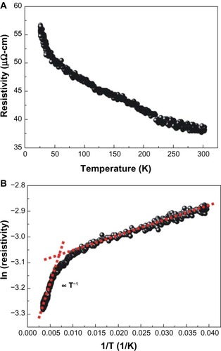
Clearly, there is a rapid increasing trend with the decrease in temperature, especially below 50 K. This represents a negative TCR (dp/dT < 0) phenomenon that cannot be explained by semiclassical theory. seems to imply that there would need to be two models to handle the variable trends of TCR with a transient point.
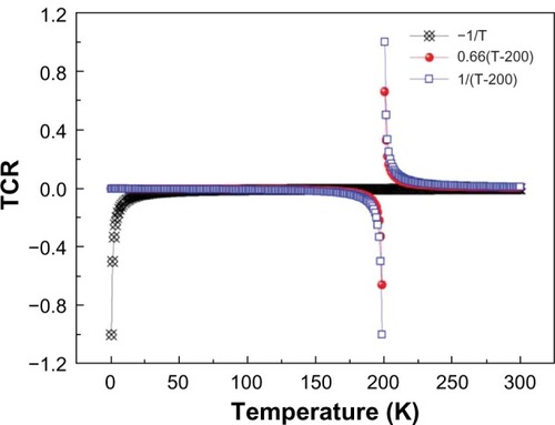
Other researchers have had similar results. Sheng reported that, for high-resistivity granular disordered systems, low-field conductivity exp(−A/Tα) with α = 1/2 is obeyed over large temperature ranges, with possible crossovers to α = 1/4 at low temperatures and to α > 1/2 at high temperatures.Citation25 The temperatures at which the crossovers occur depends on the distribution of grain size. As shown in , Naeemi reported that, for single-wall and few-wall CNTs, the TCR reaches 1/(T-200K) for lengths much larger than the electron MFP.Citation11 For MWCNTs with a large diameter (>20 nm), TCR varies from −1/T to +0.66/(T-200K) as the length varies from zero to very large values. There exists a “singular point” around 200 K and a separate fitting model in two parts. The results were derived by simulations and assumed the body of the object would be perfect. However, what is different in a real MWCNT body which has multiple defects?
Figure 3 The work graph of Naeemi.Citation11 Based on the physical and equivalent circuit model of carbon nanotubes, the temperature coefficient of resistance is always positive and increases with length. For single- and few-wall carbon nanotubes, it reaches 1/(T-200K) for lengths much larger than the mean free path. For multiwalled carbon nanotubes with a large diameter (>20 nm), the temperature coefficient of resistance varies from −1/T to +0.66/(T-200K) as the length varies from zero to very large values.
In our work, we employed hopping conductivity and variable range hopping conductivity theories to fit the experimental results for the two different slopes of .
In the hopping conductivity mechanism, the variation of resistivity at relatively high temperatures is in proportion to the Boltzman factor, exp(−ε/kT). Hopping conductivity theory, σ = σminexp (−ε/kT), was used, as shown in , to display the fitting result curve. The resistivity σminderived from the fitting curve is 38 μΩ-cm, and the corresponding activation energy ε is 4.46 meV, which is quite close to the energy gap of SWCNT.Citation26 Therefore, as the temperature increases, the thermal energy will excite an electron from the valance band to the conduction band, which leads to high conductivity.
Figure 4 The fitting curve contrasted with real experimental data of a multiwalled carbon nanotube where curve (a) is obtained from hopping conductivity theory, curve (b) is obtained from variable range hopping theory, and curve (c) is the combined hopping conductivity and variable range hopping theories for the temperature dependence of resistivity.
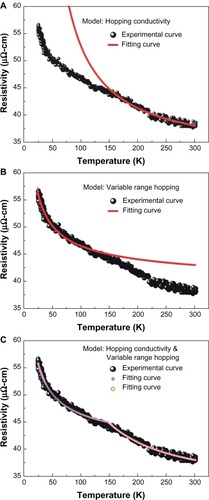
However, the TCR at low temperature ranges cannot be explained by the exponential law above. Instead, when using strong localization theory (kf 10 ~ 1), variable range hopping may prevail at low temperatures, as shown in . The exact variable range hopping theory that describes the low-temperature behavior of resistivity in strongly disordered systems, where states are localized, can be expressed as:
where Rav is the average hopping distance, N(εF) is the density of state, vph is the coefficient according to the phonon spectrum, B is the coefficient related to the density of state, and d indicates the dimension.
Combining these two models, we can cover the temperature range from high to low (300–25 K), and note that there exists a singular point around 150 K (which is 50 K lower than in the work plot of Naeemi in ).Citation11 This well-matched result is shown in , and explained by taking into account the combined equations of hopping conductivity and variable range hopping conductivity theory. The fitting results are shown in , and are very consistent with Mott’s predictions for the conductivity of amorphous materials.Citation18
Table 1 The parameters obtained for fitting with hopping conductivity and variable range hopping models for a single multiwalled carbon nanotube
The meaning of the singular point here was presumed to be a transient point that governs the conditional change from inelastic to elastic collisions, ie, a measure of the temperature above which more modes of phonons in MWCNTs will be excited. To recognize and describe this unique property of MWCNTs, we named this singular point the “Lue point” temperature.
For comparison purposes, the grain boundary scattering model was also employed to fit for resistivity versus temperature in our individual MWCNT. The best fitting result is shown as a solid line in , and makes the physical constraints of Equationequation (6)(6) with p = 1 and Tg <1.
Figure 5 The fitting curve is obtained from grain boundary scattering theory and compared with real experimental data of an individual multiwalled carbon nanotube.
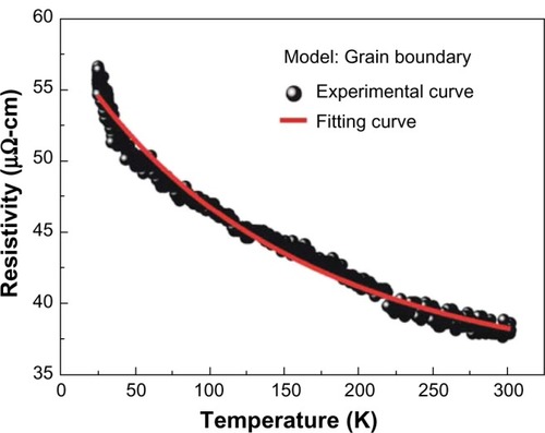
In general, the value of p depends on the dominant inelastic scattering mechanism, and is presumed to be fixed in the 0.5–4.0 temperature range.Citation27 The parameters obtained by fitting the R-T curves with the least square errors method are listed in . The parameter term, lo/RG, indicates that the electrons are scattered by lo/RG barriers in one mean free path (lo) where RG is the interval between grains. According to the scanning electron microscopy image shown in , the diameter of the MWCNT is smaller than approximately 100 nm, with about 2.3 nm/per layer, therefore the elastic mean free path obtained by the fitting result of grain boundary scattering model is around 3–4 nm.
Table 2 The parameters obtained for best fitting with grain boundary scattering model for a multiwalled carbon nanotube
Parameter b plays a crucial role and affects the tendency of the R-T curve, due to the mean free path’s l (T) = lo/(1 + bTp) variance with temperature. According to Matthiessen’s rule, 1/l(T) = 1/lo+1/lin, where lin is the mean free path due to the inelastic scattering which comes from the contribution of the optical phonon, we deduce that the interaction between the phonon and electron at low temperatures is small, ie, the inelastic mean free path varying with temperature causes the negative TCR characteristic in our study. In addition, the electron transmission probability, Tg, for electrons to pass a single grain boundary is in the order of 10−1, as derived from the fitting result.
Conclusion
In this study, we have produced an individual MWCNT across electrodes by a method of MPECVD and measured the temperature dependence resistivity of this MWCNT to investigate its electronic properties.
For comparison, the effect of quantum confinement (strong localization) and grain boundary theories were quoted to explain the anomalous resistivity (a negative TCR characteristic). With regard to strong localization, the fitting result can be obtained by combining hopping conductivity theory in the high-temperature range and variable range hopping conductivity theory at the low-temperature range. The most appropriate fitting result is accomplished by using grain boundary theory. The singular “Lue point” temperature can be successfully described as a unique property of MWCNTs. The nanosize of the fabricated MWCNTs ensures the validity of the grain boundary scattering model and the temperature-related inelastic mean free path dominates the R-T curve, causing the negative TCR characteristic.
Acknowledgments
This work was supported by the National Science Council of the Republic of China under the contracts NSC-986-2112-M007 and NSC 97-2221-E-029-007-.
Disclosure
The authors report no conflict of interest in this work.
References
- LiJYeQCassellABottom-up approach for carbon nanotube interconnectsAppl Phys Lett20038224912493
- SaitoRDresselhausGDresselhausMSPhysical Properties of Carbon Nanotubes5th edSingaporeImperial College Press2003
- AnantramMPLéonardFPhysics of carbon nanotube electronic devicesRep Prog Phys200669507561
- KoentoppMChangCBurkeKCarRDensity functional calculations of nanoscale conductanceJ Phys Condens Matter200820083203
- RibayaBPLeungJBrownPRahmanMNguyenCVA study on the mechanical and electrical reliability of individual carbon nanotube field emission cathodesNanotechnology20081918520121825685
- IijimaSBrabecCMaitiABernholcJStructural flexibility of carbon nanotubesJ Chem Phys199610420892092
- ChangLWLueJTElectrical conductance in a single carbon wireJ Nanosci Nanotechnol2005515
- ChenSYMiaoHYLueJTOuyangMSFabrication and field emission properties of multiwall nanotubesJ Phys D Appl Phys200437273279
- LiangWBockrathMBozovicDHafnerJHTinkhamMParkHFabry-Perot interference in a nanotube electron waveguideNature200141166566911395762
- FrankSPoncharalPWangZLHeerWACarbon nanotube quantum resistorsScience1998280174417469624050
- NaeemiAMeindlJDPhysical modeling of temperature coefficient of resistance for single- and multi-wall carbon nanotube interconnectsIEEE Electron Device Letters2007282135138
- AndoTMatsumuraHNakanishiTTheory of ballistic transport in carbon nanotubesPhysica B20023234450
- MiyamotoYRubioABerberSYoonMTomanekDSpectroscopic characterization of Stone-Wales defects in nanotubesPhys Rev B200469121413(R)
- PopEMannDReifenbergJGoodsonKDaiHElectro-thermal transport in metallic single-wall carbon nanotubes for interconnect applicationsIEDM Technical Digest2005253
- SvizhenkoAAnantramMPGovindanTRBallistic transport and electrostatics in metallic carbon nanotubesIEEE Transactions on Nanotechnology20054557562
- ChenSYChangLWPengCWMiaoHYLueJTGrowth of carbon nanotubes at low powers by impedance-matched microwave plasma enhanced chemical vapor deposition methodJ Nanosci Nanotechnol200551887189216433426
- WangYSantiago-AvilésJJLarge negative magnetoresistance and strong location in highly disordered electrospun pregraphitic carbon nanofiberAppl Phys Lett200689123119
- MottNFDavisEAElectronic Processes in Non-Crystalline Materials2nd edOxfordClarendon Press1979
- GodetCVariable range hopping revisited: The case of an exponential distribution of localized statesJ Non-Cryst Solids2002299–302333338
- MayadasAFShatzkesMElectrical-resistivity model for polycrystalline films: The case of arbitrary reflection at external surfacesPhys Rev B1970113821389
- VanceaJHoffmannHKastnerKMean free path and effective density of conduction electrons in polycrystalline metal filmsThin Solid Films1984121201
- ChenLJTyanJHLueJTThe non-metallic conductivity of NbGe films sputtered on silicon substratesJ Phys Chem Solids199455871879
- JayannavarAMKumarNMooij correlation in disordered metalsPhys Rev B1988371573576
- DaouRNicolasDLLeBoeufDLinear temperature dependence of resistivity and change in the Fermi surface at the pseudogap critical point of a high-Tc superconductorNature Phys200953134
- ShengPKlafterJHopping conductivity in granular disordered systemsPhys Rev B19832725832586
- IshibashiKMoriyamaSFuseTYamaguchiTCarbon nanotubes as building blocks of quantum dotsPhysica E200635338343
- GiordanoNExperimental study of localization in thin wiresPhys Rev B19802256355655