

ABSTRACT
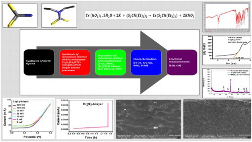
Current investigation has for the first time synthesized chromium sulphide diethyldithiocarbamate [Cr2S3(Et2DTC)] complex utilizing diethyldithiocarbamate (DDTC) utilizing single source precursor method. Thin films of bilayer chromium sulphide diethyldithiocarmate and molybdenum disulphide [Cr2S3-MoS2(Et2DTC)] were deposited on the fluorine doped tin oxide (FTO) substrate by physical vapour deposition (PVD). Synthesized complex and bilayer were characterized by Xray powder diffraction (XRD), Fourier transform infrared spectroscopy (FT-IR), ultraviolet-visible spectrophotometry (UV-Vis), and scanning electron microscopy (SEM) for exploration of the compositional, optical, crystalline and morphological parameters, respectively. FT-IR peaks expressed the chelation of [Cr2S3(Et2DTC)] expressing interactions between chromium sulphide and the ligand. The band gaps obtained from Tauc plot were 3.89 (direct) and 3.38 eV (indirect), respectively for Cr2S3(Et2DTC) complex. The direct and indirect band gap of 3.75 and 3.35 eV, respectively, were obtained for [Cr2S3-MoS2(Et2DTC)] bilayer thin films. Average crystallite size of 13 (hexagonal orientation) and 13.4 (orthorhombic orientation) nm and for Cr2S3(Et2DTC) complex and [Cr2S3-MoS2(Et2DTC)] bilayer thin films expressed from XRD. SEM micrographs expressed cannular and rod protrusions for Cr2S3-DDTC complex and smoother and unvarnished surficial characteristics for [Cr2S3-MoS2(Et2DTC)] bilayer thin films corresponding to compactness and uniformity of the films. Furthermore, [Cr2S3-MoS2(Et2DTC)] also expressed remarkable electrochemical aspects of the current generation and operational stability of analysed through 5760 s at 100 mA analysed via linear sweep voltammetry and chronoamperometry. The fabricated films can be efficiently used in optoelectronic devices. Current work can be extended to the optimization of bilayer thin films fabrication for achieving an alleviation in the band gaps.
GRAPHICAL ABSTRACT
Acknowledgements
Authors acknowledge Fatima Jinnah Women University, Pakistan, for providing all research facilities; National Centre for Physics, Pakistan for PVD films deposition; School of Natural Sciences, National University of Science and Technology, Pakistan, for LSV and chronoamperometric measurements and Institute of Space Technology, Pakistan, for XRD and SEM analysis.
Disclosure statement
No potential conflict of interest was reported by the authors.