
 ?Mathematical formulae have been encoded as MathML and are displayed in this HTML version using MathJax in order to improve their display. Uncheck the box to turn MathJax off. This feature requires Javascript. Click on a formula to zoom.
Abstract
This article presents research on a new solution for industrial helmets improving mechanical and physical properties (temperature resistance and reflection of infrared radiation). The application of known technology in a new personal protective equipment area has been described in order to increase their level of safety and comfort of use. In this work we have studied the effect of a selected magnetron sputtering coating method onto polymer substrates, such as acrylonitrile–butadiene–styrene copolymer, polycarbonate, polyethylene, high-density polyethylene, polyamide, glass and silicon. Coatings made of copper, aluminium, TiN and TiAl were used. This work aims at identifying the best substrates for coating deposition improving the quality of protective helmets. On the basis of the obtained results, it can be stated that the TiN coating provides the best protection from infrared radiation and the best scratch resistance.
1. Introduction
Many workplaces, especially in the sectors of metallurgy, power engineering and founding, but also in the emergency services, are exposed to hazards associated with thermal radiation of high intensity. In such places, the currently used head protection equipment very often fails to provide adequate protection in the form of thermal insulation. In addition, industrial helmets subjected to infrared radiation lose their critical protective properties such as shock absorption ability, or puncture resistance, and the users begin to feel tired more quickly. Currently, a single reflective metal layer is frequently used in head protection. Coatings of this type are often produced using physical vapour deposition (PVD) methods [Citation1–3]. It is also possible to apply a coating consisting of many components, which may be either a gradient or stratified in character [Citation4–8]. The application of this technology poses challenges associated mainly with the substrate material. In the case of protective helmets, these are mostly plastics which should be processed at a temperature below 100 °C. For this reason, among others, magnetron sputtering has been selected as the coating method [Citation9,Citation10].
Modern technology allows the design and manufacture of thin nanocrystalline coatings according to assumed parameters. The vacuum-plasma technologies used for this purpose enable the development of modern, sophisticated personal protective equipment (PPE) to ensure improved protection of the user's head without increasing the weight of the equipment at the same time.
One of the modern methods of surface modification used in the production of specialized tools and demanding engineering structures, as well as in medical devices and optical technology, is technology including PVD methods. One of these methods, magnetron sputtering [Citation11–14], allows the deposition of layers onto plastic substrates at a temperature below 100 °C.
To this end, CIOP-PIB's Department of Personal Protective Equipment had undertaken a research project aimed at the development of modern coatings reflecting and blocking infrared radiation, which also have high mechanical properties in terms of hardness, adhesion and resistance to oxidation. Such features are necessary in the case of heavy-duty head protection equipment used, e.g., by steelworkers, foundry staff, emergency services, firemen, etc. This article presents the assessment of technological potential in this area, together with the results concerning the selected properties of protective coatings on plastic substrates.
The novelty presented in this work is the application of the well-known technology of applying thin coatings, and its adaptation to the area of industrial protective helmets.
2. Methods and materials
2.1 Selection and preparation of substrates for coating deposition
The most popular plastics used for the production of helmet shells and face shields include acrylonitrile–butadiene–styrene copolymer (ABS), polycarbonate (PC), polyethylene (PE) and high-density polyethylene (HDPE) as well as polyamide (PA) [Citation15,Citation16]. For this reason, it was decided to choose substrate samples made from each of these materials. The specificity of the planned research (optical studies) resulted also in the necessity to use two additional substrates – glass and monocrystalline silicon. The plastic samples of 7 cm × 7 cm dimensions were cut directly from the helmet shells. Microscope slides were used as glass samples, and silicon wafers as silicon samples. The surface area of the produced samples ranged from 1 to 6 cm2.
Due to the different mechanical properties and chemical resistance of the samples, two different methods for their preparation were developed. Treatments associated with preparation of the surface prior to deposition of coatings aimed at attaining their better adhesion to the substrate. Therefore, before each process, the PE, PC and PA styrene copolymer substrates were washed in a detergent and hot water. Subsequently, all of the substrates were dried with a filtered air flow. Such a method of surface preparation did not affect negatively the condition of the substrates and allowed maximum adhesion of the applied coating.
Glass substrates and monocrystalline silicon were washed in acetone using an ultrasonic cleaner. The times for such treatment were selected experimentally and usually amounted to several minutes, as the impact of ultrasonic cavitation erosion may affect the surface morphology. The ultimate removal of trace impurities was obtained by heating for a period of 1 h in residual vacuum (10−2 Pa), followed by purification by ion sputtering in glow discharge plasma for desorption of gases incorporated into the surface, or removal of residual oxide layers left over from the previous treatments.
The process of preparing the sample surface for deposition of coatings was carried out immediately before deposition in each case. The samples prepared for coating were mounted in special holders in the vacuum chamber of the thin film deposition stands. The handles were constructed in such a way as not to cover the area designed for coating application and at the same time to allow collision-free movement of the sample suspended on the rotary table.
2.2 Selection and characterization of the coating method and apparatus
Magnetron sputtering was selected as the method to be used for coating deposition. This technology allows the processes to be carried out using reactive gas mixtures containing carbon or nitrogen and separate power control for each of the magnetron sources located in the vacuum chamber. This allows virtually any chemical composition of the coating material. Magnetron technology does not make it possible to achieve such power of the processes, and thus such mechanical properties of coatings as arc technologies, but thanks to this the energy of the process is not high. This allows deposition of the coatings at temperatures below 100 °C, which makes it possible to use plastic materials as substrates, while keeping high mechanical properties, adequate for coatings protecting against infrared radiation.
To produce the layers, a B-901 device (Hochvakuum, Germany) (Figure ) installed at Lodz University of Technology's Institute of Materials Science and Engineering was used. Its chamber is equipped with four independent WK-100 magnetrons (Dora, Poland) supplied by separate power sources. It consists of two main units: a vacuum chamber and a pumping system.
Figure 1. Schematic drawing of the B901 device (Hochvakuum, Germany) vacuum chamber.
Note: 1 = mass flow controller; 2 = shut-off valves; 3 = vacuum gauge head; 4 = table rotation engine; 5 = vacuum line connecting the chamber with a high vacuum system; 6 = flap gauge; 7 = infrared radiator for load heating; 8 = rotary table; 9 = working chamber with Ø 900 mm × 900 mm dimensions made of austenitic steel; 10 = polarization (negative) of the table with samples; 11 = water cooling of the magnetron discs; 12 = electric power supply to the magnetrons; 13 = substrates for coating deposition; 14, 15 = magnetrons; 16 = working gas flow; Ar =argon.
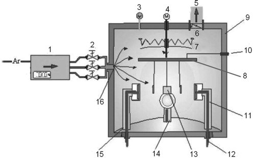
In addition to the magnetrons, the chamber is equipped with probes to measure the initial and high vacuum, sight glasses, a rotary table for mounting substrates and flowmeters to control gas flow rates. It is also possible to clean the surface of the samples in glow discharge plasma using a specialized power supply unit to induce a glow discharge.
During the synthesis, the table with pendant samples can be polarized with a potential of −50 V, and it can rotate around the vertical axis of the vacuum chamber with an angular speed of approximately 0.3 rad s−1, which allows for uniform deposition. The process temperature is measured by thermocouples placed inside the chamber and connected to a millivoltmeter outside the chamber.
2.3 Selection of coating deposition process parameters
In each case, the synthesis of coatings on the selected substrates is associated with the selection of process parameters. The power of magnetron discs, the working pressure in the chamber, the gas flows and the deposition time were set so as not to exceed the process temperature of 100 °C.
It was assumed that coatings with defined chemical composition and thickness, scheduled to be 1.7 ± 0.5 μm, will be obtained. Therefore, the chemical composition, thickness and adhesion were measured after each process. The obtained results enabled correction of the deposition parameters during the next synthesis. The final selection of deposition parameters is presented in Table .
Table 1. Deposition parameters.
Deposition of TiN coatings was preceded by spraying pure titanium without the presence of nitrogen for 300 s. After that time, nitrogen was introduced gradually into the vacuum chamber up to 6.6% at a flow rate of 50 sccm, to obtain the desired TiN coating. TiAl coatings were deposited using one magnetron as a TiAl alloy with 50/50% atomic ratio was used as a target.
After each process, the magnetron power supply was turned off and flow of the working gas into the vacuum chamber was cut off. The coated samples remained in the vacuum chamber for a few hours, after which the chamber was aerated and the samples were taken out.
3. Results of the parameter determination
3.1 Coating thickness
Coating thickness was determined using cross-sectional imaging of samples made on silicon substrates. Scanning electron microscopy (SEM) (S-3000N; Hitachi, Japan) was used in this case. Examples of SEM images of individual coatings deposited on monocrystalline silicon substrates are shown in Figures –. The thickness was measured five times at different cross-section locations, and the means calculated from the obtained results are presented in Table .
Figure 2. Cross-section of monocrystalline silicon substrate coated with aluminium.
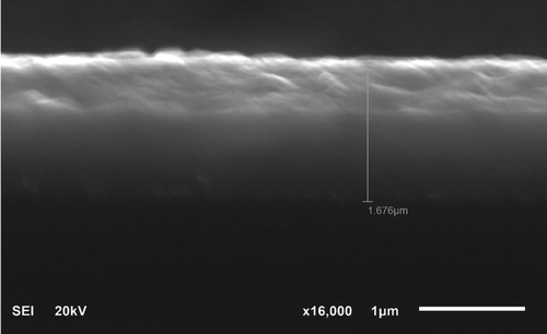
Figure 3. Cross-section of monocrystalline silicon substrate coated with copper.
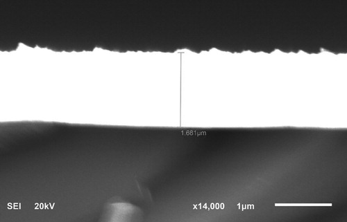
Figure 4. Cross-section of monocrystalline silicon substrate coated with TiAl.
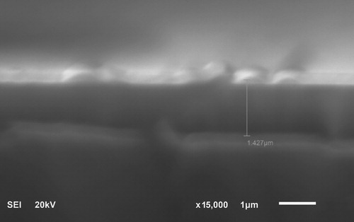
Figure 5. Cross-section of monocrystalline silicon substrate coated with TiN.
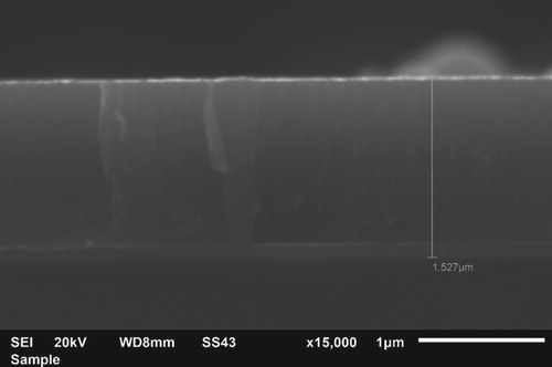
Table 2. Coating thickness.
The desired coating thickness was achieved in each case. This allows the other intended parameters of the coating such as infrared radiation reflectivity, hardness and adhesion to be obtained. Coatings of greater thickness may be subject to cracking and peeling due to the magnitude of internal stresses in the layers. Reducing such stresses, e.g., by annealing, is not possible due to the substrate material which is not resistant to elevated temperatures.
3.2 Chemical composition
Studies of the TiN coating were conducted using an Hitachi 3000N with Thermo–Noran System (Thermo Fisher Scientific, USA) scanning microscope [Citation17,Citation18] with an attachment [Citation19] manufactured by EDS (Noran Instruments USA). The results obtained for the TiN coating are presented in Table .
Table 3. Results concerning the chemical composition of TiN.
The presented result for the chemical composition of TiN shows a negligible content of other elements that should not be there considering the constituent elements of the coating itself. This fact is due to the method of analysis energy dispersive spectroscopy (EDS) and the relatively small thickness of the studied coating. It contains elements of small mass numbers, which are characterized by low absorption of electrons. A characteristic feature of PVD processes is that the coating and the substrate itself may contain small amounts of other elements. During the investigation of the chemical composition, the primary electron beam from the cathode of the scanning electron microscope also induced electron transitions in oxygen and argon atoms.
The results concerning the chemical composition of TiN show approximately 55% titanium and 45% nitrogen content, respectively. According to the information found in the literature, such values allow positive verification of the coating. In order to characterize its other properties and evaluate its suitability for use on head protection equipment, parameters such as hardness and adhesion will be determined in further research.
The chemical composition was not studied in the case of mononuclear aluminium and copper coatings, as well as TiAl. They were synthesized, respectively, from aluminium and copper targets, and the target with chemical composition 50% titanium, 50% aluminium. The chemical composition of coatings obtained as a result of magnetron sputtering processes conducted without reactive gases is identical to the chemical composition of the used targets.
3.3 Microhardness
Microhardness measurements according to the Vickers method [Citation20] on the HV0.01 scale were performed using a FH-1 device (Future-Tech, Japan). Each coating on each substrate was measured five times. The average microhardness value for each substrate is presented in Table .
Table.4. Average values of microhardness for each surface.
The highest microhardness values were obtained for the TiN coating on all surfaces. Additionally, the highest hardness of each of the coatings was obtained on the PC substrate. This material is the hardest among all those studied and therefore the thin coating layer underwent the slightest deformation during the test. It is noteworthy that all of the obtained results are characterized by a considerable standard deviation. This is mainly due to the very low hardness of the substrate. In addition, the test specimens were not completely flat and were characterized by a curvature of the surface face on which the measurements of the impressions were performed. Due to their properties, compressed plastics demonstrated an elastic reaction of the substrate.
3.4 Adhesion of coatings to the substrate
The hardness and stiffness of the used substrates were too low to enable a reliable measurement of adhesion by the scratch test (Lodz University of Technology, Poland). As demonstrated by the tests, the substrate underwent significant plastic deformation after application of the load and after the linear movement of the diamond penetrator in a direction parallel to the substrate surface. Instead of scratching the surface of the sample with the coating, destruction of the soft substrate occurred, even after application of a load of approximately 100 g.
Therefore, the Daimler-Benz method was used to assess the quality of adhesion. This test involves measuring hardness with the Rockwell method on the C scale. The test is based on identifying damage to the coating within the impression area after the measurement of hardness and comparing this with patterns on the 6-point hydrogen fluoride (HF) scale (where HF-1 = best quality, HF-6 = worst quality). Due to the large diameter of the impression in the soft substrate material after the Daimler-Benz test, even when taking photographs at the lowest possible magnification, i.e., 50×, the pictures show only selected fragments of impressions. The sample images of impressions obtained in the Daimler-Benz test, taken under the microscope at 50× magnification, are presented in Table .
Table 5. Sample results for measuring the quality of adhesion in the form of impression images taken under the microscope at 50× magnification on the HF scale.
The adhesion testing method used showed that the highest quality of adhesion (HF-1) was achieved for all coatings on all substrates. On this basis, it can be concluded that the deposition process parameters and the method of substrate preparation were correct.
The presented results concerning the basic parameters of the layers clearly indicate that they can be used as coatings applied onto helmets to protect against infrared radiation.
3.5 Optical studies
Optical studies were performed in a Cary 5000 spectrophotometer (Varian, Australia). This method allows determination of the transmittance–reflectivity properties of optical radiation within the infrared spectrum for samples of materials, with no need to examine the complete product. The results obtained made it possible to verify the prepared coatings for their effectiveness in the reflection of infrared radiation.
For the measurement of spectral characteristics of reflection (R(λ)), the ratio of the reflected flux (ΦR) to the incident measuring beam (Φ0) is determined for a particular wavelength. Spectral reflectivity (RF(λ)) is expressed by the general equation:
(1)
(1)
where RF(λ) = spectral reflectivity; ΦR = reflected flux; Φ0 = incident measuring beam.
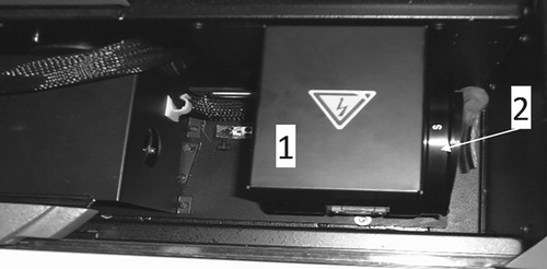
In the case of measurement of the spectral reflectivity characteristics, the measurement geometry utilizing an integrating sphere, which allows measurement of the total radiation reflected and scattered from the surface of the sample, should be used. Figure shows photographs of the Cary 5000 spectrophotometer chamber with a mounted test sample.
Figure 6. The spectrophotometer chamber with the test sample for which the spectral characteristic of reflection (R(λ)) was measured.
Note: 1 = integrating sphere; 2 = test sample.
To characterize the reflection parameters, the average spectral reflectivity of an infrared wavelength range of 780–2000 nm was used. This was determined from the following equation:
(2)
(2)
where R = mean spectral reflectivity of infrared for the 780–2000 nm wavelength range; 1/1220 nm = factor introduced for the average reflectivity value considering the value of the measuring step in the spectrophotometric study, which is 1 nm; R(λ) = reflection; λ = wavelength.
Optic studies were conducted for all of the produced layers to determine the reflection coefficient [Citation21]. Tests were performed for the coatings deposited on substrates made of glass and monocrystalline silicon. Figure shows the correlations of relative reflectivity with wavelength obtained in the tests performed on aluminium, copper, TiN and TiAl coatings. On the basis of the known characteristics, the mean reflectivity values were determined. The results are shown in Figure .
Figure 7. Correlation of infrared reflectance (R) with wavelength.
Note: Al = aluminium; Cu = copper.
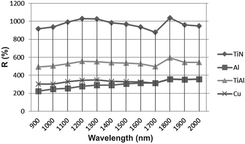
Figure 8. Average relative values of infrared reflectivity.
Note: Al = aluminium; Cu = copper.
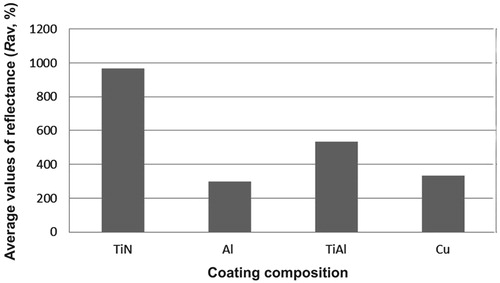
Comparison of the determined average reflectivity value for the test samples may indicate which coating reflects most infrared radiation, on average, over the 780–2000 nm range. As can be seen clearly from Figure , the sample with the TiN coating has the highest average value of infrared reflection. It is more than three times higher than for the aluminium coating. Moreover, a layer made of TiAl compared with aluminium and copper coatings demonstrates almost twice the average value of infrared reflection. In terms of the infrared radiation-reflecting properties, the TiN coating is definitely the most effective.
Due to the approximately 1.5-µm thickness of the coatings, light transmission was not studied at this stage because coatings of such thickness are impervious to radiation.
4. Conclusions
In the research, the possibility of improving the properties of polymeric materials used in the construction of protective helmets by thin-film coating was verified. Coatings made of copper, aluminium, TiN and TiAl were deposited on substrates made of ABS, HDPE, PC and PA materials by magnetron sputtering. Such a new solution improves their level of safety and increases the comfort of use.
Initially, the thickness and chemical composition of the coatings were verified. Then, the microhardness test was conducted and adhesion properties were measured. The final stage of the study was to evaluate the reflective optical properties of the samples (infrared reflectivity).
It has been stated that the TiN coating provides potentially the best protection against infrared radiation which can be used on plastic surfaces. It has the highest hardness and ability to reflect radiation from all tested coatings. Moreover, its adhesion to the substrate does not differ from the adhesion of other coatings. Owing to the presence of protective coatings, the helmet shell will absorb less energy and will not be heated to an extent posing the risk of a loss of its mechanical strength and shock absorption ability. Reducing energy absorption is also associated with limiting the temperature rise under the helmet, resulting in improving the user's comfort.
The obtained results will make it possible to continue research into the application of the selected coatings onto samples a few dozen square centimetres in size, as well as models of protective equipment.
Disclosure statement
No potential conflict of interest was reported by the author.
ORCID
Marcin Jachowicz http://orcid.org/0000-0002-6402-6897
Additional information
Funding
Related Research Data
References
- Miernik K. Podstawy fizyczne rozpylania magnetronowego. Inżynieria Powierzchni [Physical bases of magnetron sputtering]. Surf Eng. 1996;1:66–74. Polish.
- Kula P. Inżynieria warstwy wierzchniej [Engineering the surface layer]. In: Tadeusiewicz M, editor. Łódź: Wydawnictwo Politechniki Łódzkiej; 2000. Polish.
- Ledermann N, Baborowski J, Muralt P, et al. Sputtered silicon carbide thin films as protective coating for MEMS applications. Surf Coat Technol. 2000;125:246–250. doi: 10.1016/S0257-8972(99)00568-X
- Wendler B., Danielewski M., Przybylski K., et al. New type AlMo-, AlTi- or Si-based magnetron sputtered protective coatings on metallic substrates. Journal of Achievements in Materials and Manufacturing Engineering. 2003; Vol. 12; p. 1033–1040.
- Wendler, B., Jachowicz, M., Karolus, M., et al. Powłoki ochronne SiC, SiCN, SiN na stopach metali osadzane reakcyjną metodą magnetronową przy niskich temperaturach. Inżynieria Materiałowa [Material Engineering] Warszawa: SIGMA-NOT; 2006; Vol. 27; no. 3; p. 551–553. Polish.
- Wendler, B., Rylska D., Rylski A., et al. Powłoki ochronne na stopach metali osadzane metodami PVD. Inżynieria Powierzchni [Surface Engineering] Warszawa; Institute of Precision Mechanics; 2005; no. 2; p. 14–18. Polish.
- Wendler B, Jachowicz M, Kaczmarek Ł, et al. Si-based protective coating on Si and steel substrates. Inżynieria Materiałowa [Material Engineering] Warszawa: SIGMA-NOT; 2004; R. XXV; no. 3; p. 673–675.
- Wendler B, Kaczmarek Ł, Jachowicz M, et al. Oxidation resistant coatings on gamma - TiAl alloy. Inżynieria Materiałowa [Material Engineering] Warszawa: SIGMA-NOT; 2004; R. XXV; no. 3; p. 677–680.
- Miernik K. Działanie i budowa magnetronowych urządzeń rozpylających. [The operation and construction of the magnetron sputtering device]. Biblioteka Problemów Eksploatacji. Radom. 1997. Polish.
- AGC-Plasma Technology Solutions; [cited 2020 April 19]. Available from: https://www.agc-plasma.com/technologies/#magnetron-sputtering-equipment.
- Kelly P, Arnell RD. Magnetron sputtering: a review of recent developments and applications. Vacuum. 2000;56(3):159–172. doi: 10.1016/S0042-207X(99)00189-X
- Greene JE. Tracing the recorded history of thin-film sputter deposition: from the 1800s to 2017. J Vac Sci Technol A. 2017;35(5):05C204. doi: 10.1116/1.4998940
- Chen Y, Yang J, Cheng S, et al. Structural investigation of ZnO:Al films deposited on the Si substrates by radio frequency magnetron sputtering. Thin Solid Films. 2013;545:183–187. doi: 10.1016/j.tsf.2013.07.079
- Pat S, Mohammadigharehbagh R, Özen S, et al. The Al doping effect on the surface, optical, electrical and nanomechanical properties of the ZnO and AZO thin films prepared by RF sputtering technique. Vac. 2017;141:210–215. doi: 10.1016/j.vacuum.2017.04.025
- Kumar Kar S, Anshuman DA, Raj H, et al. New design and fabrication of smart helmet. IOP Conf. Series: Materials Science and Engineering 402; IOP Publishing; 2018; 012055; p.1–10.
- Palmer SB. Single use crash helmets: does material density affect peak G [master's thesis]. Sacramento (CA): California State University, Sacramento; 2016. Available from: https://csus-dspace.calstate.edu/bitstream/handle/10211.3/171154/%20Stephanie_Palmer_Final_Thesis.pdf?sequence=1
- Barbacki A. Mikroskopia elektronowa [Electron microscopy]; Wydawnictwo Politechniki Poznańskiej; 2007; Poznań. Polish.
- Słowik G. Podstawy mikroskopii elektronowej i jej wybrane zastosowania w charakterystyce katalizatorów nośnikowych [Fundamentals of electron microscopy and the selected application the characteristics of the catalyst carrier]. Rzeszów: Uniwersytet Rzeszowski; 2012. ISBN: 978-83-931292-8-7. Polish.
- Szumer A. Podstawy ilościowej mikroanalizy rentgenowskiej [Fundamentals of quantitative X-ray microanalysis]. Warszawa: WNT; 1994. Polish.
- European Committee for Standardization (CEN). Metallic materials – Vickers hardness test – Part 1: Test method. Brussels: CEN; 2005. Standard No. EN ISO 6507-1:2005.
- Owczarek G, Jurowski P. Zmiany transmisji promieniowania optycznego przez soczewki wewnątrzgałkowe eksplantowane z powodu zjawiska glisteningu, [Changes in transmission of optical radiation through intraocular lenses explanted due to the phenomenon of glistening]; Warszawa; Prace Instytutu Elektrotechniki; 2012; Vol. 255; p. 201–211. Polish.