
 ?Mathematical formulae have been encoded as MathML and are displayed in this HTML version using MathJax in order to improve their display. Uncheck the box to turn MathJax off. This feature requires Javascript. Click on a formula to zoom.
Abstract
A new materials group to implement dense wavelength division multiplexing (DWDM) in Si photonics is proposed. A large thermo-optic (TO) coefficient of Si malfunctions multiplexer/demultiplexer (MUX/DEMUX) on a chip under thermal fluctuation, and thus DWDM implementation, has been one of the most challenging targets in Si photonics. The present study specifies an optical materials group for DWDM by a systematic survey of their TO coefficients and refractive indices. The group is classified as mid-index contrast optics (MiDex) materials, and non-stoichiometric silicon nitride (SiNx) is chosen to demonstrate its significant thermal stability. The TO coefficient of non-stoichiometric SiNx is precisely measured in the temperature range 24–76 °C using the SiNx rings prepared by two methods: chemical vapor deposition (CVD) and physical vapor deposition (PVD). The CVD-SiNx ring reveals nearly the same TO coefficient reported for stoichiometric CVD-Si3N4, while the value for the PVD-SiNx ring is slightly higher. Both SiNx rings lock their resonance frequencies within 100 GHz in this temperature range. Since CVD-SiNx needs a high temperature annealing to reduce N–H bond absorption, it is concluded that PVD-SiNx is suited as a MiDex material introduced in the CMOS back-end-of-line. Further stabilization is required, considering the crosstalk between two channels; a ‘silicone’ polymer is employed to compensate for the temperature fluctuation using its negative TO coefficient, called athermalization. This demonstrates that the resonance of these SiNx rings is locked within 50 GHz at the same temperature range in the wavelength range 1460–1620 nm (the so-called S, C, and L bands in optical fiber communication networks). A further survey on the MiDex materials strongly suggests that Al2O3, Ga2O3 Ta2O5, HfO2 and their alloys should provide even more stable platforms for DWDM implementation in MiDex photonics. It is discussed that the MiDex photonics will find various applications such as medical and environmental sensing and in-vehicle data-communication.
1. Introduction
Si photonics enables cost-effective wide-bandwidth communication and computation networks, and will shortly appear in data centers and in our daily life [Citation1–7]. The figure of merit (FoM) of a network system is given by . The question of why Si photonics is preferable to Si electronics can be answered by considering optical fiber communication. Figure shows progress in information capacity [Citation8]. Starting with voice communication between Bell and Watson through their telephone demonstration between Boston and Cambridge in 1875, there was exponential increase in information capacity by five orders of magnitude in nearly 100 years due to ‘electrical’ communication (red circles). There is a large jump in 1980 brought about by optical fiber communication. This technology instantaneously increased information capacity by three orders of magnitude, much faster than was possible by the previous technology. The green squares in Figure signify that 100 colors of light were used to communicate (green squares), which increased the information capacity by 100 times compared with using one color (blue triangles). Wavelength division multiplexing (WDM) is very important in optical communication. The fundamental device is a prism filter besides light emitters and detector, which is called multiplexing/demultiplexing (MUX/DEMUX). The International Telecommunication Union – Telecommunication Standardization Sector (ITU-T) recommends the following protocol for WDM: the difference in wavelength between colors of light, i.e. channel spacing, should be 100 GHz (0.8 nm), with a crosstalk lower than –30 dB in the wavelength range near 1.55 μm. This is referred to as dense WDM (DWDM). This is the requirement to MUX/DEMUX as well as light emitter. Despite its significant advantage, implementation of the DWDM architecture in Si photonics remains a ‘holy grail’. This is because Si has a large thermo-optic (TO) coefficient and MUX/DEMUX is extremely sensitive to the ambient temperature. On the other hand, Si complementary metal oxide large-scale integrated (CMOS LSI) circuitry is based on ‘uncooled chip’ architecture, and works with no thermal management. Then the chip is locally heated up to ~70 °Cas in Figure [Citation9,10]. DWDM thus malfunctions due to temperature fluctuation when integrated on a Si chip.
Figure 1. Information capacity vs. year. Signal multiplexing technologies, such as wavelength division multiplexing (WDM) and electrical time division multiplexing (ETDM), assume the most vital role to meet the considerable growth of communication capacity. Reproduced with permission from The Electrochemical Society Interface, 9–2, 20, (2000).
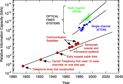
Figure 2. Local heating of central processing unit (CPU). This figure is from [Citation9], which is in black and white. Thanks to Y. Vlasov for the color version.[Citation10]
![Figure 2. Local heating of central processing unit (CPU). This figure is from [Citation9], which is in black and white. Thanks to Y. Vlasov for the color version.[Citation10]](/cms/asset/d9a7c5ab-8395-4fc5-b9f8-30b49be3fd2b/tsta_a_1301193_f0002_oc.gif)
The present paper reviews the conflict of on-chip DWDM and uncooled architectures, summarizes our survey on TO coefficients and bandgaps of various optical materials, and proposes a materials group of mid-index contrast optics (MiDex) materials for DWDM on a chip. The main results are as follows:
| (1) | Non-stoichiometric silicon nitrides (SiNx) are chosen as a typical MiDex material from the design figure and prepared by physical vapor deposition (PVD) and chemical vapor deposition (CVD) methods. | ||||
| (2) | These TO coefficients are precisely measured. The ring resonators are chosen as MUX/DEMUXs in the present work and prepared by PVD- and CVD-SiNx. These rings can lock the resonance frequency within 100 GHz in the temperature range | ||||
| (3) | The PVD-SiNx platform can be integrated in the CMOS back-end-of-line because there is no need for high temperature annealing to reduce N–H bond associated absorption at around 1520 nm. To fully meet the ITU-T protocol, the crosstalk of –30 dB, the channel spacing has to increase by 32 GHz in the present rings of Q of 31,600. Thus, the channel spacing must be 132 GHz, suggesting that further stabilization is required. | ||||
| (4) | Athermalization of the ring with a ‘silicone’ polymer shrinks the channel spacing to 50 GHz in the wavelength range from 1460 nm to 1620 nm (the so-called S, C, and L bands) for | ||||
| (5) | An extensive survey of MiDex materials, including materials with high dielectric constants (k), i.e. high k materials reported in Si-LSIs studies, is performed. It is proposed from the revised design figure that Al2O3, Ta2O5, Ga2O3, HfO2 and their alloys should be the choice of MiDex materials for on-chip DWDM implementation without athermalization. | ||||
MiDex-based electronic and photonic integrated circuits (EPICs) for DWDM are illustrated on a bulk Si wafer. In MiDex there is no need for a SOI wafer. The potential applications of the MiDex photonics are discussed, such as medical and environmental sensing, as well as data communication in vehicles and data centers.
2. Minimum channel spacing
The impact of temperature fluctuation on DWDM is explained in this section. Here, a ring resonator is used as MUX/DEMUX. Figure illustrates the relation between the filtering characteristics of the ring and the minimum channel spacing . It is assumed that the filtering wavelength is originally at
. The thermal shift amount of the wavelength
can be described by the EO coefficient of the ring material since
, where r denotes the ring radius, m integer multiple, and n(T) effective refractive index of the ring material. The linear-approximation can be
. Thus,
can be given by these equations. The wavelength
of the adjacent channel should fulfill
to prevent MUX/DEMUX from malfunctioning. In other words, the minimum channel spacing
Here,
is the crosstalk and given by:[Citation11]
(1)
(1)
(2)
(2)
Figure 3. Minimum channel spacing. Thermal shift and crosstalk should determine the minimum channel spacing.
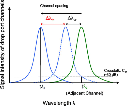
The filter spectrum is written by the Lorenz function and Q denotes the quality factor of the ring. Accordingly, to fulfill the ITU-T recommendation
Table shows the crosstalk as a function of Q at 1550 nm. The crosstalk recommended by ITU-T is –30 dB. Assuming no thermal shift, the minimum channel spacing should be
; 107 GHz when Q is 10,000, and 10.7 GHz when Q is 100,000. We have also added the case of –20 dB crosstalk in Table , as assumed in [Citation12]. The crosstalk of –20 dB seems beneficial in the minimum channel spacing, but the effect is not too large. This, together with the large TO coefficient of Si shown later, clearly indicates that the ITU-T recommendation is very difficult for Si photonics to meet. Therefore, it is important to find a material group of a small TO coefficient and with the ring of high Q for MUX/DEMUX. The goal of the present study is to find the material group of small TO coefficients for Si photonics to implement on-chip DWDM.
Table 1. The relation of minimum channel spacing with Q factor at 1550 NM.
3. MiDex Si photonics platform
Figure (a) shows the design of the minimum bending radius and scattering loss of waveguide vs. index difference () between waveguide core and cladding [Citation1]. Here, SiO2 is assumed as the cladding material. Si photonics has been catalyzed by its high
, allowing a small minimum-bending radius of the waveguides, e.g. 1 μm, and thus requiring only a small footprint in integrated photonics. The index regime has been referred to as high-index contract optics by Haus [Citation11]. Following him, we referred it as a HiDex platform. Although a high scattering loss associated with high
was disadvantageous, high precision fabrication technologies developed for the CMOS fabrication has solved this drawback. In contrast, low-index contrast optics (LoDex) platform based on SiO2 fiber technology is advantageous in the high transmission at the cost of large minimum bending radii of the waveguide (>cm). There is a regime between HiDex and LoDex,
, here referred to as MiDex (mid-index contrast optics). The advantage of the regime as the platform is shown in Figure (b) with their TO coefficients and bandgaps vs.
[Citation13–16]. It is clearly seen that crystal Si (c-Si) as well as amorphous Si (a-Si) has a larger TO coefficient than the MiDex materials, here LiNbO3, AlN, stoichiometric silicon nitride (Si3N4), and Al2O3. This strongly suggests that the MiDex platform should be more robust to thermal fluctuation than HiDex platforms.
Figure 4. Materials chart for Si photonics platform. MiDex and HiDex are shown. Horizontal axis shows the optical index difference, Δn = ncore – nclad at 1.55 μm, where the cladding is SiO2. (a) Design figure for minimum bending radius and scattering loss with experimental results shown by squares. (b) Design figure for thermo-optic coefficient and bandgap of materials group. Symbols show literature data. Calculation of minimum bending radius is regarding that bending loss less than 0.1 dB/turn as acceptable.
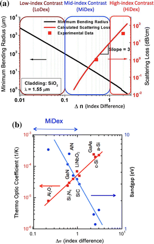
A small TO coefficient is a necessary condition for DWDM implementation in Si photonics. The sufficient condition is a large bandgap. Since implementing many wavelength channels in DWDM increases the overall optical power transmitting in the Si waveguide, light is absorbed through optical nonlinear phenomena in Si. The light energy of 1550 nm is 0.8 eV, and the bandgap of Si is 1.12 eV at room temperature. Thus, two photon absorption and four wave mixing happen in the Si waveguide with an increase in the channel number. To avoid these nonlinear phenomena, we should set the minimum bandgap of waveguide materials, here 3 eV, which is more than three times larger than the light energy. It is clearly shown from Figure (b) that the MiDex materials have all cleared the sufficient condition as well.
Among these MiDex materials frequently used in electronic and photonics, the present paper has chosen Si3N4 because it is commonly used in Si CMOS chips. Si3N4 has a TO coefficient of 2.4 × 10⁻⁵ 1/K which is ~1/10 that of Si, and a bandgap of ~5 eV, which is ~5 times larger than that of Si. It should thus be an excellent example to understand how MUX/DEMUX of the MiDex material behaves under thermal fluctuation. Figure (a) also shows that Si3N4 on SiO2, i.e. , allows ~4 μm as the minimum bending radius, which is larger than that of Si but still acceptable on a Si chip of 1 × 1 cm2. The scattering loss is ~1 dB cm–1, which can be further reduced by high precision fabrication.
The drawback is that CVD-Si3N4 has N–H (nitrogen and hydrogen) bonds that induce light absorption at 1520 nm, and removing the bonds needs high temperature annealing, e.g. at 1100 °C. This prevents the Si3N4 platform from being implemented in the CMOS back-end-of-line. We will demonstrate that the PVD method solves the drawback as in Section 5.
There have been a large number of reports on this material set, stoichiometric Si3N4 on SiO2 to apply the waveguides. One of the earliest papers of its waveguide application was published in 1977 by Stutius and Streifer [Citation16], a decade earlier than the Si photonics proposal [Citation17]. They demonstrated its excellent characteristics as a waveguide core material at a visible wavelength (0.633 μm). Since then various fabrication technologies have been employed to deposit silicon nitrides on SiO2 to fabricate waveguides and resonators. Typical reports are on CVD [Citation18–27] and on PVD [Citation28–31]. Even optical transceivers based on silicon nitrides have been reported recently [Citation12,32,33]. However, there only a few publications on measurements of the TO coefficients of silicon nitrides on SiO2 [Citation15,25]. In [Citation25], PVD-based non-stoichiometric silicon nitride (SiNx) films were deposited to fabricate a photonic crystal structure to measure the TO coefficient. The TO coefficient reported was 0.47 × 10⁻⁴ 1/K at 1510 nm, which is twice higher than that reported in [Citation15] where a ring resonator was used but the material is stoichiometric Si3N4 and the fabrication method is CVD. Since stoichiometric Si3N4 has large built-in stress preventing a thick structure like waveguides, a clear demand exists for measurement of the TO coefficients of less stressed (thick enough) non-stoichiometric SiNx fabricated by both CVD and PVD at low temperature.
4. Fabrications
We used radio frequency (RF) reactive sputtering to deposit PVD-SiNx films on SiO2 thermally grown on Si. Here, Ar plasma with a Si target and ambient N2 were used. The substrate was kept at room temperature and the chamber pressure was controlled to be 0.5 Pa during the deposition process. SiNx films were also prepared using electron cyclotron resonance plasma enhanced CVD (ECR-CVD), which allows low temperature deposition and less stressed SiNx. The condition was 200 °Con the SiO2 on Si, using SiH4 and N2. However, even ECR-CVD-SiNx (CVD-SiNx hereafter) was limited to ~650 nm in thickness before showing cracks on the surface. Although the PVD-SiNx films can be deposited beyond 800 nm in thickness, 650 nm thick PVD-SiNx was chosen to deposit to compare the film qualities of CVD-SiNx. The refractive indices (n) of the as-deposited PVD- and CVD-SiNx films were measured to be 1.96 and 1.98 at 1551 nm using spectroscopic ellipsometry; n values of the films were slightly smaller than that of stoichiometric Si3N4 reported as 2. To reduce N–H bond-related absorption, high temperature annealing was performed on the CVD-SiNx film at two temperatures 900 and 1150 °Cfor 3 h in N2 gas flow. It should be noted here that the PVD-SiNx film was not annealed in the present paper. Finally, single mode waveguides and ring resonators were fabricated on the PVD-SiNx and on two kinds of the CVD-SiNx films with and without the annealing. We used an inductive coupled plasma reactive ion etching (ICP-RIE) with CHF3 gas. One mask set was used to ensure identical device structures on these PVD- and CVD-SiNx films. Typical waveguide structures were 650 nm thick and 1 μm wide SiNx on 15 μm-thick SiO2 on Si for single-mode propagation. The waveguide was 5 mm long. The transmission loss was measured by the cutback method. The ring resonator was 60 μm in radius and the gap between the ring and the waveguide was 400 nm wide. The upper cladding was air. The resonance peaks of these rings were measured at temperatures from room temperature (24 °C) to 76 °Cto measure the TO coefficients of these PVD- and CVD-SiNx films. For temperature calibration of the heating unit, a Si ring resonator fully covered with SiO2 cladding was prepared, considering the mode confinement factor. Athermalization to further stabilize the wavelength channel was studied using a ‘silicone’ polymer as the upper cladding.
5. Results and analysis
5.1. Waveguides and ring resonators
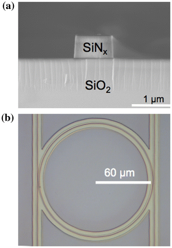
Figure shows scanning electron microscopy (SEM) images of typical waveguides and coupled ring resonators fabricated using the PVD method [Citation13]. The waveguides and ring resonators are fabricated as designed. No cracks were observed on PVD- and CVD-SiNx, indicating their small built-in stress in the present non-stoichiometric SiNx.
Figure 5. Typical SEM images of fabricated SiNx. (a) A cross sectional SEM image, (b) a plan view image of SiNx ring and coupled waveguides used in the present work.
5.2. N–H bond related absorption
Figure shows transmission characteristics of the PVD- and CVD-SiNx waveguides [Citation13]. It is clearly shown in Figure (a) that the PVD-SiNx waveguide (red) has no absorption peak, while the CVD-SiNx waveguide (black) without annealing has a broad absorption peak centered at 1520 nm. The peak still remains after the sample is annealed at 900 °Cfor 3 h (blue) but disappears by annealing at 1150 °Cfor 3 h and is similar to that of the PVD-SiNx. Therefore, it is fair to conclude that the absorption is generated by N–H bonds in the CVD-SiNx film, and that the absorption is not detected in the PVD-SiNx film. The PVD process does not use any hydrogen, and thus no absorption at 1520 nm is quite reasonable.
Figure 6. Transmission characteristics of PVD- and CVD- SiNx waveguides on SiO2. (a) Transmission spectra. The PVD-SiNx waveguide is shown in red, the CVD-SiNx is plotted in black and in blue (annealed at 900 °Cfor 3 h). The transmission loss of the CVD-SiNx after 1150 °Cannealing for 3 h (not shown here) is identical to that of the PVD-SiNx (red). (b) The transmission loss of the PVD-SiNx waveguide. The loss ~5.6 dB cm–1 is obtained using the waveguide with air upper cladding. Simulation indicates that the loss is reduced to ~1 dB cm–1 with the SiO2 upper cladding.
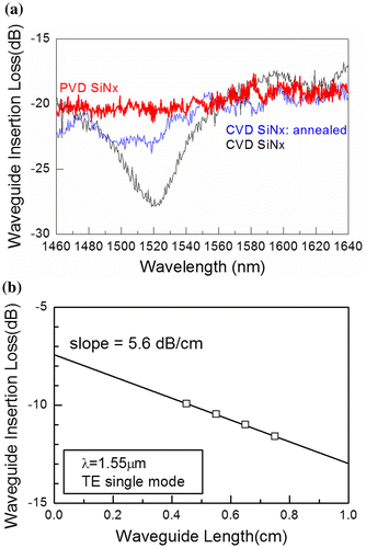
Figure (b) shows that the transmission loss of the PVD-SiNx waveguide is ~5.6 dB cm–1 at 1550 nm for the transverse electric (TE) mode. Finite difference time domain simulation indicated the transmission loss of the waveguide with air cladding would be associated with the sidewall scattering of the waveguide, and should reduce to ~1 dB cm–1 by a SiO2 upper cladding of the waveguide. This is the same as previously reported in CVD-SiNx [Citation21,22]. Therefore, the present PVD-SiNx waveguide is as transparent as the CVD-SiNx waveguide annealed at a high temperature.
The transmission loss in our waveguide is much lower than in previous reports on PVD-SiNx [Citation28–31]; tens of dB cm–1 even after 1050 °Cannealing for 2 h [Citation31]. There are at least two differences from the present study: (i) their n reported was ~2.2, while ours was 1.96; (ii) their PVD-SiNx was deposited using a SiNx target while ours used a Si target with nitrogen plasma. The difference in n strongly suggests that their PVD-SiNx would be Si-rich, which may result in the high transmission loss in terms of scattering. However, n of 2.2 was also reported in CVD-SiNx waveguides by other researchers [Citation19], showing the transmission loss was only 2.1 dB cm–1. The difference between [Citation31] and the present work still exists in the SiNx target. Assuming that the target was prepared by CVD and contains a high density of N–H bonds, the low transparency can be understood. However, their loss does not decrease even after 1050 °Cannealing for 2 h, which should be enough high to anneal hydrogen out. Thus, it is fair to say that the origin of the high transmission loss reported remains unclear.
To summarize the results we obtained here:
| (1) | The waveguides fabricated from as-deposited PVD-SiNx film are as transparent as the ones from CVD-SiNx annealed at a high temperature to remove N–H bonds. | ||||
| (2) | The transmission loss of the PVD-SiNx waveguide is ~5.6 dB cm–1 with an air-cladding. Simulations suggest it reduces to ~1 dB cm–1 with a SiO2 upper cladding, which is the same as the reported results on CVD-SiNx after the high temperature annealing. | ||||
In addition, PVD SiNx is advantageous over CVD-SiNx in the maximum thickness of deposited layers, due to its lower built-in stress. This is beneficial to minimize so called polarization depend loss.
5.3. Measurement of thermo-optic coefficient
In DWDM implementation it is required that the channel wavelength of MUX/DEMUX should be unchanged under thermal fluctuation. The thermal shift in resonance peaks of ring resonators can be expressed as:(3)
(3)
where λp is the resonance wavelength peak, and ng and neff are group index and effective index, respectively. Equation (3) does not take into account the effects of the wavelength dispersion of the TO coefficient, of the second order terms and of the thermal expansion coefficient. The right side of Equation (3) is obtained by solving the propagation mode shape in the present waveguides with the refractive index profile. The refractive indices and TO coefficients 1/K of Si, CVD-SiNx, and SiO2 at ~1550 nm were 18.0 × 10⁻⁵ [Citation34,35], 2.45 × 10⁻⁵ [Citation14], and 0.85 × 10⁻⁵ [Citation14].
Figure shows the measured peaks in transmission spectra with Lorentzian fittings [Citation13]. The quality factor Q of these peaks is calculated to be 31,600. Measured peak shifts are 20.4 and 16.2 pm K–1 for the PVD- (blue) and CVD-SiNx (red) rings. The CVD-SiNx result agrees extremely well with a previous report [Citation15], which indicates that the TO coefficient of CVD-SiNx is almost same as the reported stoichiometric Si3N4, but a half of that report [Citation25]. In [Citation25], photonic crystal structures of multilayer stacks were used to measure the TO coefficient, while the present study and the report [Citation13] use thin layer structure of ring resonators. It may be fair to say that the origin of the TO coefficient difference from [Citation25] would be the multilayer stack structure of their photonic crystal, most likely stress induced by the stack structures. On the other hand, the PVD-SiNx results show a slightly larger TO coefficient, i.e. 2.8 × 10⁻⁵ 1/K, than CVD-one. The origin of the difference is not clear.
Figure 7. Transmission characteristics of the PVD- and CVD-SiNx ring resonators at temperatures from room temperature (24 °C) to 76 °C. (a) The spectra of the drop port show Q of 31,600. (b) The resonance peak shifts of CVD-SiNx rings are reproduced by the reported thermo-optic coefficient, 2.4 × 10⁻⁵ 1/K, obtained for CVD stoichiometric Si3N4.[Citation15] The shifts are slightly larger for PVD than CVD rings. The thermo-optic coefficient of the PVD-SiNx is 2.8 × 10⁻⁵ 1/K.
![Figure 7. Transmission characteristics of the PVD- and CVD-SiNx ring resonators at temperatures from room temperature (24 °C) to 76 °C. (a) The spectra of the drop port show Q of 31,600. (b) The resonance peak shifts of CVD-SiNx rings are reproduced by the reported thermo-optic coefficient, 2.4 × 10⁻⁵ 1/K, obtained for CVD stoichiometric Si3N4.[Citation15] The shifts are slightly larger for PVD than CVD rings. The thermo-optic coefficient of the PVD-SiNx is 2.8 × 10⁻⁵ 1/K.](/cms/asset/8598fd1b-3831-46de-9966-88ecbcc03c0d/tsta_a_1301193_f0007_oc.gif)
In conclusion, the thermal shift of the peaks of PVD- and CVD-SiNx rings are within 100 GHz at = 52 °C, while that of the Si peak moves by 100 GHz at
<10 °C. Considering that the ITU-T recommendation of the crosstalk is –30 dB, the minimum channel spacing of the present SiNx ring should be 136 GHz according to Table . It is clear that our MiDex platform, non-stoichiometric SiNx core and SiO2 cladding, is suitable to implement DWDM on a chip with the minimum channel spacing of 136 GHz. However, further stabilization is required to achieve 100 GHz or narrower spacing.
5.4. Athermalization
Athermalization is known to be effective to stabilize the channel wavelength, using an uppercladding material with its negative index dependence on temperature [Citation36]. This is expressed as:
(4)
(4)
Here, Γ denotes the mode’s confinement factor of the mode, the subscript cr is the core, and cl is the cladding.
The thermal peak shifts of athermalized PVD-SiNx rings we measured are shown in Figure . Here, a polymer ‘silicone’ sold by Shin-Etsu Chemical Co (13-1, Isobe 2-chome, Annaka, Japan). Ltd is used for athermalization. We first used spectroscopic ellipsometry to measure the thermo-optic coefficient of silicone using the same heating setup we used:(5)
(5)
Figure 8. The peak wavelength shift of the PVD-SiNx ring resonators with athermalization using a ‘silicone’ polymer as the upper cladding (red). The shifts were measured between 24 and 70 °C. The black and red lines are simulations. An athermalized SiNx (MiDex) ring shows a smaller thermal shift than reported for an athermalized Si rings (black).[Citation36] The athermalized SiNx ring covers S-, L- and U-bands within the 50 GHz channel spacing at this temperature range, while the reported, athermalized Si rings cover C band.
![Figure 8. The peak wavelength shift of the PVD-SiNx ring resonators with athermalization using a ‘silicone’ polymer as the upper cladding (red). The shifts were measured between 24 and 70 °C. The black and red lines are simulations. An athermalized SiNx (MiDex) ring shows a smaller thermal shift than reported for an athermalized Si rings (black).[Citation36] The athermalized SiNx ring covers S-, L- and U-bands within the 50 GHz channel spacing at this temperature range, while the reported, athermalized Si rings cover C band.](/cms/asset/8d0ef1ba-9cdd-4a86-8c97-6191c599fc87/tsta_a_1301193_f0008_oc.gif)
The thermal peak shifts of the SiNx ring are measured at the same temperature range employed in [Citation36], i.e. room temperature and 70 °Cin a wider wavelength range from 1490 nm to 1630 nm. The shifts calculated using Equations (4) and (5) are shown in red, which reproduces the peak shifts of the SiNx ring quite well. It is demonstrated that the peak shifts of the athermalized SiNx ring is within 0.4 nm, i.e. 50 GHz in the S-, C-, and L-band in this temperature range. While preserving the crosstalk of -30 dB shown in Table , the minimum channel spacing should be 86 GHz <100 GHz, which meets ITU-T recommendation. On the other hand, the thermal peak shift of athermalized Si rings reported using TM mode [Citation36] is also plotted in Figure , indicating that there is no thermal shift at 1530 nm between room temperature and 70 °C. However, it is hard to keep the athermalization effect in a wider wavelength range as well as for TE modes since the mode profile in the Si waveguide is sensitive to its wavelength and waveguide cross section.
It is concluded that athermalization is an excellent way to further stabilize the MiDex channel wavelength against thermal fluctuation on a chip as well. Indeed, athermalized SiNx rings with the silicone polymer demonstrate its great potential to lock the channel wavelength in a wider wavelength range than athermalized Si rings. Further optimization including both TE and TM athermalization will help MUX/DEMUX implemented on a DWDM chip.
6. Discussion
6.1. Ultimate MiDex material candidates for DWDM
Further stabilization of the channel wavelength can be done by choosing the other MiDex materials. Figure shows more MiDex materials [Citation37–42] as also shown in Table . Among them, the following four materials: (1) Al2O3, (4) HfO2, (7) Ta2O5 and (12) Ga2O3 should be excellent candidates because of their low TO coefficient <10−5 1/K and the bandgap >4 eV. It is interesting to note that Ta2O5 has the smallest TO coefficient, 0.23 × 10⁻⁵ 1/K, which is even smaller than that of SiO2. Δn of Ta2O5 core and SiO2 cladding is 0.76, allowing 4 μm as the minimum bending radius as in Figure (a). Since the TO coefficient is one order of magnitude smaller than that of SiNx, simple extrapolation of the present SiNx results to Ta2O5 suggests that the thermal shift of the Ta2O5 ring resonance would be only a few pm K–1 at . In addition, Δn of Al2O3 is 0.32, which requires 100 μm of the minimum bending radius, while Ga2O3 has Δn of ~0.5, allowing ~4 μm of the minimum bending radius. Therefore, a strong demand exists to fabricate the waveguide structures of the ring of these materials and their alloys and to measure transmission losses as well as mechanical (stress) and thermal stability. In addition to these materials, silicon oxynitride (SiOxNy) is proposed to tune the index by choosing the alloy composition [Citation26]. It should also be noted that the TO coefficient of the alloy can be controlled in a range possibly between 0.24 × 10⁻⁴ of SiNx (the present work), and 0.85 × 10⁻⁵ of SiO2 [Citation14]. It is important to learn how much we can reduce the TO coefficient in this alloying, since the alloy has already been applied to the waveguides using CMOS technology.
Figure 9. Design figure of thermo optic coefficient (blue circles) and bandgap (red squares) vs. Δn. The PVD-SiNx and CVD-SiNx are within the green circle of Si3N4. The following four materials, (1) Al2O3, (4) HfO2, (7) Ta2O5 and (12) Ga2O3, should be excellent candidates because of their low TO coefficients < 10−5 1/K and the wide bandgaps >4 eV.
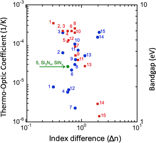
Table 2. The MiDex materials characteristics.
6.2. Monolithic EPICs on Si bulk wafers
The MiDex platform can be fabricated on any substrates including glass or polymer, in fact, any substrates. It should be noted that the recent demonstration of Ge laser diodes (LDs) on Si [Citation43–45] clearly indicates that the MiDex platform is an enabler of ‘monolithic’ EPICs with no hybrid bonding of lasers. There have already been quite a few reports on Si photonics on Si bulk wafers and even on a CMOS chip with a high density, high performance transistors [Citation46,47,49–53]. They were crystalline or amorphous Si waveguides fabricated on air cavities as under cladding, which were post-fabricated by etching after entire CMOS chip fabrication. Thermal fluctuation on a chip by its operation [Citation9,10] must be cancelled by local heaters to keep the temperature of the Si rings unchanged. The challenge is the power consumption. On the other hand, only a few papers on the MiDex platform on Si bulk wafer have been reported [Citation13,54–57]. In [Citation55], CVD-SiNx waveguides with rings were fabricated on a CMOS chip. The challenging issue is the reduction of the N–H bonds induced by the CVD process since a high temperature annealing is not applicable to CMOS circuitry under the waveguides. PVD-SiNx presented in this paper should be a viable solution for the issue.
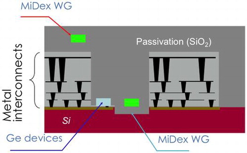
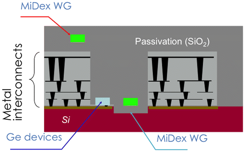
Figure illustrates a cross-sectional monolithic EPIC on a Si bulk platform. An application to a many-core chip is shown. With multilayer metal interconnection in the electronics part, Ge should be on Si next to electronics, and the MiDex waveguides can be on or between electronics parts as in the figure. There should be trenches on the Si wafer a couple of μm deep, which are filled with SiO2. Ge devices such as lasers, modulators, photodetectors, and MiDex waveguides could be located at the same height for a smooth coupling of the MiDex waveguide and the Ge devices and to avoid substrate coupling of the MiDex waveguides.
Figure 10. Schematics of a monolithic electronic and photonic integrated circuits on a Si bulk wafer (cross section). WG stands for waveguide.
6.3. Application of MiDex Si photonics
Recently, optical data communication in vehicles has attracted strong interests because of their lower weight and faster data transmission rate as compared to existing metal cables for electrical communications. Self-driving vehicles will transfer much more information than conventional cars. Also, the ambient temperature in vehicles is relatively high. Thus, since MiDex materials are robust to temperature fluctuations, there should be a strong need for MiDex Si photonics in the automotive industry. Furthermore, in-vehicle optical communications use visible light centered at around 550 nm (2.25 eV), because it fits best to the highest transmission window of plastic optical fiber (POF), and hence cannot employ Si waveguides. However, the MiDex materials are transparent in visible range because of their bandgaps (>3 eV). For example, a Si3N4 waveguide has been used at 633 nm [Citation16]. SiNx single-mode waveguides have also been grown by plasma-enhanced CVD for operation at 532, 780, and 900 nm with a loss below 0.5 dB cm–1 [Citation56]. Meanwhile, photodetectors for in-vehicle communication do not have to be transparent and can be Si, which is available as the substrate.
In addition to the in-vehicle communication, there are many potential applications such as sensing of gas molecules in medical and environmental fields [Citation57,58], besides existing application in e.g. data centers. Development of MiDex materials science, engineering, process and integration on Si is the key to success.
7. Conclusions
The mid-index contrast optics (MiDex) materials have smaller thermo-optic coefficients and wider bandgaps than Si and other high-index contrast optics (HiDex) materials do. Thus, the MiDex Si photonics platform should be robust to large thermal fluctuation on a chip and to high power transmission in terms of many wavelength channels. This opens up a new era employing the architecture of dense wavelength division multiplexing (DWDM) on a chip. To demonstrate the potentiality of the platform, we chose non-stoichiometric silicon nitride (SiNx) as a typical MiDex material, and physical vapor deposition (PVD) and chemical vapor deposition (CVD) methods for fabrication. It is demonstrated that the TO coefficients are 2.4 × 10⁻⁵ 1/K for the CVD-SiNx and 2.8 × 10⁻⁵ 1/K for the PVD-SiNx. The CVD- and PVD-SiNx rings have locked the peak within 100 GHz in the temperature range 24–76 °C, while they have locked within 136 GHz in the same temperature range when the crosstalk of –30 dB is considered. The athermalized SiNx ring with a silicone polymer as an upper cladding further stabilizes the thermal peak shift within 86 GHz in the S, C, and L-bands in the same temperature range without the crosstalk. This meets the ITU-T protocol for DWDM. PVD-SiNx needs no high temperature annealing to evacuate hydrogen, and thus is ready for the implementation in the CMOS back-end-of-line. The survey of MiDex materials indicates that Al2O3, HfO2, Ta2O5 and Ga2O3 should be excellent candidates for DWDM because of their low TO coefficient <10−5 1/K. All the MiDex platforms including these new materials have wide bandgaps >3 eV and thus should have negligibly small optical nonlinearity at 1.55 μm. This allows DWDM implementation on electronic and photonic integrated circuit (EPIC) chips. The platform also allows manufacturing monolithic EPICs on Si bulk wafers.
Si photonics has not been an attractive field for material scientists and engineers, since EPICs can be fabricated using only CMOS materials and process technologies, which are already established for current LSIs. However, recent demand due to a significant increase in information capacity for computation and communication requires on-chip DWDM. It is now important that materials scientists and engineers use their expertise to enable development of the MiDex platform on Si.
Disclosure statement
No potential conflict of interest was reported by the authors.
Funding
The research results were supported by ‘R&D on optical PLL device for receiving and monitoring optical signals’, the Commissioned Research of National Institute of Information and Communications Technology (NICT), JAPAN.
Acknowledgments
A series of equipment for fabrication in this work was provided by VDEC in Takeda Clean Room. We appreciate Prof. T. Kondo of University of Tokyo and Prof. K. Ohashi of Waseda University for their invaluable discussions.
References
- Kimerling LC, Kwong DL, Wada K. Scaling computation with silicon photonics. MRS Bull. 2014;39:687. 10.1557/mrs.2014.165
- Yamada K, Tsuchizawa T, Nishi H, et al. High-performance silicon photonics technology for telecommunications applications. Sci Technol Adv Mater. 2014;15:024603. 10.1088/1468-6996/15/2/024603
- Chaisakul P, Marris-Morini D, Rouifed MS, et al. Recent progress in GeSi electro-absorption modulators. Sci Technol Adv Mater. 2014;15:014601. 10.1088/1468-6996/15/1/014601
- Shoji Y, Mizumoto T. Magneto-optical non-reciprocal devices in silicon photonics. Sci Technol Adv Mater. 2014;15:014602. 10.1088/1468-6996/15/1/014602
- Ye H, Yu J. Germanium epitaxy on silicon. Sci Technol Adv Mater. 2014;15:024601. 10.1088/1468-6996/15/2/024601
- Baba T, Nguyen HC, Yazawa N, et al. Slow-light Mach-Zehnder modulators based on Si photonic crystals. Sci Technol Adv Mater. 2014;15:024602. 10.1088/1468-6996/15/2/024602
- Wada K, Kimerling L-C. Photonics and electronics with germanium. Weinheim: Wiley, 2015.
- Kimerling, LC. Photons to the rescue: microelectronics becomes microphotonics. ECS Interface. 2000;9(2): 15–20.
- Hamann HF, Weger A, Lacey JA, et al. “Hotspot-Limited Microprocessors: direct temperature and power distribution measurements”. IEEE J. Solid-State Circuits. 2007;42(1):56–65. 10.1109/JSSC.2006.885064
- Vlasov Y. private communication.
- Manolatou C, Haus HA. Passive components for dense optical integration. New York: Springer Science-Business Media, LLC; 2002. p. 1. 10.1007/978-1-4615-0855-7
- Doerr CR, Chen L, Buhl LL, et al. Eight-Channel SiO2 /Si3N4/Si/Ge CWDM receiver. IEEE Photonics Technol Lett. 2011;23(17):1201–1203. 10.1109/LPT.2011.2158091
- Zhang, Z, Yako, M, Ju K, et al. A silicon nitride platform by physical vapor deposition for dense wavelength division multiplexing on chip. IEEE Group Four Photonics. 2014, ThP25.
- Gosh G. Handbook of thermo-optic coefficients of optical materials with applications. San Diego: Academic Press; 1998.
- Arbabi A, Goddard LL. Measurements of the refractive indices and thermo-optic coefficients of Si3N4 and SiO(x) using micro ring resonances. Opt. Lett. 2013;38:3878–3881. 10.1364/OL.38.003878
- Stutius W, Streifer W. Silicon nitride films on silicon for optical waveguides. Appl Optics. 1977;16(12):3218–3222. 10.1364/AO.16.003218
- Soref, RA, Larenzo, JP. All-silicon active and passive guided-wave components for 1.3 and 1.6 μm, IEEE J Quant Electron. 1986;22(6):873–879.
- Dai D, Wang Z, Bauters JF, et al. Low-loss Si3N4 arrayed-waveguide grating (de)multiplexer using nano-core optical waveguides”. Opt. Express. 2011;19(15):14130. 10.1364/OE.19.014130
- Barwicz T, Popovic MA, Rakich PT, et al. Microring-resonator-based add-drop filters in SiN: fabrication and analysis. Opt. Express. 2004;12(7):1437–1442. 10.1364/OPEX.12.001437
- Kimerling LC, Negro L, Saini, S, et al. Monolithic silicon microphotonics”. Appl Phys. 2004;94:89–121. 10.1007/b11504
- Melchiorri M, Daldosso N, Sbrana F, et al. Propagation losses of silicon nitride waveguides in the near-infrared range. Appl Phys Lett. 2005;86:121111. 10.1063/1.1889242
- Sherwood-Droz N, Gondarenko A, Lipson M. Scalable 3D dense integration of photonics on bulk silicon. Opt Express. 2011;19:17761.
- Li Q, Eftekhar AA, Sodagar M, et al. Vertical integration of high-Q silicon nitride microresonators into silicon-on-insulator platform. Opt Express. 2013;21(15):18236. 10.1364/OE.21.018236
- Romero-García S, Merget F, Zhong F, et al. Silicon nitride CMOS-compatible platform for integrated photonics applications at visible wavelengths. Opt Express. 2013;21(12):14036. 10.1364/OE.21.014036
- Zanatta AR, Gallo IB. The thermo optic coefficient of amorphous SiN films in the near-infrared and visible regions and its experimental determination. Appl. Phys. Express. 2013;6:042402. 10.7567/APEX.6.042402
- Okazaki, K, N, Hidetaka, Tsuchizawa, T, et al, Optical coupling between SiOxNy waveguide and Ge mesa structures for bulk-Si photonics platform. IEEE Group Four Photonics. 2015;WP43:122
- Doris KTQian Wang, N, Wang, T, et al. Exploring high refractive index silicon-rich nitride films by low-temperature inductively coupled plasma chemical vapor deposition and applications for integrated waveguides”. ACS Appl Mater Interfaces. 2015;7:21884.
- Sparacin, D. Process and design techniques for low loss integrated silicon photonics Ph. D thesis. Massachusetts Institute of Technology; 2000.
- del Giudice M, Bruno F, Cicinelli T, et al. Structural and optical properties of silicon oxynitride on silicon planar waveguides. Appl. Optics. 1990;29(24):3489. 10.1364/AO.29.003489
- Kim JH, Chung KW. Microstructure and properties of silicon nitride thin films deposited by reactive bias magnetron sputtering. J Appl Phys. 1998;83:5831. 10.1063/1.367440
- Sandland, J Sputtered silicon oxynitride for microphotonics: materials study Ph. D thesis. Massachusetts Institute of Technology; 2005.
- Chen L, Doerr CR, Buhl L, et al. Monolithically integrated 40-wavelength demultiplexer and photodetector array on silicon. IEEE Photonics Technol. Lett. 2011;23(13):869–871. 10.1109/LPT.2011.2141128
- Martens D, Subramanian AZ, Pathak S, et al. Compact silicon nitride arrayed waveguide gratings for very near-infrared wavelengths. IEEE Photonics Technol Lett. 2015;137:2702.
- Gai X, Yu Y, Kuyken B, et al. Nonlinear absorption and refraction in crystalline silicon in the mid-infrared Laser. Photon Rev. 2013;7:1054. 10.1002/lpor.201300103
- Komma J, Schwarz C, Hofmann G, et al. Thermo-optic coefficient of silicon at 1550 nm and cryogenic temperatures. Appl Phys Lett. 2012;104:1905.
- Raghunathan V, Ye WN, Hu H, et al. Athermal operation of Silicon waveguides: spectral, second order and footprint dependencies. Opt Express. 2010;18:17631. 10.1364/OE.18.017631
- Bhaumik, R. Bhatt, S. Ganesamoorthy, A, et al. Temperature- dependent index of refraction of monoclinic Ga2O3 single crystal. Appl. Optics. 2011;50(31):6006. 10.1364/AO.50.006006
- Robertson J. Band offsets of wide-band-gap oxides and implications for future electronic devices. J Vac Sci Technol. 2000;18(3):1785.10.1116/1.591472
- Elalamy Z, Drouard E, Govern T, et al. GThermo-optical coefficients of sol–gel ZrO2 thin films. Opt. Communications. 2004;235:365–372. 10.1016/j.optcom.2004.02.043
- Tanner C, Geisinger K, Wusirika R. Temperature and wavelength dependence of refractive index of zircon and hafnon. Opt Mater. 2004;26:305–311. 10.1016/j.optmat.2003.12.008
- Chu AK, Lin HC, Cheng WH. Temperature dependence of refractive index of Ta2O5 Dielectric Films. J Electron Mater. 1997;26(8):889–892. 10.1007/s11664-997-0269-3
- Charles H. Lange, D Duncan, D, Temperature coefficient of refractive index for candidate optical windows. Proc. SPIE 1326, Window and Dome Technologies and Materials II. 1990;71:12–15. 10.1117/12.22483.
- Liu J, Sun X, Camacho-Aguilera R, et al. Ge-on-Si laser operating at room temperature. Opt. Lett. 2010;35(5):679–681. 10.1364/OL.35.000679
- Camacho-Aguilera RE, Cai Y, Patel N, et al. An electrically pumped germanium laser”. Opt. Express. 2012;20(10):11316. 10.1364/OE.20.011316
- Koerner R, Oehme M, Gollhofer M, et al. Electrically pumped lasing from Ge Fabry-Perot resonators on Si. Opt. Express. 2015;23(11):14815. 10.1364/OE.23.014815
- Holzwarth CW, Orcutt JS, Li H, et al. OSA Conference on Laser and ElectroOptics/Quantum electronics and laser science, Paper# CThKK5, 2008.
- Batten C, Joshi A, Orcutt J, et al. Building manycore processor-to-DRAM networks with monolithic silicon photonics. 16th IEEE Symposium on High Performance Interconnects; 2008. p. 21.
- Orcutt JS, Khilo A, Holzwarth CW, et al. “Nanophotonic integration in state-of-the-art CMOS foundries. Opt. Express. 2011;19:2335.
- Lee BS, Cho KS, Shin YH, et al. Integration of photonic circuits with electronics on bulk-Si platform. IEEE Group Four Photonics. 2013;WA1.
- Hung S-C, Lin S-J, Chao J-J, et al. Fabrication of crystalline Si waveguides on (1 0 0) bulk Si substrate using laser reformation method. J. Lightwave Technol. 2013;31:3368. 10.1109/JLT.2013.2283216
- Sun C, Georgas M, Orcutt J, et al. A monolithically-integrated chip-to-chip optical link in bulk CMOS. IEEE J Sol-Stat Circuits. 2015;50(4):828–844. 10.1109/JSSC.2014.2382101
- Kim G, Park H, Joo J, et al. Single-chip photonic transceiver based on bulk-silicon, as a chip level photonic I/O platform for optical interconnects. Sci Rep. 2015;5:11329. 10.1038/srep11329
- Sun C, Wade MT, Lee Y, et al. Single-chip microprocessor that communicates directly using light. Nature. 2015;528(24):534–538.
- Luke K, Dutt A, Poitras CB, et al. Overcoming Si3N4 film stress limitations for high quality factor ring resonators. Opt Express. 2013;21(19):22829. 10.1364/OE.21.022829
- Zan Zhang Z, Beiju Huang X, Xu Zhang ZZ, et al. Monolithic integration of Si3N4 microring filters with bulk CMOS IC through post-backend process. IEEE Photonics Technol Lett. 2015;27(14):1543. 10.1109/LPT.2015.2429677
- Subramanian AZ, Neutens P, Dhakal A, et al. Low-Loss singlemode PECVD silicon nitride photonic wire waveguides for 532–900 nm wavelength window fabricated within a CMOS pilot line. IEEE Photon. J. 2013;5(6):2202809. 10.1109/JPHOT.2013.2292698
- Lin PT, Singh V, Lin H-Y, et al. Low-Stress silicon nitride platform for Mid-Infrared broadband and monolithically integrated microphotonics, Adv. Opt. Mater. 2013;1(10):732–739. 10.1002/adom.v1.10
- Singh V, Lin P-T, Patel N, et al. Mid-infrared materials and devices on a Si platform for optical sensing. Sci Technol Adv Mater. 2014;15(1):014603. 10.1088/1468-6996/15/1/014603