
 ?Mathematical formulae have been encoded as MathML and are displayed in this HTML version using MathJax in order to improve their display. Uncheck the box to turn MathJax off. This feature requires Javascript. Click on a formula to zoom.
Abstract
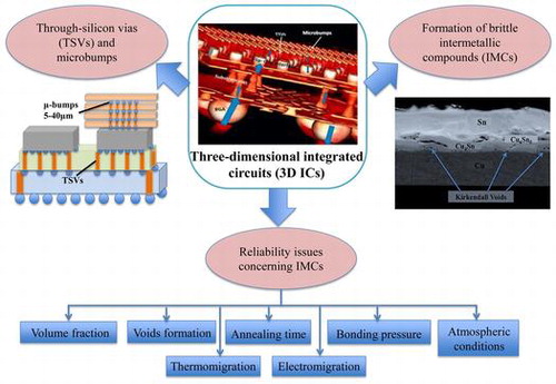
The high performance and downsizing technology of three-dimensional integrated circuits (3D-ICs) for mobile consumer electronic products have gained much attention in the microelectronics industry. This has been driven by the utilization of chip stacking by through-Si-via and solder microbumps. Pb-free solder microbumps are intended to replace conventional Pb-containing solder joints due to the rising awareness of environmental preservation. The use of low-volume solder microbumps has led to crucial constraints that cause several reliability issues, including excessive intermetallic compounds (IMCs) formation and solder microbump embrittlement due to IMCs growth. This article reviews technologies related to 3D-ICs, IMCs formation mechanisms and reliability issues concerning IMCs with Pb-free solder microbumps. Finally, future outlook on the potential growth of research in this area is discussed.
Introduction
In the past several decades, the semiconductor industry has seen the integration of many electronic components such as resistors, transistors and capacitors onto silicon chips, creating so-called two-dimensional integrated circuits (2D ICs). The exponential growth in the number of transistors per unit area or density of circuits per chip has been in line with Moore’s law prediction. However, Moore’s law is momentarily near the end of its prediction due to physical limitations as well as economic constraints. To overcome these problems, the microelectronics industry is attempting to combine chip and packaging technologies by stacking chips vertically. Vertical stacking was introduced in the late 1990s by Matsumoto et al. [Citation1]. They demonstrated a permanent wafer bonding technology with polycrystalline through-silicon via (TSV), namely the via-first approach for 3D ICs. This was followed by Ramm et al. [Citation2], who proposed a temporary wafer bonding technology with W-TSVs that combines the via-middle and via-last methodologies.
The accessible manufacturing approaches of 3D ICs by different design methods may have led to the integration of more electronic functionalities at shorter interconnect lengths [Citation3–5]. At the recent manufacturing level, 3D ICs consist of several layers of interconnected chips that are built on top of the Si chips. This is achieved by utilizing low joint volumes and thicknesses in the form of microbumps [Citation6–8]. This type of joint technology has rapidly grown in demand with great engineering efforts for vertical interconnects in conjunction with through-silicon via (TSV) [Citation9–13]. Thousands of microbumps solder joints are normally supported with two other types of joints, namely ball grid array (BGA) and flip-chip C-4 (or controlled collapse chip connection) solder joints to constitute the 3D ICs [Citation14].
The shift to lead (Pb)-free solder in solder microbumps is mainly intended to replace Pb-based solder that causes huge environmental and toxicity concerns [Citation15,16]. The selection of Pb-free solder is most often configured by Sn-based alloys such as Sn-Ag-Cu (SAC), Sn-Cu and Sn-Zn, which reveal good solder wettability and ultimately form a rod-type structure [Citation17,18]. However, in solder microbumps, the high diffusivity and quick reaction of Pb-free solder together with the shrinking chip dimensions offered by 3D ICs cause extensive formation of intermetallic compounds (IMCs) in the solder microbumps [Citation19,20]. Eventually, the excess IMCs appear brittle, particularly under drop conditions [Citation21]. Several studies have presented a clear failure mode change from ductile in the bulk solder to brittle in the IMCs layer when the parameters of aging time, deformation speed and IMCs layer thickness are increased [Citation22–24]. Lee et al. [Citation25] stated that the mechanical properties of a solder joint are dominated by the properties of the IMCs phase. Therefore, this paper presents a review of recent technologies comprising 3D ICs, namely TSV and microbumps, followed by IMCs mechanism formation and, lastly, reliability issues of microbumps concerning IMCs.
Three-dimensional integrated circuits: the technology
Monolithic three-dimensional integration (M3DI) technology is a scheme that enables 2D ICs to have multiple stacking device structures connected at the transistor level by robust electronic design automation (EDA) tools [Citation26,27]. Figure shows a schematic comparison of die-level or wafer-level three-dimensional interconnections that are distinguishable from one another.
Figure 1. Schematic comparison of three-dimensional (3D) interconnections of (a) stacked die package by wire bonding; (b) package on package by ball grid array (BGA); and (c) wafer and/or dies interconnected with through-silicon via (TSV) [Citation28].
![Figure 1. Schematic comparison of three-dimensional (3D) interconnections of (a) stacked die package by wire bonding; (b) package on package by ball grid array (BGA); and (c) wafer and/or dies interconnected with through-silicon via (TSV) [Citation28].](/cms/asset/13af49c3-cf18-4158-bb01-cf635c4ae649/tsta_a_1364975_f0001_oc.gif)
Compared with off-chip signalling 3D packaging, 3D ICs interact through on-chip signalling [Citation28,29]. In 3D ICs, the most significant elements of the enabling technology for handling and double-sided processing of extremely thin chips are the temporary bonding and debonding processes at lower temperature and higher throughput [Citation30]. A well-known bonding method that has become noteworthy in the production process for 3D ICs stacking minimization is thermal compression bonding, whereby two metals are ideally bonded together by heating and compression [Citation31,32]. The temperature for bonding requires that material diffusivity between two metal substrates and the solder be taken into account [Citation33]. Wu and Kumar [Citation34] mentioned that the capability of lower temperature bonding is important for relaxing the thermal stress induced by the coefficient of thermal expansion mismatch between the copper solder and silicon wafer. In low-temperature bonding, a sufficient amount of bonding materials in conjunction with suitable surface modifications between the upper and lower dies may assist the reaction phase formation and progression. For instance, to achieve transient liquid phase (TLP) bonding at less than 300 °C, utilizing molten gallium solder-platinum under bump metallurgy (UBM) triggers a liquid-solid reaction in the microbumps’ metallurgical structure bonding. Meanwhile, modifying the argon plasma-treated metal surface can lead to even lower temperature bonding (e.g. 200 °C) due to the solid state bonding reaction resulting from low surface roughness and a defect-free interface [Citation35–37].
Through-silicon via (TSV)
In 3D ICs technology, the TSV interconnection in chip stacking is introduced to provide connectivity between different designed parts for proper signal propagation and delivery, especially in high bandwidth and high-density dynamic random access memory (DRAM) [Citation38–42]. Sukharev [Citation43] and Lau [Citation44] reported finite element analysis simulations of TSV upon electromigration (EM) failure, which is when the TSV is unable to deliver the necessary voltage to any circuitry gate. Ryu et al. [Citation45] and Stiebing et al. [Citation46] suggested considering thermal cycling, which causes the TSV to extrude from the surrounding matrix or substrate. This phenomenon occurs due to a coefficient of thermal expansion mismatch between the surrounding substrate and the metal filler in TSV. Roh et al. [Citation47] overcame these reliability issues by alloying copper (Cu) together with tungsten (W) metal filler. It was observed that Cu-W alloy fills the TSV-Si substrate and exhibits no appreciable delamination compared to a single Cu-filled TSV-Si substrate.
Microbumps
A common 3-level solder joint packaging structure in 3D ICs is revealed in the three-dimensional view in Figure . The 3-level joint is positioned with a ball grid array (BGA) in the bottom row, controlled collapse chip connection (C4) flip-chip solder joints in the middle, and microbumps at the top between two silicon chips [Citation48]. The main purpose of solder joints in microelectronic devices is to provide good metallic bonding [Citation49,50].
Figure 2. Synchrotron radiation tomography of 3D ICs test sample with the blue arrows representing the electrical flow during device operation [Citation48].
![Figure 2. Synchrotron radiation tomography of 3D ICs test sample with the blue arrows representing the electrical flow during device operation [Citation48].](/cms/asset/c130ab45-250e-4217-bcec-c2f06f0abf46/tsta_a_1364975_f0002_oc.gif)
Microbumps are desirable for joining owing to their capability to increase the circuit density from the substrate sides to several miniaturization chips. The most well-known method of preparing microbumps is the soldering process [Citation51]. In this process, microbumps can be obtained in sizes ranging from 10 μm to 30 μm [Citation52–54]. In order to continuously scale down the microbumps size to 1 μm, the electroplating method is employed, which is subsequently followed by patterning the pillar-type structure of the microbumps [Citation55]. Talebanpour et al. [Citation11] suggested sandwiching electroplated microbumps between micron-size dies, while substrates are aimed to increase the aspect ratio of the solder joint. The intention is to mainly replace higher volume solder joints such as the flip-chip and lessen the requirement for expensive substrate design features [Citation25,56,57]. The post-prepared microbumps will undergo a reflow process at temperatures above the melting point of the solder and below the melting point of UBM or metal substrate. This process generally gives the solder microbumps a round shape, resulting in high-yield joining and superior electrical properties compared with non-reflowed microbumps [Citation50,58,59].
Since the size of microbumps has been progressively scaled down, the remaining challenge is mainly in the ability of the microbumps to preserve their mechanical stability whilst maintaining their function. The requirement to utilize underfill is approached for mechanical stability, and to enhance joint strength between stacked chips and prevent microbump corrosion [Citation60]. There are several methods of injecting underfill in the ultra-narrow gaps between the stacked chips. Fukushima et al. [Citation4] introduced microbump bonding through nonconductive film (NCF) to allow complete, void-less adhesive filler into the extremely narrow gaps between the chips and wafer by capillary force. The difficulty with underfill flowing by capillary force is the potential need for high external thermal compression to flatten the thin dies, which would then lead to additional mechanical reliabilities [Citation61]. Recently, Ohyama et al. [Citation62] mentioned that pre-applied fully coated underfill before bump bonding was already established in the 1990s, whereby no-flow of underfill was intended to attain both underfill and bump interconnection. However, underfill entrapment caused by both capillary force and pre-applied underfill may influence microbumps reliability. Liu et al. [Citation63] emphasized that there must not be any filler trapped in the extrusion of the compressed microbumps, otherwise they will exhibit poor electrical conduction. Ohyama et al. [Citation62] overcame these challenges by employing a hybrid bonding process, whereby the excess pre-applied underfill-coated microbumps are removed by polishing. The consequent several nanometres of the upper and lower half of the microbump tip can thus be perfectly bonded with no underfill entrapment.
IMCs formation
As extensions from the microbumps structure, the inevitable growth of intermetallic compounds (IMCs) between the solder and substrate can hugely influence the reliability of smaller solder sizes in 3D ICs [Citation64–66]. It is noted that the most popular metallurgy configurations of Pb-free solder microbumps are from copper (Cu) and tin (Sn)-based alloy with more than 97wt% Sn metal. The interdiffusion of this binary alloy is interestingly favoured due to the anisotropic properties offered by the tetragonal β-Sn phase [Citation67]. In general, the diffusion of metal atoms into the metallic semiconducting phase of β-Sn may differentiate the diffusion energy of the metal to be penetrated with respect to different crystallographic orientations governed by the β-Sn crystal structure [Citation68,69]. In terms of adsorption energy (Ead) and penetration energy (Epe), Table reveals that various M atoms are strongly adsorbed onto the surface and subsequently penetrate faster into the c-axis than the a-axis of Sn [Citation69].
Table 1. Different adsorption and penetration energies of M atoms on the a-axis and c-axis of Sn solder [Citation69].
In conjunction with this metallurgy, the IMCs formation of Cu and Sn binary systems has been increasingly and widely discussed [Citation70–72]. In order to successfully assemble a Cu and Sn binary system, a phase diagram and temperature profile of this binary alloy are necessary to understand the phase evolution resulting from their interactions (Figure ) [Citation73].
Figure 3. (a) Phase diagram [Citation74] and (b) bonding profile of binary Cu-Sn couple [Citation75].
![Figure 3. (a) Phase diagram [Citation74] and (b) bonding profile of binary Cu-Sn couple [Citation75].](/cms/asset/3d7c1aec-176e-4e71-b80a-b9d68949056b/tsta_a_1364975_f0003_oc.gif)
In the Cu-Sn system, two types of IMCs layers are normally present, namely η-Cu6Sn5 or Cu6Sn5 and ε-Cu3Sn or Cu3Sn. A number of intricate studies have been conducted to understand the microstructure of these IMCs [Citation76,77]. The IMCs configuration of soldered microbumps usually involves heating, reflow and solidification [Citation78,79]. During the early formation of Cu6Sn5 IMCs a liquid-state reaction takes place, whereby the molten Sn from the solder reacts directly with the Cu substrate, as per Equation (Equation1(1)
(1) ).
(1)
(1)
This is followed by a reflow process that facilitates a reaction between some remaining Sn atoms from soldering and the Cu6Sn5 interface formed earlier [Citation79]. As the process continues to progress, the subsequent solid-state reaction of Cu6Sn5 IMCs requires the diffusion of Cu atoms within Cu6Sn5 grains from small to large grains due to the distinct concentration gradient and different radii of Cu atoms. This phenomenon is known as Ostwald ripening [Citation80]. The Cu diffuses from smaller to larger grains, thus concurrently increasing the large Cu6Sn5 grains and shrinking the small grains. The diffusion coefficient, D, is expressed as the Arrhenius Equation (Equation2(2)
(2) ):
(2)
(2)
where is a pre-factor, Q is the activation energy for diffusion, T is the temperature and R is the gas constant (8.314 J/K mol). The growth of Cu6Sn5 is enhanced during solidification, because the super-saturated Cu atoms in the molten solder are rejected and precipitated on the existing Cu6Sn5 [Citation81]. The morphological transition of IMCs can be observed clearly in the solidification pattern, either in the eutectic or peritectic transformation, which denotes a stable solid-solid and solid-liquid equilibrium reaction [Citation82].
Likewise, thermal solid state aging causes a transformation from existing low-temperature Cu6Sn5 IMCs to existing high-temperature Cu3Sn IMCs [Citation11]. Ko et al. [Citation83] indicated that Cu3Sn arises largely from the consumption of Cu6Sn5, as in Equation (Equation3(3)
(3) ):
(3)
(3)
As the temperature increases, the extra energy gained by the Cu atoms at the substrate interface causes them to continue to react with pre-existing Cu6Sn5 until it grows into a thick layer and becomes a diffusion barrier to the Cu diffusion [Citation84]. This blocks the diffusion channel to the Cu6Sn5 layer and a Cu3Sn layer grows beneath it simultaneously [Citation85]. Therefore, the Cu3Sn layer is sustained between the Cu substrate and Cu6Sn5 IMC layer. The addition of a Ni layer in the Cu-Sn system may act as a diffusion barrier where no further Cu3Sn formation can occur [Citation86]. Temperature influences both the morphological shape and structure of the IMCs established at the same time. At low temperature (50 °C), the scallop-type Cu6Sn5 layer transforms into planar-like Cu6Sn5 until the temperature increases up to 150 °C, when it eventually grows into a uniform Cu3Sn layer [Citation87]. In the case of Ni-Sn solder, the large and round grains of Ni3Sn4 IMCs fully transform into whisker-type, coarsened grains when the annealing temperature is increased from 235 °C to 290 °C [Citation88].
Reliability issues concerning IMCs
Volume fraction
The brittle failure of IMCs, which are susceptible to concentrated stress, may cause structural defects in the microbumps [Citation89]. Therefore, it is vital to surpass the mechanical strength of the IMCs. The fracture toughness of a microbumps’ joint as a function of the volume fraction of IMCs was investigated by Talebanpour and Dutta [Citation90]. They have stated that the fracture toughness, GC, of the microbumps decreases with increasing IMC volume fraction, hIMC tot/hjt (total percentage of IMCs/strain rate). The hard constituents of IMCs replace the soft phase in the microbumps, and therefore, the increased IMC content enhances the apparent flow stress of the thinner solder joint. Joints with lower solder percentage can fracture much more easily than joints with greater solder content. This means that less plastic work dissipates in joints with lower solder content.
Void formation
The presence of voids in IMC structures is unavoidable as a result of atom migration upon reaching different thermal states. In IMCs established at low temperature, microvoids usually appear in the middle of the solder joint, due to molar volume changes resulting from the growth of Cu6Sn5 IMCs in the Sn solder [Citation91]. Meanwhile, in IMCs established at high temperature, numerous Kirkendall voids are produced due to the high-energy metal within the IMCs that triggers flow, leaving empty lattices behind. Minho et al. [Citation76] demonstrated Kirkendall voids in the Cu3Sn layer during annealing at high temperature of ~200 °C for 1 h (Figure (a)). In an electromigration test, the Kirkendall voids in Figure (b) may evoke current crowding, thus accelerating void propagation during current stressing [Citation92]. Consequently, the presence of voids enclosed in the IMCs will seriously affect the reliability of the microbumps [Citation93,94].
Figure 4. Scanning electron microscopy (SEM) images of Cu/Sn diffusion coupled with Kirkendall void formation at the Cu3Sn layer (a) without electromigration effect [Citation76] and (b) with electromigration effect [Citation95].
![Figure 4. Scanning electron microscopy (SEM) images of Cu/Sn diffusion coupled with Kirkendall void formation at the Cu3Sn layer (a) without electromigration effect [Citation76] and (b) with electromigration effect [Citation95].](/cms/asset/ae2fc1c8-86d6-48d5-baef-3867a21e55d1/tsta_a_1364975_f0004_oc.gif)
Annealing time
The behaviour and thickness of IMCs structure varies with increasing annealing time. It appears that both Cu6Sn5 and Cu3Sn IMCs follow a certain crystallographic orientation. As shown in the electron backscatter diffraction (EBSD) orientation maps in Figure , no preferred crystallographic orientation is found in the pre-existing Cu6Sn5 layer in the as-soldered state. After 24 h of annealing, the Cu6Sn5 layer has a dominantly favoured (0001) orientation [Citation96] and by further increasing the annealing time to 72 h, a Cu3Sn layer forms, which follows a (100) orientation.
Figure 5. EBSD orientation maps (TD) of Cu-Sn IMCs (RD: reverse direction and TD: transverse direction) [Citation96].
![Figure 5. EBSD orientation maps (TD) of Cu-Sn IMCs (RD: reverse direction and TD: transverse direction) [Citation96].](/cms/asset/5aa551fe-9c99-43d0-bddd-0c5daa865b01/tsta_a_1364975_f0005_oc.gif)
The total thickness of both Cu6Sn5 and Cu3Sn IMCs increases with increasing annealing time while other parameters are kept constant (Table ) [Citation97,98]. This is in agreement with the empirical power law relationship in Equation (Equation4(4)
(4) ) [Citation99].
(4)
(4)
Table 2. Analysis of total IMC thickness with respect to different aging times, constant atmospheric condition and constant temperature for each solder joint.
where indicates the IMCs layer thickness depending on time t; A is a growth constant; n is the time exponent; Q is the activation energy; R is the gas constant (8.314 J/K mol); T is the absolute temperature and k is the growth rate constant. This relationship can execute the mechanisms involved in IMCs growth, as determined by the time exponent, n. If n is 1, it indicates that IMCs growth is governed by the reaction rate. If n is 2, IMCs growth is influenced by the diffusion of reaction elements present, and if n is close to 3, growth is affected by a diffusion-controlled mechanism with coarsened IMC grains [Citation103].
Bonding pressure
Several research works have been carried out on applying distinct pressure in microbumps bonding. The different pressures applied promote varying microstructure growth and IMCs joint status while keeping other parameters, such as time and temperature, constant. At low soldering pressure, some areas of the microbumps may be disconnected and in loose contact with the desired position. This condition may cause smaller amounts of flowing metal solder during bonding, thus exhibiting a different microstructure evolution than under high soldering pressure on the final IMCs microstructure [Citation104]. The fracture behaviour of microbumps as a function of IMCs varies with the different bonding forces applied. The location of the shear stress applied changes from the Cu6Sn5 IMCs/solder bump interface to the UBM/Cu pillar bump interface, which implies that the fracture modes change as the bonding force increases [Citation105]. The fracture in the solder bump matrix is first ductile and then it transforms into a brittle mode upon reaching the IMCs area [Citation11]. The fracture modes fall into three categories: (1) fractures within the solder bump matrix, (2) interfacial fractures at the Cu6Sn5 IMCs/solder bump interface, and (3) interfacial fractures at the UBM/Cu pillar bump interface [Citation105]. Debonding or fracturing occurs at the lowest bonding point of the Cu6Sn5 IMCs/solder bump.
Atmospheric conditions
Exposing microbumps to different atmospheric conditions will eventually affect their reliability, which is evaluated in terms of the IMCs’ microstructure. Regarding microbump bonding exposed to the oxygen atmosphere, Panchenko et al. [Citation106] found that the most challenging issue is pore progression due to the presence of oxygen from the atmosphere. This may lead to the formation of large and hard-to-eliminate voids in the final IMCs structure. Interestingly, in microbump bonding that takes place in both nitrogen and formic acid atmospheres, much looser final IMC particles coalesce in nitrogen than in formic acid atmosphere. Consequently, the shear strength of the joint in a nitrogen atmosphere is weaker [Citation107].
Electromigration (EM)
Among the unavoidable factors that influence microbumps reliability is electromigration (EM), which is defined as enhanced atomic diffusion driven by high electric current density [Citation108]. This phenomenon may induce microbumps failure because EM preferentially flows according to a specific solder material orientation, especially in a Sn-based metal alloy. For instance, the Cu-Sn binary system in Figure represents a schematic diagram of the anisotropic Sn grains with respect to different electron flow directions. The figure suggests that if the c-axis of β-Sn and the electron flow direction are almost parallel, Cu atoms from the substrate will largely tend to diffuse into the Sn and lead to its dissolution. However, it is unlikely that a different diffusion mechanism governs when the electron flow is the reverse and perpendicular to the direction of the c-axis in β-Sn. EM can seriously affect the microstructure evolution mechanism of IMCs, together with voids formation and propagation under current stressing time [Citation109]. On the other hand, since in the EM tests the electron flow from the cathode to the anode, it is important to decide on what materials to select for each respective electrode. This is because, in the EM test, a notable polarity effect of the asymmetric thickness of IMCs is observed due to the enhanced transport material. Eventually, IMCs thickness will be dependent on different electron flow directions [Citation108]. Kim et al. [Citation110] and Tian et al. [Citation111] reported that before the microbumps-IMCs are fully transformed, the previously existing Cu6Sn5 layer at the cathode side decreases due to current stressing from the cathode to the anode and the limited supply of Sn solder atoms. At the same time, the Cu3Sn layer at the anode side keeps increasing due to the continuous proliferation of a Cu substrate according to the atomic flux effect.
Figure 6. Schematic diagram of two β-Sn grain interconnects separated by grain boundaries with different electron flows: (a) forward direction and (b) reverse direction [Citation112].
![Figure 6. Schematic diagram of two β-Sn grain interconnects separated by grain boundaries with different electron flows: (a) forward direction and (b) reverse direction [Citation112].](/cms/asset/65424ba9-1d78-4e77-b21f-20eed5fe2241/tsta_a_1364975_f0006_oc.gif)
Thermomigration
Correlated to EM, thermomigration (TM) is a phenomenon that involves heat generation and dissipation over numerous chips stacked in 3D ICs. TM explains the atomic diffusion from high-temperature to low-temperature regions, which can cause atom migration problems in solder microbumps structures [Citation3,110,113,114]. The temperature gradient exists since the microbumps undergo thermal compression bonding and reflow as a function of different thermal conductivities of the substrate, chips and solder [Citation115]. Table summarizes the asymmetrical growth of IMCs, whereby Cu atoms are migrating from the hot to the cold side [Citation116].
Table 3. Asymmetric growth of IMCs on the cold and hot sides.
Atomic diffusion is regulated by the temperature gradient in TM and is assisted by the grain orientation of metal microbumps, especially in the Sn-based metal alloy configuration [Citation117]. A large atomic flux is induced from the hot to the cold end if θ, the angle between the c-axis of β-Sn and the temperature gradient, is small. Thus, asymmetric growth of IMCs as well as Cu substrate dissolution at the hot side and large IMCs growth at the cold side will occur, as illustrated in Figure (a). In Figure (b), the Sn-Ag solder with a Ni layer on the Cu substrate displays asymmetric Ni3Sn4 IMCs thickness at both hot and cold ends. The IMCs layer appears thicker at the cold end than the hot end [Citation113].
Figure 7. (a) Schematic illustration of the asymmetric growth of IMCs during thermomigration and (b) SEM images of the asymmetric growth of Ni3Sn4 IMCs under thermomigration conditions at the hot end (190°C) and cold end (100°C) for 150 h [Citation113].
![Figure 7. (a) Schematic illustration of the asymmetric growth of IMCs during thermomigration and (b) SEM images of the asymmetric growth of Ni3Sn4 IMCs under thermomigration conditions at the hot end (190°C) and cold end (100°C) for 150 h [Citation113].](/cms/asset/f64ea39d-69d2-42d1-8622-dc6b87ba227f/tsta_a_1364975_f0007_oc.gif)
Summary and future outlook
Research on 3D ICs has been continuously developing over the past decade. With the rapid progress, we are optimistic that the acquired findings and deeper understanding will benefit commercialization through knowledge transfer. The technologies of TSV and solder microbumps in 3D ICs have enabled the desired currently downsized chips to be interconnected with the assistance of two other joints, i.e. ball grid array (BGA) and controlled collapse chip connection (C4). A few useful means of utilizing underfill material to assist with microbumps bonding were listed. In the future, microbumps bonding may evolve to solid state bonding reactions that happen at low temperatures rather than the current liquid-solid bonding reactions that occur at high temperatures.
Intermetallic compounds formation is unavoidable, especially in smaller size joints. It is noted that the most common growth mechanisms of intermetallic compounds are heating, reflow and solidification. Eventually, intermetallic compounds may exhibit both metal and ceramic properties, which are conductive and yet brittle. Despite the ongoing research, a number of important factors – such as low solder volume of microbumps, void formation, annealing time, bonding pressure, atmospheric condition, electromigration and thermomigration – can seriously affect the mechanical reliability of microbumps through the formation of intermetallic compounds.
The symmetric and asymmetric growth of intermetallic compounds is well-understood due to the atomic migration that is affected by both interior and exterior factors acting on the microbumps. The symmetrical growth of intermetallic compounds may be affected by (1) annealing time and (2) temperature regime: heating or cooling. Meanwhile, the asymmetrical growth of intermetallic compounds is caused by the imbalance of (1) electric current flow in the electromigration test and (2) the temperature supplied at one side in the thermomigration test. Therefore, in order to control the formation of intermetallic compounds according to the intended application, it is highly recommended to technically manipulate the above-mentioned factors. It is possible for intermetallic compounds to be beneficial to enhancing the reliability of solder microbumps if the formation of the compounds can be controlled well.
Disclosure statement
No potential conflict of interest was reported by the authors.
Acknowledgements
The authors would like to acknowledge the Ministry of Higher Education, Malaysia FRGS grant (FP059/2015A) & (PR004/2015A) and University of Malaya.
Bibliography
- Matsumoto T, Satoh M, Sakuma K, et al. New three-dimensional wafer bonding technology using the adhesive injection method. Jpn J Appl Phys. 1998;37:1217–1221.10.1143/JJAP.37.1217
- Ramm P, Bollmann D, Braun R, et al. Three dimensional metallization for vertically integrated circuits: Invited lecture. Microelectron Eng. 1997;37-38:39–47.10.1016/S0167-9317(97)00092-0
- Vinet M, Batude P, Fenouillet-Beranger C, et al. Monolithic 3D integration: a powerful alternative to classical 2D scaling. IEEE. 2014:1–3.
- Fukushima T, Bea J, Kino H, et al. Reconfigured-wafer-to-wafer 3-D integration using parallel self-assembly of chips with Cu–SnAg microbumps and a nonconductive film. IEEE Trans Electron Devices. 2014;61:533–539.10.1109/TED.2013.2294831
- Wu X. 3D-IC technologies and 3D FPGA. IEEE. 2015:KN1. 1–KN1. 4.
- Podpod A, Demeurisse C, Gerets C, et al. Challenges and solutions on pre-assembly processes for thinned 3D wafers with micro-bumps on the backside. IEEE. 2014:75–79.
- Hsu H, Lin T-Y, Ouyang F-Y. Evaluation of electromigration behaviors of Pb-free microbumps in three-dimensional integrated circuit packaging. J Electron Mater. 2014;43:236–246.10.1007/s11664-013-2840-4
- Motoyoshi M, Koyanagi M. 3D-LSI technology for image sensor. 3D-LSI technology for image sensor. J Instrum. 2009;4:P03009.
- Lee C-C, Tzeng T-L, Huang P-C. Development of equivalent material properties of microbump for simulating chip stacking packaging. Materials. 2015;8:5121–5137.10.3390/ma8085121
- Bum LJ, Li JAJ, Woo DRM. Process development of multi-die stacking using 20 um pitch micro bumps on large scale dies. IEEE. 2014:318–321.
- Talebanpour B, Huang Z, Chen Z, et al. Effect of joint scale and processing on the fracture of Sn-3Ag-0.5 Cu solder joints: application to micro-bumps in 3D packages. J Electron Mater. 2016;45:57–68.10.1007/s11664-015-4066-0
- Spiesshoefer S, Schaper L. IC stacking technology using fine pitch, nanoscale through silicon vias. IEEE. 2003;631–633.
- Shen W-W, Chen K-N. Three-dimensional integrated circuit (3D IC) key technology: through-silicon via (TSV). Nanoscale Res Lett. 2017;12:56.10.1186/s11671-017-1831-4
- Erdmann C, Lowney D, Lynam A, et al. A heterogeneous 3D-IC consisting of two 28 nm FPGA die and 32 reconfigurable high-performance data converters. IEEE J Solid-State Circuits. 2015;50:258–269.10.1109/JSSC.2014.2357432
- Yoon J-W, Bang J-H, Lee C-W, et al. Interfacial reaction and intermetallic compound formation of Sn–1Ag/ENIG and Sn–1Ag/ENEPIG solder joints. J Alloys Compd. 2015;627:276–280.10.1016/j.jallcom.2014.11.208
- Yang M, Ko Y-H, Bang J-H, et al. Effects of Ag addition on solid–state interfacial reactions between Sn–Ag–Cu solder and Cu substrate. Mater Charact. 2017;124:250–259.
- El-Daly A, Al-Ganainy G, Fawzy A, et al. Structural characterization and creep resistance of nano-silicon carbide reinforced Sn–1.0 Ag–0.5 Cu lead-free solder alloy. Mater Eng ( Reigate, U. K.). 2014;55:837–845.
- El-Daly A, El-Taher A, Dalloul T. Improved creep resistance and thermal behavior of Ni-doped Sn–3.0 Ag–0.5 Cu lead-free solder. J Alloys Compd. 2014;587:32–39.10.1016/j.jallcom.2013.10.148
- Liu C-M, Lin H-W, Chu Y-C, et al. Low-temperature direct copper-to-copper bonding enabled by creep on highly (111)-oriented Cu surfaces. Scr Mater. 2014;78-79:65–68.10.1016/j.scriptamat.2014.01.040
- Arfaei B. Lead-free solders: focus on fundamentals, reliability, and applications. JOM. 2014;66:2309–2310.10.1007/s11837-014-1163-0
- Yang C, Song F, Lee SR. Impact of Ni concentration on the intermetallic compound formation and brittle fracture strength of Sn–Cu–Ni (SCN) lead-free solder joints. Microelectron Reliab. 2014;54:435–446.10.1016/j.microrel.2013.10.005
- An T, Qin F. Effects of the intermetallic compound microstructure on the tensile behavior of Sn3. 0Ag0. 5Cu/Cu solder joint under various strain rates. Microelectron Reliab. 2014;54:932–938.10.1016/j.microrel.2014.01.008
- Hu X, Li Y, Liu Y, et al. Microstructure and shear strength of Sn37Pb/Cu solder joints subjected to isothermal aging. Microelectron Reliab. 2014;54:1575–1582.10.1016/j.microrel.2014.04.003
- Wang J, Nishikawa H. Impact strength of Sn–3.0 Ag–0.5 Cu solder bumps during isothermal aging. Microelectron Reliab. 2014;54:1583–1591.10.1016/j.microrel.2014.03.007
- Lee C-C, Hsieh C-P, Guo Y-H, et al. Reliability enhancement of ultra-thin chip assembly module in 3D-ICs integrations by the assistance of molding compounds. IEEE. 2014:321–324.
- Pletea I, Wurman ZE, Or-Bach Z, et al. Monolithic 3D layout using 2D EDA for embedded memory-rich designs. IEEE. 2015:1–2.
- Koyanagi M. Recent progress in 3D integration technology. Recent progress in 3D integration technology. 2015;12:20152001–20152001.
- Hung C-Y, Lee W-Y. A proactive technology selection model for new technology: The case of 3D IC TSV. Technol Forecase Soc. 2016;103:191–202.10.1016/j.techfore.2015.11.009
- Kandlikar SG. Review and projections of integrated cooling systems for three-dimensional integrated circuits. J Electron Packag. 2014;136:024001.10.1115/1.4027175
- Pizzagalli A, Buisson T, Beica R. 3D technology applications market trends & key challenges. IEEE. 2014:78–81.
- Nonaka T, Kobayashi Y, Asahi N, et al. High throughput thermal compression NCF bonding. IEEE. 2014:913–918.
- Liu Y, Li M, Kim DW, et al. Filler trap and solder extrusion in 3D IC thermo-compression bonded microbumps. IEEE. 2014:609–612.
- Choudhury SF, Ladani L. Effect of intermetallic compounds on the thermomechanical fatigue life of three-dimensional integrated circuit package microsolder bumps: finite element analysis and study. J Electron Packag. 2015;137:1–10.
- Wu B, Kumar A. Extreme ultraviolet lithography and three dimensional integrated circuit—a review. Appl Phys Rev. 2014;1:011104.10.1063/1.4863412
- Lin S-K, Chang H-M, Cho C-L, et al. Formation of solid-solution Cu-to-Cu joints using Ga solder and Pt under bump metallurgy for three-dimensional integrated circuits. Electron Mater Lett. 2015;11:687–694.10.1007/s13391-015-5015-z
- Park M, Baek S, Kim S, et al. Argon plasma treatment on Cu surface for Cu bonding in 3D integration and their characteristics. Appl Surf Sci. 2015;324:168–173.10.1016/j.apsusc.2014.10.098
- Wang J, Wang Q, Liu Z, et al. Activation of electroplated-Cu surface via plasma pretreatment for low temperature Cu-Sn bonding in 3D interconnection. Appl Surf Sci. 2016;384:200–206.10.1016/j.apsusc.2016.05.023
- Lau JH, Lee C-K, Zhan C-J, et al. Through-silicon hole interposers for 3-D IC integration. IEEE Trans Compon Packag Manuf Technol. 2014;4:1407–1419.10.1109/TCPMT.2014.2339832
- Chen J-C, Chen E-H, Tzeng P-J, et al. Low-cost 3DI C process technologies for wide-I/O memory cube. IEEE:1–2.
- Hu YH, Liu C, Chen M, et al. Process development to enable 3D IC multi-tier die bond for 20 μM pitch and beyond. IEEE. 2014:572–575.
- Kirihata T, Golz J, Wordeman M, et al. Three-dimensional dynamic random access memories using through-silicon-vias. Three-dimensional dynamic random access memories using through-silicon-vias. 2016;6:373–384.
- Lee DU, Kim KW, Kim KW, et al. A 1.2 V 8 Gb 8-channel 128 GB/s high-bandwidth memory (HBM) stacked DRAM with effective I/O test circuits. IEEE J Solid-State Circuits. 2015;50:191–203.10.1109/JSSC.2014.2360379
- Sukharev V. Beyond black’s equation: full-chip EM/SM assessment in 3D IC stack. Microelectron Eng. 2014;120:99–105.10.1016/j.mee.2013.08.013
- Lau JH. Overview and outlook of three-dimensional integrated circuit packaging, three-dimensional Si integration, and three-dimensional integrated circuit integration. J Electron Packag. 2014;136:040801.10.1115/1.4028629
- Ryu S-K, Lu K-H, Im J, et al. Stress-induced delamination of through silicon via structures. AIP Conf Proc. 2015;1378:153–167.
- Stiebing M, Vogel D, Steller W, et al. Challenges in the reliability of 3D integration using TSVs. IEEE. 2015:1–8.
- Roh M-H, Sharma A, Lee J-H, et al. Extrusion suppression of TSV filling metal by Cu-W electroplating for three-dimensional microelectronic packaging. Metall Mater Trans A. 2015;46:2051–2062.10.1007/s11661-015-2801-z
- Chen K-N, Tu K-N. Materials challenges in three-dimensional integrated circuits. MRS Bull. 2015;40:219–222.10.1557/mrs.2015.8
- Batra P, Skordas S, LaTulipe D, et al. Three-dimensional wafer stacking using Cu TSV integrated with 45 nm high performance SOI-CMOS embedded DRAM technology. Three-dimensional wafer stacking using Cu TSV integrated with 45 nm high performance SOI-CMOS embedded DRAM technology. J Low Power Electron Appl. 2014;4:77–89.
- Ito Y, Murugesan M, Kino H, et al. Development of highly-reliable microbump bonding technology using self-assembly of NCF-covered KGDs and multi-layer 3D stacking challenges. IEEE. 2015:336–341.
- Lin K-L. 3D microelectronic packaging. Switzerland: Springer International Publishing; 2017; p. 205–222.10.1007/978-3-319-44586-1
- Huang Y-W, Fan C-W, Lin Y-M, et al. Development of high throughput adhesive bonding scheme by wafer-level underfill for 3D die-to-interposer stacking with 30 μm-pitch micro interconnections. IEEE. 2015:490–495.
- Shen Y-A, Chen C. Study of grain size and orientation of 30 μm solder microbumps bonded by thermal compression. IEEE. 2015:204–206.
- Derakhshandeh J, De Preter I, Gerets C, et al. 3D stacking using bump-less process for sub 10um pitch interconnects. IEEE. 2016:128–133.
- Liu Y, Chu Y-C, Tu K. Scaling effect of interfacial reaction on intermetallic compound formation in Sn/Cu pillar down to 1 μm diameter. Acta Mater. 2016;117:146–152.10.1016/j.actamat.2016.07.004
- Wang B, Zhu J, Chen S, et al. Research on the microstructure and shearing property of microbumps with one Sn grain for high density solder interconnects. IEEE. 2015:659–661.
- Chen C, Yu D, Chen K-N. Vertical interconnects of microbumps in 3D integration. MRS Bull. 2015;40:257–263.
- Bertheau J, Bleuet P, Hodaj F, et al. Reflow processes in micro-bumps studied by synchrotron X-ray projection nanotomography. Microelectron Eng. 2014;113:123–129.10.1016/j.mee.2013.07.013
- Derakhshandeh J, De Preter I, England L, et al. Reflow process optimization for micro-bumps applications in 3D technology. IEEE. 2014:1–5.
- Ohyama M, Nimura M, Mizuno J, et al. Evaluation of hybrid bonding technology of single-micron pitch with planar structure for 3D interconnection. Microelectron Reliab. 2016;59:134–139.
- Gu S. Material innovation opportunities for 3D integrated circuits from a wireless application point of view. MRS Bull. 2015;40:233–241.10.1557/mrs.2015.9
- Ohyama M, Nimura M, Mizuno J, et al. Evaluation of hybrid bonding technology of single-micron pitch with planar structure for 3D interconnection. Evaluation of hybrid bonding technology of single-micron pitch with planar structure for 3D interconnection. 2016;59:134–139.
- Liu Y, Tamura N, Kim DW, et al. A metastable phase of tin in 3D integrated circuit solder microbumps. Scr Mater. 2015;102:39–42.10.1016/j.scriptamat.2015.02.009
- Chen W-Y, Tu W, Chang H-C, et al. Growth orientation of Cu–Sn IMC in Cu/Sn–3.5 Ag/Cu–xZn microbumps and Zn-doped solder joints. Mater Lett. 2014;134:184–186.10.1016/j.matlet.2014.07.061
- Hsu H, Huang Y, Huang S, et al. Evolution of the intermetallic compounds in Ni/Sn-2.5 Ag/Ni microbumps for three-dimensional integrated circuits. J Electron Mater. 2015;44:3888–3895.10.1007/s11664-015-3925-z
- Wang Y, De Rosa IM, Tu K. Size effect on ductile-to-brittle transition in Cu-solder-Cu micro-joints. IEEE. 2015:632–639.
- Zeng G, McDonald SD, Gu Q, et al. Kinetics of the β → α transformation of tin: role of α-tin nucleation. Cryst Growth Des. 2015;15:5767–5773.10.1021/acs.cgd.5b01069
- Ho C-E, Lee P-T, Chen C-N, et al. Electromigration in 3D-IC scale Cu/Sn/Cu solder joints. J Alloys Compd. 2016;676:361–368.10.1016/j.jallcom.2016.03.134
- Chen J-S, Ye C-H, Yu C, et al. The micro-mechanism for the effect of Sn grain orientation on substrate consumption in Sn solder joints. Comput Mater Sci. 2015;108:1–7.10.1016/j.commatsci.2015.05.029
- Zhang Z, Cao H, Li M, et al. Three-dimensional placement rules of Cu6Sn5 textures formed on the (111)(Cu) and (001)(Cu) surfaces using electron backscattered diffraction. Mater Eng ( Reigate, U. K.). 2016;94:280–285.
- Yu J, Yang C, Lin Y, et al. Optimal Ag addition for the elimination of voids in Ni/SnAg/Ni micro joints for 3D IC applications. J Alloys Compd. 2015;629:16–21.10.1016/j.jallcom.2015.01.001
- Chen W-Y, Duh J-G. Suppression of Cu 3 Sn layer and formation of multi-orientation IMCs during thermal aging in Cu/Sn–3.5 Ag/Cu–15Zn transient liquid-phase bonding in novel 3D-IC Technologies. Mater Lett. 2017;186:279–282.
- Yuan Y, Guan Y, Li D, et al. Investigation of diffusion behavior in Cu–Sn solid state diffusion couples. J Alloys Compd. 2016;661:282–293.10.1016/j.jallcom.2015.11.214
- Mu D, McDonald S, Read J, et al. Critical properties of Cu 6 Sn 5 in electronic devices: recent progress and a review. Curr Opin Solid State Mater Sci. 2015;20:55–76.
- Chu K, Sohn Y, Moon C. A comparative study of Cn/Sn/Cu and Ni/Sn/Ni solder joints for low temperature stable transient liquid phase bonding. Scr Mater. 2015;109:113–117.10.1016/j.scriptamat.2015.07.032
- Minho O, Vakanas G, Moelans N, et al. Formation of compounds and Kirkendall vacancy in the Cu–Sn system. Microelectron Eng. 2014;120:133–137.
- Bertheau J, Hodaj F, Hotellier N, et al. Effect of intermetallic compound thickness on shear strength of 25 μm diameter Cu-pillars. Intermetallics. 2014;51:37–47.10.1016/j.intermet.2014.02.012
- Yang L, Zhang Z. Growth behavior of intermetallic compounds in Cu/Sn3.0Ag0.5Cu solder joints with different rates of cooling. J Electron Mater. 2015;44:590–596.10.1007/s11664-014-3530-6
- Salleh MM, McDonald S, Yasuda H, et al. Rapid Cu 6 Sn 5 growth at liquid Sn/solid Cu interfaces. Scr Mater. 2015;100:17–20.10.1016/j.scriptamat.2014.11.039
- Zhou M-B, Jin H, Ke C-B, et al. Quasi in-situ study of morphological evolution of the interfacial IMC in single-sided interface Sn-0.3 Ag-0.7 Cu/Cu joints during multiple reflow process. IEEE. 2015:333–337.
- Guo B, Kunwar A, Ma H, et al. Effects of soldering temperature and cooling rate on the as-soldered microstructures of intermetallic compounds in Sn-0.7 Cu/Cu joint. IEEE. 2015:249–252.
- Akamatsu S, Plapp M. Eutectic and peritectic solidification patterns. Curr Opin Solid State Mater Sci. 2015;20:46–54.
- Ko Y-H, Lee J-D, Yoon T, et al. Controlling interfacial reactions and intermetallic compound growth at the interface of a lead-free solder joint with the layer-by-layer transferred graphene. ACS Appl Mater Interfaces. 2016;8:5679–5686.
- Gu Y, Shen P, Yang N-N, et al. Effects of direct current on the wetting behavior and interfacial morphology between molten Sn and Cu substrate. J Alloys Compd. 2014;586:80–86.10.1016/j.jallcom.2013.10.021
- Liang C-L, Lin K-L, Peng J-W. Microstructural evolution of intermetallic compounds in TCNCP Cu pillar solder joints. J Electron Mater. 2016;45:51–56.10.1007/s11664-015-4065-1
- Zhao Z, Yang S, Hu A, et al. Influence of solder layer thickness on the interfacial reaction in Ni/Sn/Cu system. IEEE. 2015:447–449.
- Saud N, Somidin F, Ibrahim NS, et al. Formation of Kirkendall voids at low and high aging temperature in the Sn-0.7 Cu-1.0 wt.% Si3N4/Cu solder joints. Trans Tech Publ. 2015;1107:577–581.
- Wendt M, Plöβl A, Weimar A, et al. Investigation of the influence of annealing temperature on the morphology and growth kinetic of Ni3Sn4 in the Ni-Sn-solder system. J Mater Sci Chem Eng. 2016;4:116–130.
- Hu X, Xu T, Jiang X, et al. Interfacial reaction and IMCs growth behavior of Sn3Ag0. 5Cu/Ni solder bump during aging at various temperatures. J Mater Sci: Mater Electron. 2016;27:4245–4252.
- Talebanpour B, Dutta I. Fracture mechanisms in Sn-Ag-Cu solder micro-bumps for 3D microelectronic packages. Am Soc Mechanical Engineers. 2015:V002T02A003–V002T02A003.
- Kim M-Y, Chen L-S, Chae S-H, et al. Mechanism of void formation in Cu post solder joint under electromigration. IEEE. 2015:135–141.
- Hsiao H-Y, Lin J-K. Electromigration reliability and morphologies of Cu pillar with microbump under high current density stressing. IEEE. 2015:1–4.
- Park J-M, Kim S-H, Jeong M-H, et al. Effect of Cu–Sn intermetallic compound reactions on the Kirkendall void growth characteristics in Cu/Sn/Cu microbumps. Jpn J Appl Phys. 2014;53:05HA06.10.7567/JJAP.53.05HA06
- Aasmundtveit KE, Luu T-T, Wang K, et al. Void formation in Cu-Sn solid-liquid interdiffusion (SLID) bonding. IEEE. 2015:1–6.
- Lin J-A, Lin C-K, Liu C-M, et al. Formation mechanism of porous Cu3Sn intermetallic compounds by high current stressing at high temperatures in low-bump-height solder joints. Crystals. 2016;6:1–10.10.3390/cryst6010012
- Wang S, Hsu L, Wang N, et al. EBSD investigation of Cu-Sn IMC microstructural evolution in Cu/Sn-Ag/Cu microbumps during isothermal annealing. J Electron Mater. 2014;43:219–228.10.1007/s11664-013-2675-z
- Gain AK, Zhang L. Growth mechanism of intermetallic compound and mechanical properties of nickel (Ni) nanoparticle doped low melting temperature tin–bismuth (Sn–Bi) solder. J Mater Sci: Mater Electron. 2016;27:781–794.
- Cheng Y-C, Wang Y-T, Hsu F-C, et al. Effect of loading stress on the growth of Cn/Sn intermetallic compounds at high temperatures. J Electron Mater. 2015;44:604–611.10.1007/s11664-014-3503-9
- Yao Y, Zhou J, Feng X, et al. Interfacial structure and growth kinetics of intermetallic compounds between Sn-3.5 Ag solder and Al substrate during solder process. J Alloys Compd. 2016;682:627–633.
- Choudhury SF, Ladani L. Local shear stress-strain response of Sn-3.5 Ag/Cu solder joint with high fraction of intermetallic compounds: experimental analysis. J Alloys Compd. 2016;680:665–676.
- Hu X, Li Y, Min Z. Interfacial reaction and IMC growth between Bi-containing Sn0. 7Cu solders and Cu substrate during soldering and aging. J Alloys Compd. 2014;582:341–347.10.1016/j.jallcom.2013.08.018
- Yang D, Yang G, Cai J, et al. Kinetics of interfacial reaction between Sn-3.0 Ag-0.5 Cu solder and Co-4.0 P or Co-8.0 P metallization. IEEE. 2015:439–446.
- Yu C, Chen J, Cheng Z, et al. Fine grained Cu film promoting Kirkendall voiding at Cu 3 Sn/Cu interface. J Alloys Compd. 2016;660:80–84.10.1016/j.jallcom.2015.11.073
- Yao P, Li X, Liang X, et al. Investigation of soldering process and interfacial microstructure evolution for the formation of full Cu 3 Sn joints in electronic packaging. Mater Sci Semicond Process. 2017;58:39–50.10.1016/j.mssp.2016.11.019
- Ko Y-H, Kim M-S, Bang J, et al. Properties and reliability of solder microbump joints between Si chips and a fexible substrate. J Electron Mater. 2015;44:2458–2466.10.1007/s11664-015-3781-x
- Panchenko I, Croes K, De Wolf I, et al. Degradation of Cu 6 Sn 5 intermetallic compound by pore formation in solid–liquid interdiffusion Cu/Sn microbump interconnects. Microelectron Eng. 2014;117:26–34.10.1016/j.mee.2013.12.003
- Liu X, He S, Nishikawa H. Low temperature solid-state bonding using Sn-coated Cu particles for high temperature die attach. J Alloys Compd. 2017;695:2165–2172.10.1016/j.jallcom.2016.11.064
- Hsiao H-Y, Trigg AD, Chai TC. Failure mechanism for fine pitch microbump in Cu/Sn/Cu System during current stressing. IEEE Trans Compon Packag Manuf Technol. 2015;5:314–319.10.1109/TCPMT.2015.2398416
- An R, Tian Y, Zhang R, et al. Electromigration-induced intermetallic growth and voids formation in symmetrical Cu/Sn/Cu and Cu/Intermetallic compounds (IMCs)/Cu joints. J Mater Sci: Mater Electron. 2015;26:2674–2681.
- Kim S-H, Park G-T, Park J-J, et al. Effects of annealing, thermomigration, and electromigration on the intermetallic compounds growth kinetics of Cu/Sn-2.5 Ag microbump. J Nanosci Nanotechnol. 2015;15:8593–8600.10.1166/jnn.2015.11502
- Tian S, Wang F, Li D, et al. Effect of electromigration of Sn-xAg-Cu solder joints on its microstructure and mechanical properties. IEEE. 2015:256–259.
- Huang M, Zhao J, Zhang Z, et al. Dominant effect of high anisotropy in β-Sn grain on electromigration-induced failure mechanism in Sn-3.0 Ag-0.5 Cu interconnect. J Alloys Compd. 2016;678:370–374.
- Su Y-P, Wu C-S, Ouyang F-Y. Asymmetrical precipitation of Ag3Sn intermetallic compounds induced by thermomigration of Ag in Pb-free microbumps during solid-state aging. J Electron Mater. 2016;45:30–37.10.1007/s11664-015-3983-2
- Huang M, Yang F, Zhao N. Thermomigration-induced asymmetrical precipitation of Ag 3 Sn plates in micro-scale Cu/Sn–3.5 Ag/Cu interconnects. Mater Eng ( Reigate, U. K.). 2016;89:116–120.
- Zhao N, Zhong Y, Huang M, et al. Growth kinetics of Cu6Sn5 intermetallic compound at liquid-solid interfaces in Cu/Sn/Cu interconnects under temperature gradient. Sci Rep. 2015;5:13491.
- Wei G, Du L, Jia Y, et al. Effect of thermomigration on evolution of interfacial intermetallic compounds in Cu/Sn/Cu and Cu/Sn0. 7Cu/Cu solder joints. J Mater Sci: Mater Electron. 2015;26:4313–4317.
- Ouyang F-Y, Hsu W-N, Yang Y-S. Effect of Sn orientation on Cu diffusion for Pb-free solders under a temperature gradient. IEEE. 2015;486–490.