
 ?Mathematical formulae have been encoded as MathML and are displayed in this HTML version using MathJax in order to improve their display. Uncheck the box to turn MathJax off. This feature requires Javascript. Click on a formula to zoom.
ABSTRACT
We have studied P adsorption on Ni(111), a system which shows complex adsorbate structures. We determined the phase diagram of the surface P adsorbed on Ni(111). At low coverage, amorphous P was observed. At temperatures between 373 and 673 K and coverages above 0.1 monolayer, we found a structure, but above 673 K, other complex structures were created. These structures seemed to correlate with each other and we reinterpret a
structure of P adsorbed on Ni(111) based on the similarities of these surface structures. The new rectangular structure for the
is discussed in relation to the Ni2P local structure.
Graphical abstract
Introduction
Adsorption structures and surface reconstructions are classic topics studied in surface science [Citation1,Citation2]. The adsorption structures of S and Cl, for example, on Ni(111) have been well studied with various techniques. The adsorption of Cl on Ni(111) gives a pattern where Cl is adsorbed at a hollow site with no Ni below in the second layer (which is called as ‘the fcc hollow site’), and the Ni–Cl distance is 0.233 nm [Citation3–Citation6]. When S is adsorbed on Ni(111) at room temperature or below, p(2×2) and
overlayer structures were observed [Citation7–Citation13]. Complex low-energy electron diffraction (LEED) patterns, such as
, were produced when the S/Ni(111) surface was heated [Citation8,Citation14–Citation24].
In contrast to the adsorption of Cl and S on Ni(111), the adsorption structure of P on Ni(111) has rarely been reported, probably due to the observed amorphous or complex structures. When P is adsorbed on Ni(111) at room temperature, an increasing coverage causes the Ni (1×1) LEED pattern to gradually diminish without the formation of a distinct structured overlayer [Citation25]. Two previous studies of P/Ni(111) reported clear LEED patterns after annealing the P/Ni(111). A Ni(111)--P (denoted as
P/Ni(111)) LEED pattern was obtained when the 3/7 monolayer (ML) P-covered surface was annealed to 773 K with the heating stopped as soon as 773 K was reached [Citation26]. A more complex LEED pattern was reported by annealing a 0.15 ML P/Ni(111) to 873 K and maintaining that temperature for 5 min [Citation25]. These reconstructed structures were very complicated, and further studies of these structures have not been reported in the literature as far as the authors know.
Recently, Ni2P, an intermetallic compound, has drawn wide interest due to its high catalytic activity. Its crystal structure belongs to the P space group with a = b = 5.859 Å and c = 3.382 Å [Citation27]. The Ni2P is widely used for hydrodesulfurization [Citation28] and hydrodenitrogenation [Citation28–Citation30] for fossil fuels, hydrodeoxygenation [Citation31–Citation34] for biomass conversion, and as a cathode catalyst in hydrogen evolution reactions [Citation35,Citation36]. The Ni2P can be regarded as a substitutional material for noble metals, such as Pt and Pd. Operando X-ray absorption fine structure (XAFS) studies have revealed the reaction mechanism of hydrodesulfurization, but the structure–activity relationship is not yet clear [Citation37–Citation40]. Surface science studies on a well-defined surface may provide more details about the structures and their relationships with catalytic activity. Several studies have been reported for Ni2P single crystal surfaces [Citation24,Citation41–Citation51]. X-ray photoelectron spectroscopy (XPS), scanning tunneling microscopy (STM), angle resolved photoelectron spectroscopy (ARUPS), LEED and thermal desorption spectroscopy (TDS) have all been applied to Ni2P(0001) and Ni2P(
0) surfaces. The surface structures of Ni2P single crystals were complicated even for a (1 × 1) structure, and more complicated surfaces were observed after annealing treatments [Citation47,Citation52]. We have reported that P enrichment occurred to remove the Ni dangling bonds [Citation43,Citation53]. Control of the P concentration on the surface, however, is difficult because P atoms are always supplied from the bulk [Citation54]. In order to better understand the Ni2P catalysts, we carried out experiments on Ni(111)-P surfaces where the P was supplied by dosing from the gas-phase. Since the P supply was limited to surface deposition, P migration from the bulk could be neglected. In this work, we studied the structures of P adsorbed on Ni(111). Previously, the
structure and the more complicated structure (called pattern C in this paper) were reported independently, though the two structures showed similarities. We synthesized the two structures and obtained a comprehensive phase diagram. We also reported a new, complicated LEED pattern (called pattern B), which was previously not reported. In order to interpret these three structures consistently, we propose the rectangular surface unit cell and a new model structure for
.
Experimental details
The experiment was carried out in two ultrahigh vacuum (UHV) chambers (about 5 × 10⁻⁸ Pa) composed of a main chamber and a P-evaporation chamber, which were separated by a gate valve. In the main chamber, the Ni(111) single crystal was attached to a molybdenum plate and mounted on an xyzθ manipulator. The manipulator was equipped with a resistive heater and cooled with liquid N2. The temperature was monitored using a thermocouple spot-welded to the side of the Ni single crystal. The Ni(111) was cleaned in the main chamber by repeated cycles of Ar ion sputtering at 2 kV for 20 min, followed by annealing at 873 K for 10 min. Cleanliness of the surface was confirmed by both a sharp (LEED pattern and by the absence of detectible PLVV and CKLL peaks by Auger electron spectroscopy (AES). The evaporation chamber was equipped with an evaporation source [Citation55–Citation57]. The evaporation chamber and the main chamber were separated by a gate valve during the GaP preheating to remove the surface impurity just before the evaporation. After preheating the GaP, the gate valve was opened to introduce P into the main chamber. The P adsorption was carried out in the main chamber. The Ni(111) sample was heated at 373 K during the P evaporation. The amount of P on the Ni was determined by AES using PLVV and NiLVV peak ratios. Based on hydrogen thermal desorption studies of P/Ni(111) [Citation58], a PLVV/NiLVV ratio of 0.5 corresponds to a P coverage of 0.33 ML.
Results
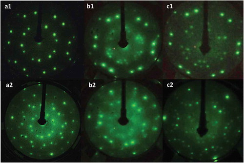
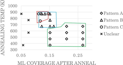
The () LEED spots of the Ni(111) substrate gradually became faint with the deposition of P and completely disappeared at the P saturation coverage. Approximately 0.24 ML of P was deposited, and the surface was annealed to chosen temperatures (573–873 K); three types of LEED patterns designated as pattern A, pattern B, and pattern C were observed, as shown in .
Figure 1. Photographs of LEED images of post annealed surfaces of P dosed onto the Ni(111) surface. a1, a2: pattern A which was formed after 0.26 ML P was deposited on Ni(111) heated at 373 K. b1, b2: images of a series of patterns referred to as pattern B (coverage was 0.15 ML and annealing temperature was 873 K for less than 30 s). c1, c2: pattern C (coverage was 0.12 ML and annealing temperature was 873 K for 10 min). Acceleration energies were 40 eV for a1 and b1, 32 eV for c1, respectively. Acceleration energies for a2, b2 and c2 were 80, 75 and 70 eV, respectively.
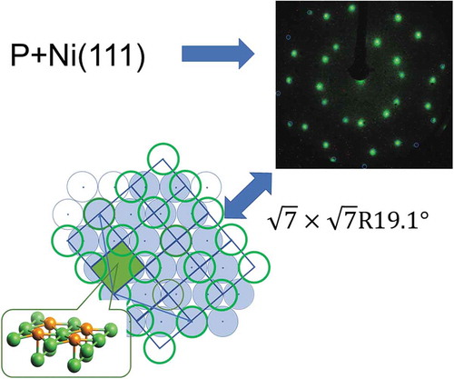
We deposited 0.26 ML P on Ni(111) at 373 K, we obtained Pattern A. Pattern A was consistent with a R19.1° diffraction pattern, which had previously been reported on Ni(111) [Citation26]. shows a
R19.1° structure drawn in LEEDPat4.2 [Citation59] with its commonly used reciprocal lattice unit vectors.
and
were the Ni(111) surface lattice unit vectors while
and
were the overlayer lattice unit vectors. The structure was composed of two domains, which had a mirror symmetry relation with each other as shown in . The 12 spots appeared around (0,0).
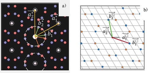
Figure 2. (a) LEED pattern with the reciprocal lattice unit vectors. Red and blue short vectors indicate different domains. Dashed and dot-dashed circles indicate the inner circle around (0,0) and the one around (0, −1), respectively. (b) the real space substrate lattice and its lattice unit vectors (
. Blue and red points indicated the lattice associated with
for two different domains, respectively.
were overlayer lattice unit vectors.
) shows LEED pattern B after annealing at 873 K for 30 sec. Pattern B had LEED spots that corresponded well with those of R19.1° especially around (n,m) (n or m = 1,-1). The spots around (0,0) (on the dashed line in )) were split into three spots compared to pattern A, indicating that pattern B had a unit cell incommensurate to the substrate unit cell. These groups of three spots around (0,0) were always weak and diffuse. Consequently, 12 sets of three split spots appeared around (0,0). We believe that pattern B corresponds to a newly reported structure.
At higher temperatures that ranged from 773 and 873 K, pattern C appeared where 6 sets of 5 spots were found in the inner circle. The -like spots were stronger around (n,m) (n or m = 1,–1). This pattern C corresponds to the one observed previously on P on Ni(111) prepared by PH3 deposition [Citation25]. Note that the coverage decreased with temperature. When the initial coverage of P was 0.24 ML, 873 K annealing produced pattern C and reduced the P coverage to 0.12 ML, probably due to the diffusion into bulk Ni or evaporation from the surface.
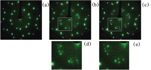
In order to see the relation between these patterns, we carried out subsequent heating. ) shows the R19.1° after 573 K annealing. When the sample was heated to 773 K, pattern B was observed, as shown in ). ) has blue open circles which serve as a visual guide and correspond to the
R19.1° spots seen in ). These spots were slightly shifted in the direction of the substrate reciprocal lattice unit vector, as shown in ). In addition, their positions were varied with the annealing temperature and duration time as shown in ) where the sample was heated at 773 K for another 10 min. The difference between and was the location of the three split spots. The three split spots were expanded, and two sets of the neighboring three split spots moved closer to each other with increased annealing time. Pattern B appeared to be a transient structure. Further expansion of the three split spots transformed the two sets of three split spots into one set of 5 spots observed in pattern C. These similarities and continuous changes indicated that the unit cells of pattern A, pattern B and pattern C were closely related.
Figure 3. LEED patterns for P/Ni (111) (initial coverage was 0.24 ML) (a): Annealed at 573 K for 10 min, pattern A appeared; (b) After sequential annealing at 773 K for 10 min, we obtained pattern B; (c) After further annealing at 773 K for 10 min, the LEED corresponding to pattern B appeared but spots changed compared to the previous one (b). (d) and (e) are expanded images of (b) and (c), respectively. The separation of the three split spots became larger in (c) and (e). The small blue circles in (a), (b), and (c) indicated the spot positions.
shows the phase diagram of P on Ni(111). Here, each sample was annealed at the designated temperatures. The coverages reported were measured by AES after the annealing and LEED measurements. For coverages less than 0.08 ML, we could not detect a LEED pattern since the surface remained amorphous. For coverages greater than 0.11 ML, the structure started to appear above 373 K. If the sample was heated above 673 K, we observed pattern B where the
spots were split into three. Pattern B is a transient structure, and the spot positions gradually changed with further annealing. Finally, when the sample was annealed above 773 K–873 K, pattern C was observed. Since pattern B was a transient state from pattern A to pattern C, we had overlapping areas of pattern B and pattern C where both pattern formations were highly dependent on the dosing amount, annealing temperature, and annealing time.
Figure 4. Phase diagram showing conditions for the three observed patterns. P coverages below 0.08 ML did not produce clear LEED patterns after annealing. Coverages were determined by AES after LEED imaging was complete.
Discussion
The overlayer lattice unit vector
and
were expressed by the substrate vectors,
and
as
Or
This can be graphically shown as in . The reciprocal lattice unit vector was written as
Saidy et al. produced a hexagonal unit cell to explain the structure [Citation26]. In their model structure, 3 Ni atoms were replaced with 3 P atoms. The maximum coverage of P was thus 0.57 ML. However, this hexagonal unit cell could not explain the three split spots in pattern B. To observe the three split spots, the breakdown of 3 fold rotational symmetry is necessary. We could reproduce the three split spots in the inner circle around (0,0) if the angle between the overlayer lattice unit vectors
and
was set to 130° and the angle between the overlayer lattice unit vector and the substrate (
and
) was set to −9.1° instead of −19.1°. As in pattern C, 6 sets of five spots could be seen by the rotation of the overlayer by 9.1° where the angle between
and
became 0°. This lattice unit vector allowed us to create the incommensurate surface structure by breaking down the three-fold rotational symmetry. Unfortunately, this approach also had a fatal problem in that there was no agreement between the calculated and observed spots around (m,n) (m or n = −1,1). This lack of model agreement occurred because the spots on the inner circle around the (0,0) spot were used for the reciprocal lattice unit vectors. It is not necessary to select the spots around (0,0) as the reciprocal lattice unit vectors because electron diffraction suffers strongly from multiple scattering [Citation60]. Since the spots around (m,n) (m or n = −1, 1) appeared stronger in pattern B and pattern C, these spots could be regarded as the reciprocal lattice unit vectors. The spots around (0,0) appeared as a result of multiple scattering. Based on this idea, we reinterpreted the
pattern. We previously proposed the structure for pattern C as shown in based on extended x-ray absorption fine structure (EXAFS) analysis [Citation25], where the topmost two layers of Ni were reconstructed to a rectangular unit cell. The P was adsorbed above the center of the rectangular unit. If we reproduced the
19.1° based on this rectangular model, we could connect pattern A (
19.1°) and pattern C. After trial and error, we found the rectangular unit cell could indeed be well fit to the hexagonal
19.1°. First, we selected the surface reciprocal lattice vectors from the spots on the circle around (m,n)(m or n = −1, 1) shown as
and
in ).
Figure 5. Model structure proposed for pattern C [Citation25]. Green spheres are Ni and the orange spheres are P.
![Figure 5. Model structure proposed for pattern C [Citation25]. Green spheres are Ni and the orange spheres are P.](/cms/asset/d48bbb88-4fba-4890-a20b-381c6d241161/tsta_a_1598239_f0005_oc.jpg)
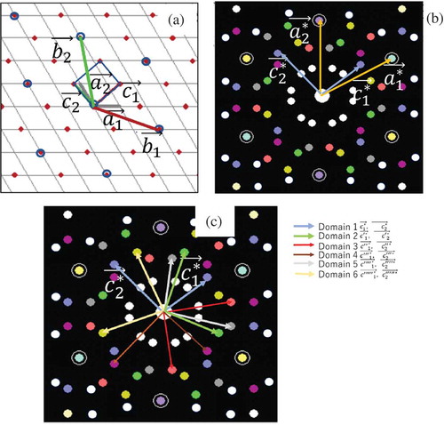
Figure 6. (a) The rectangular overlayer lattice points (red) with lattice vectors (,
). The blue circles are the lattice points of the
R 19.1 structure with lattice vectors (
,
). (b) reciprocal space of (a). The white spots indicate multiple scattering. (c) Lattice unit vectors 6 domains.
The relationship between ) and (
,
) was
The required for the
structure were the unit cell vectors for which both the
and
lattices were commensurate as shown in
The spots around the (0,0) appeared as the result of multiple scattering events in the overlayer and the substrate lattices that reproduced the LEED patterns as shown in ). For example, is created by
in ). Note that the multiple scattering spots of the other domains appeared at the same position. For example, the multiple scattering spots of
in the second domain(Domain 2 of ))and of
in the third domain (Domain 3 of )) gave the same spot. In other words, the spots around the (0,0) were triply degenerated spots. This meant when the rectangular unit vectors were slightly deformed, these spots were split into 3 spots, corresponding to pattern B.
Thus, the rectangular unit cell and multiple scattering events can rationally explain the ° structure and its continuous transition to patterns B and C. Moreover, the strong spots in pattern B and pattern C are understood by the reciprocal lattice unit vector, although further calculations are necessary to completely reproduce all of the spots in pattern B and pattern C.
In the literature, the is usually interpreted in terms of a hexagonal overlayer. In the LEED analysis of
of P/Ni(111), 4 surface Ni atoms out of 7 were replaced with 4 P atoms to produce the mixed overlayer of Ni and P [Citation26]. The
overlayer for S adsorbed on Cu(111) [Citation61,Citation62], Rh(111) [Citation63–Citation65] and Pd(111) [Citation66,Citation67] had similar structures, maintaining the hexagonal unit cell. The rectangular lattice structure we propose is unique and explains the relationship between the
structure and the two incommensurate structures of pattern B and pattern C. In the literature we found one other example of the formation of an overlayer with a different lattice system. This example was the
pattern on Ni(111), where the surface overlayer had a square lattice [Citation24]. S was adsorbed on the square-reconstructed Ni surface to increase the number of S-Ni bonds.
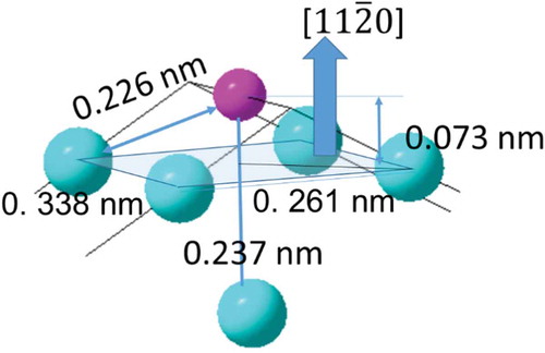
Hereinafter, we continue to discuss the possible local structure around P based on the rectangular reconstruction. We have proposed a rectangular unit cell for pattern C, as shown in , which has dimensions 0.275 × 0.349 nm. P adsorbs on the center of the reconstructed Ni rectangular unit. If a similar unit cell is formed in pattern A, or °, the rectangular structure has size 0.284 × 0.329 nm. In this model structure the maximum coverage of P should be 4/7 ML. This structure can be related to the local structure found in the (
) surface of the Ni2P crystal, which has a rectangular 0.261 × 0. 338 nm lattice. Each corner of this rectangular local structure has Ni atoms, as shown in . P is situated at the Ni 4-fold hollow site. Therefore the rectangular unit of the
structure has a similar local structure to Ni2P.
Figure 7. Part of the crystal structure unit of Ni2P. The large blue and small purple sphere represent Ni and P atoms, respectively. The blue rhombus corresponds to the () plane.
Further reconstructions to pattern B and C might occur to produce more stable structures. Pattern B might be the transient structure from the structure to the structure of pattern C. In order to measure the actual unit cell dimension and to confirm the definite conclusions, we need further calculations and experiments on the
structure of P/Ni(111) using atomic scale STM and EXAFS.
Conclusions
We have found that overlayer structures formed during the adsorption of P on Ni(111) depends on the coverage, the annealing temperature and time. When the sample is heated between 373 K and 673 K, the reconstructed structure is created. Annealing at temperatures above 673 K leads to the formation of pattern B, where the spots in the
pattern are split into three spots. The degree of separation and position of the three spots continue to change with temperature and annealing time. At higher temperatures, pattern C is produced where every two of the twelve sets of the three split spots in pattern B merge to give a pattern with six sets of five spots each. We have proposed a new interpretation of the
structure based on a rectangular unit cell, which can explain the successive changes to pattern B and pattern C. The rectangular unit is similar to the local structure of P on the Ni2P
plane, and it can be regarded as the model structure for the Ni2P surface.
Acknowledgments
The authors express their gratitude to the South Carolina Smart State Center of Economic Excellence for Strategic Approaches to the Generation of Electricity (SAGE), and the National Science Foundation grant DGE 1250052.
This collaboration was carried out under the friendship contract between ICAT Hokkaido University and the Department of Chemical Engineering, University of South Carolina. The work is supported by the CREST-JST project ‘Innovative Catalyst’. The GaP evaporator was constructed by ICAT technical division. We used an open software LEEDPat4.2 provided by the Fritz-Haber-Institute, Berlin (http://www.fhi-berlin.mpg.de/KHsoftware/LEEDpat/). The evaporation systems were constructed by the technical support team of Institute for Catalysis, Hokkaido University.
Disclosure statement
No potential conflict of interest was reported by the authors.
Additional information
Funding
References
- Van Hove MA, Hermann K, Watson PR. The NIST Surface Structure Database-SSD version 4. 2002;58:338–342.
- Somorjai GA. Introduction to surface chemistry and catalysis. New York: Wiley Interscience; 1993.
- Wang L-Q, Hussain Z, Huang Z, et al. Surface structure of√ 3×√ 3 R30° Cl/Ni (111) determined using low-temperature angle-resolved photoemission extended fine structure. Phys Rev B. 1991;44:13711.
- Erley W, Wagner H. Chlorine adsorption on Ni(111). Surf Sci. 1977 August 01;66(1):371–375.
- Takata Y, Sato H, Yagi S, et al. Site-selective adsorption of Cl atoms on Ni(111) studied by back-reflection X-ray standing-wave method. Surf Sci. 1992;265:111–117.
- Funabashi M, Yokoyama T, Takata Y, et al. Surface Structure of Cl/Ni(111) determined by surface EXAFS spectroscopy and soft X-ray standingwave method. Surf Sci. 1990;242:59.
- Wu Y, Mitchell K. A refined LEED structural determination for the surface designated Ni (111)–(2×2)–S. Can J Chem. 1989;67:1975–1979.
- Warburton D, Wincott P, Thornton G, et al. Incorporation of sulphur into the (111) surface of nickel? Surf Sci. 1989;211:71–81.
- Fauster T, Dürr H, Hartwig D. Determination of the geometry of sulphur on nickel surfaces by low-energy ion scattering. Surf Sci. 1986;178:657–666.
- Andrews D, Woodruff D. The local adsorption site for sulphur on Ni {111} in the low coverage lattice gas. Surf Sci. 1984;141:31–39.
- Capehart TW, Seabury C, Graham G, et al. Coverage dependent adsorption site for sulfur on Ni (111). Surf Sci Lett. 1982;120:L441–L446.
- Marcus P, Demuth J, Jepsen D. Determination of the structure of ordered adsorbed layers by analysis of LEED spectra. Surf Sci. 1975;53:501–522.
- Demuth J, Jepsen D, Marcus P. Crystallographic dependence of chemisorption bonding for sulfur on (001), (110), and (111) nickel. Phys Rev Lett. 1974;32:1182.
- Gardin DE, Batteas JD, Van Hove MA, et al. Carbon, nitrogen, and sulfur on Ni(111): formation of complex structures and consequences for molecular decomposition. Surf Sci. 1993;296:25–35.
- Yamada M, Hirashima H, Kitada A, et al. Three-Ni-atom cluster formed by sulfur adsorption on Ni (1 1 1). Surf Sci. 2008;602:1659–1668.
- Zharnikov M, Weinelt M, Zebisch P, et al. Holography of clean and sulphur-covered Ni (111) using multiple wave number photoelectron diffraction patterns. Surf Sci. 1995;334:114–134.
- Bäcker R, Hörz G. Scanning tunneling microscopy of carbon-and sulfur-induced modifications of Ni (111) and Ni (110) surfaces. Vacuum. 1995;46:1101–1104.
- Maurice V, Kitakatsu N, Siegers M, et al. Low-coverage sulfur induced reconstruction of Ni (111). Surf Sci. 1997;373:307–317.
- Mullins D, Huntley D, Overbury S. The nature of the sulfur induced surface reconstruction on Ni (111). Surf Sci. 1995;323:L287–L292.
- Erley W, Wagner H. Sulfur poisoning of carbon monoxide adsorption on Ni (111). J Catal. 1978;53:287–294.
- Delescluse P, Masson A. Diffuse scattering in RHEED induced by linear disorders of sulphur segregated on nickel (111) surface. Surf Sci. 1980;100:423–438.
- Ku Y-S, Overbury SH. Structure analysis of S adsorbed on Ni(111) by low energy Li+ ion scattering. Surf Sci. 1992;276:262–272.
- Ruan L, Stensgaard I, Besenbacher F, et al. Observation of a missing-row structure on an fcc (111) surface: the (5√ 3 × 2) S phase on Ni (111) studied by scanning tunneling microscopy. Phys Rev Lett. 1993;71:2963.
- Kitajima Y, Yokoyama T, Ohta T, et al. Surface EXAFS and XANES studeis of 5 √3x2 S/Ni(111): a pseudo c(2x2) S/Ni(100) model with surface reconstruction. Surf Sci. 1989;214:L261.
- Asakura K, Konishi S, Ohta T, et al. EXAFS studies on the adsorption strucutres of P/Ni(111). Jpn J Appl Phys. 1993;32-2:359–361.
- Saidy M, Zhou MY, Mitchell KAR. Tensor LEED analysis for the Ni(111)–(√7 × √7)R19.1°–P surface structure: comparison with other √7 systems. Surf Interface Anal. 1999;28:84–91.
- Rundqvist S. X-ray Investigations of Mn3P, Mn2P, and Ni2P. Acta Chem Scand. 1962;16:992–998.
- Oyama ST. Novel catalysts for advanced hydroprocessing: transition metal phosphides. J Catal. 2003;216:343–352.
- Robinson WRAM, Jnm VG, Korányi TI, et al. Phosphorus promotion of Ni(Co)-containing Mo-free catalysts in quinoline hydrodenitrogenation. J Catal. 1996;161:539–550.
- Wang X, Clark P, Oyama ST. Synthesis, characterization, and hydrotreating activity of several iron group transition metal phosphides. J Catal. 2002;208:321–331.
- Li K, Wang R, Chen J. Hydrodeoxygenation of anisole over silica-supported Ni2P, MoP, and NiMoP catalysts. Energy Fuels. 2011;25:854–863.
- Voo G, de Souza PM, Cabioc‘H T, et al. Effect of P/Ni ratio on the performance of nickel phosphide phases supported on zirconia for the hydrodeoxygenation of m-cresol. Catal Commun. 2018. DOI:10.1016/j.catcom.2018.09.015.
- Berenguer A, Sankaranarayanan TM, Gomez G, et al. Evaluation of transition metal phosphides supported on ordered mesoporous materials as catalysts for phenol hydrodeoxygenation. Green Chem. 2016;18:1938–1951.
- Gonçalves VOO, de Souza PM, Da Silva VT, et al. Kinetics of the hydrodeoxygenation of cresol isomers over Ni2P/SiO2: proposals of nature of deoxygenation active sites based on an experimental study. Appl Catal B Environ. 2017;205:357–367.
- Shi Y, Zhang B. Recent advances in transition metal phosphide nanomaterials: synthesis and applications in hydrogen evolution reaction. Chem Soc Rev. 2016;45:1529–1541.
- Popczun EJ, McKone JR, Read CG, et al. Nanostructured nickel phosphide as an electrocatalyst for the hydrogen evolution reaction. J Am Chem Soc. 2013;135:9267–9270.
- Kawai T, Bando KK, Lee YK, et al. EXAFS measurements of a working catalyst in the liquid phase: an in situ study of a Ni2P hydrodesulfurization catalyst. J Catal. 2006;241:20–24.
- Bando KK, Wada T, Miyamoto T, et al. Combined in situ QXAFS and FTIR analysis of a Ni phosphide catalyst under hydrodesulfurization conditions. J Catal. 2012;286:165–171.
- Wada T, Bando KK, Miyamoto T, et al. Operando QEXAFS studies of Ni2P during thiophene hydrodesulfurization: direct observation of Ni-S bond formation under reaction conditions. J Synchrotron Radiat. 2012;19:205–209.
- Wada T, Bando KK, Oyama ST, et al. Operando observation of Ni2P structural changes during catalytic reaction: effect of H2S pretreatment. Chem Lett. 2012;41:1238–1240.
- Edamoto K, Inomata H, Shimada T, et al. Valence and core-level photoelectron spectroscopy study of the electronic structure of Ni2P(0001). e-J Surf Sci Nanotechnol. 2009;7:1.
- Edamoto K, Nakadai Y, Inomata H, et al. Soft XPS study of Ni2P(0001). Solid State Commun. 2008;148:135.
- Ariga H, Kawashima M, Takakusagi S, et al. Density function theoretical investigation on the Ni3PP structure and its hydrogen adsorption property of Ni2P(0001) surface. Chem Lett. 2013;42:1481–1483.
- Moula MG, Suzuki S, Chun WJ, et al. The first atomic-scale observation of a Ni2P(0001) single crystal surface. Chem Lett. 35:90–91. doi: 10.1246/cl.2006.90
- Liu P, Rodriguez JA, Asakura T, et al. Deslufrization reactions on Ni2P(0001) and α-Mo2C(001) surfaces: complexrole of P and C sites. J Phys Chem B. 2005;109:4575.
- Hernandez AB, Ariga H, Takakusagi S, et al. Dynamical LEED analysis of Ni2P (0001)-1 × 1: evidence for P-covered surface structure. Chem Phys Lett. 2011;513:48–52.
- Guo D, Nakagawa Y, Ariga H, et al. STM studies on the reconstruction of the Ni2P(101b0) surface. Surf Sci. 2010;604:1347–1352.
- Edamoto K, Inomata H, Ozawa K, et al. Electronic structure of the Ni2P(101b0) surface: angle-resolved photoemission study. Solid State Commun. 2010;150:1120–1123.
- Imanishi S, Munakata S, Kakefuda Y, et al. Characterization of Ni2P(10-10): soft X-ray photoelectron spectroscopy study. e-J Surf Sci Nanotechnol. 2012;10:45–49.
- Edamoto K, Inomata H, Yasuno N, et al. Angle resolved and resonant photelectron spectroscopy study of Ni2P(101b0) single crystal surface. Hyomen Kagaku. 2010;31:324.
- Suzuki S, Moula GM, Miyamoto T, et al. Scanning tunneling microscopy and photoemission electron microscopy studies on single crystal Ni2P surfaces. J Nanosci Nanotechnol. 2009;9:195–201.
- Kinoshita K, Simon GH, Konig T, et al. A scanning tunneling microscopy cbservation of (√3 x√3) R30 reconstruction Ni2P (0001). Jpn J Appl Phys. 2008;47:6088–6091.
- Yuan Q, Ariga H, Asakura K. An investigation of Ni2P single crystal surfaces: structure, electronic state and reactivity. Topics Catal. 2015;58:194–200.
- Contreras-Mora J, Ariga-Miwa H, Takakusagi S, et al. Phosphorous diffusion through Ni2P—low energy diffusion path and its unique local structure. J Phys Chem C. 2018;122:6318–6322.
- Song JD, Kim JM, Lee YT. Molecular beam epitaxial growth of high-quality InP/InGaAs/InP heterostructure with polycrystalline GaAs and GaP decomposition sources. Jpn J Appl Phys. 2000;39:L347.
- Goh KEJ, Oberbeck L, Butcher M, et al. Comparison of GaP and PH3 as dopant sources for STM-based device fabrication. Nanotechnology. 2007;18:065301.
- Mondry M, Caine E, Kroemer H. A GaP decomposition source for producing a dimer phosphorus molecular beam free of gallium and tetramer phosphorus. J Vac Sci Technol A. 1985;3:316–318.
- Kiskinova M, Goodman DW. Modification of chemisorption properties by electronegative adatoms: H2 and CO on chlorided, sulfided, and phosphided Ni(100). Surf Sci. 1981;108:64–76.
- Herman KE, Van Hove MA. LEEDpat, version 4.2. 2014. http://www.fhi-berlin.mpg.de/KHsoftware/LEEDpat/
- Ertl G, Küppers J. Low energy electrons and surface chemistry. Weinheim, Federal Republic of Germany; Deerfield Beach, FL, USA: VCH; 1985.
- Saidy M, Mitchell KAR. Tensor LEED analysis for the Cu(111)-(7×7)R19.1°-S surface structure. Surf Sci. 1999;441:425–435.
- Yoshinori K, Yasutaka T, Hitoshi S, et al. Surface structure of (√7×√7) R19.1°S/Cu(111) studied by surface EXAFS and back-reflection X-ray standing-wave method. Jpn J Appl Phys. 1993;32(S2):377.
- Liu W, Wong KC, Mitchell KAR. LEED crystallographic analysis for the Rh(111)-(√7 ×√7)R19.1°P surface structure. Surf Sci. 1997;372:312–322.
- Liu W, Wong KC, Mitchell KAR. Novel surface structure: Rh(111)-(√7 × √7)R19.1°P. J Am Chem Soc. 1995;117:12344–12345.
- Shard AG, Dhanak VR, Muryn CA. SEXAFS and NIXSW investigation of the Rh(111)-(7×7)R19.1°-P surface. Surf Sci. 1999;433–435:267–271.
- Forbes JG, Gellman AJ, Dunphy JC, et al. Imaging of sulfur overlayer structures on the Pd(111) surface. Surf Sci. 1992;279:68–78.
- Grillo ME, Stampfl C, Berndt W. Low-energy electron-diffraction analysis of the (√7 × √7)R19.1°-S adsorbate structure on the Pd(111) surface. Surf Sci. 1994;317:84–98.