
 ?Mathematical formulae have been encoded as MathML and are displayed in this HTML version using MathJax in order to improve their display. Uncheck the box to turn MathJax off. This feature requires Javascript. Click on a formula to zoom.
Abstract
This article presents a wideband metamaterial absorber (WMMA) for the visible and near-infrared (NIR) region application. The proposed metamaterial absorber comprises three layers of sandwiched (metal-dielectric-metal) model based on Nickel-Polyamide-Nickel. The multiple resonators on top layers achieve an average absorption of 98.16% over a range from 380 to 2300 nm with a compact unit cell size of 100 × 100 × 42 nm3. The designed WMMA shows 99% perfect absorption for a large bandwidth of 685 nm. Considering its wideband absorption, the physical absorption phenomenon was also explained in terms of the proposed WMMA's surface electric field, magnetic field, and current distribution. Also, the effects of materials and structural parameters on absorption performance with a FOM have been studied. The absorption performance is analysed with various polarization angles to demonstrate polarization insensitivity. The designed WMMA shows the absorption of >70% at large incident angles of 70°. The perceptible contribution of this WMMA is large unity absorption bandwidth at visible to NIR region with high incident angle stability, polarisation insensitivity, thermal robustness of the constituting metal and simple nanostructure geometry. Therefore, the proposed WMMA has good potential in sensors, thermal emitters, photodetectors, and absorber applications.
1. Introduction
Metamaterials are an exciting new technology that can be utilised to alter electromagnetic waves at deep subwavelength scales. The state-of-the-art research demonstrates that metamaterials are widely used for various applications like antenna,[Citation1,Citation2] sensing,[Citation3–5] stealth technology,[Citation6] energy harvesting,[Citation7] communication,[Citation8] EMI shielding,[Citation9] reflect array,[Citation10] and absorber[Citation3,Citation11–13] etc. Above all, metamaterial absorbers (MMA) are becoming very prominent for multipurpose applications, such as THz absorption,[Citation14,Citation15] imaging[Citation16] and biosensor,[Citation17] etc. The MMA concept is developed on customised metal–dielectric–metal interface for creating artificial meta-atoms, which can enhance the absorption intensity of the MMA in visible and infrared region applications. Within this context, the metamaterial absorber can be configured in various shapes and sizes to absorb a specific frequency or a range of frequencies. Metamaterial absorbers are classified into two categories based on their absorption bandwidth: narrowband[Citation18–22] and wide-band absorbers.[Citation8,Citation12,Citation22–25] Narrowband MMA absorbs a small portion of the visible or infrared (IR) regions and find useful in thermal emission manipulation, nano-antennas, sensors, and resonators based on absorption bandwidth.[Citation8,Citation17,Citation21,Citation26–28] On the other hand, the concept of wideband MMA has recently been adopted by piling of metallic and dielectric material layers,[Citation8,Citation17,Citation20,Citation24,Citation25,Citation29] combination of different unit cells with perfect absorption peaks,[Citation30,Citation31] and use of multiple resonators,[Citation32] etc. However, these stacking techniques depict a tiny number of feasible resonance combinations, making high cost and design complexity. Therefore, there is a great need to develop broadband, compact, and highly efficient metamaterials for absorption applications. Recently, numerous researchers have been performed to achieve wideband absorption characteristics in the visible to infrared wavelength using different metamaterial structure configurations. In,[Citation17] multiple ellipse-shaped metamaterial is proposed for visible region absorption, which attains polarisation-sensitive absorption over 90% for only 350 nm bandwidth (400–750 nm wavelength). Consequently, a star-shaped polarization-insensitive metamaterial is proposed for a visible region with near-perfect absorption from 389.34 to 697.19 nm.[Citation21] In,[Citation20] a polarisation-insensitive multilayer metamaterial structure with above 90% absorption from 300 to 680 nm is investigated, where angular angle stability is achieved up to 50° only. Different shapes like, cross, rectangular, and cylindrical are employed in multilayer metamaterial structure which achieve absorption ≥90% for visible and partially covered NIR with angular stability up to 50°.[Citation23,Citation25,Citation33] Subsequently, in,[Citation8] a multi-layered conical frustums-shaped absorber is developed, and the structure achieved polarisation-insensitive absorption ≥90%, from 480 to 1480 nm. A hexagonal ring array based ultra-wideband plasmonic absorber on fractals is employed to improve the absorption and incident angle stability up to 60°.[Citation32] A visible-to-infrared absorber is designed in,[Citation34] the structure is polarization sensitivity. A gear shape MMA is presented in;[Citation35] however, it partially covers the visible region. Based on the aforementioned discussion, designing a wideband MMA with high angular stability and compact unit cell size is very challenging due to the inherent relation between bandwidth and the number of layer architecture. Therefore, a polarization-insensitive, high oblique incident angle stable, compact size MMA is highly desirable for visible to infrared regions.
This paper proposed a compact Ni-PI-Ni-based simple MMA structure for visible and NIR regions, which shows average absorption over 98% for the wavelength range of 380–2300 nm for Ni-based multiple resonators on top, followed by a Ni layer on the bottom and polyimide use as a substrate layer. The symmetrical structure achieves polarization insensitivity, and the low periodicity of the unit cell achieves oblique incident angle stability up to 70°.
2. Design methodology
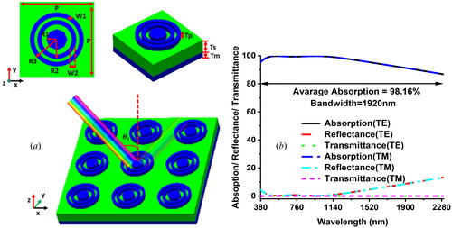
(a) shows the schematic layout of the proposed WMMA. The WMMA comprises three layers of Ni–PI–Ni structure. Ni-based octagonal and two-ring resonators are placed on the top layer, polyimide (PI) is used as a substrate layer, and full-plane Ni is used on the bottom. Ni is chosen due to its excellent chemical stability, low cost, and high melting point.[Citation34,Citation36–38] The electrical and thermal conductivity of the used Nickel material is 1.44 × 10^7 S/m and 91 W/k/m.[Citation37] on the other hand, the lossy substrate PI is chosen due to its thermal stability, withstand temperatures of up to 350 °C without losing structural integrity.[Citation39,Citation40] The periodicity of the unit cell is represented by ‘P', which is only 100 nm. The inner octagonal resonator has a radius of R1 = 10 nm, and the middle and outer circular rings have a radius of R2 = 26 nm and R3 = 36 nm, respectively. The width of the circular ring resonators is W2 = 0.5 nm. The thickness of the top nickel layer is ‘Tp = 8 nm’, and the top layer is deposited on a lossy PI-based substrate layer where the substrate layer thickness is ‘Ts’ = 24 nm. The thickness of the bottom layer of this WMMA is ‘Tm = 10 nm'. The CST microwave studio software[Citation41] is utilized for electromagnetic (EM) simulation, EM response and field distribution analysis. The unit cell boundary condition is used in the x and y-axis, and transverse electric (TE) and transverse magnetic (TM) EM waves are applied from the positive to negative z-axis using the Floquet port. The absorption of the proposed WMMA is calculated by EquationEquation (1)(1)
(1) .[Citation42] The reflectance, transmittance, and absorption are depicted in (b). The transmitted coefficient is almost zero for the entire operational wavelength because of the complete Ni-based ground plane. The average absorption of 98.16% from 380 to 2300 nm with a bandwidth of 1920 nm. Moreover, due to the design’s structural symmetry, the absorption characteristic is homogeneous for TE and TM mode polarization.
Figure 1. (a) The schematic of the proposed WMMA, (b) simulated absorption, reflection, and transmission of the proposed WMMA.
The absorption mechanism of the proposed WMMA can be understood from design evolutions. shows the consecutive design stages of the proposed WMMA structure, and illustrates the corresponding absorption characteristics. In stage 1, a single octagonal resonator initially achieves low average absorption of 73.54% for visible and infrared regions (380–2300 nm). After that, by adding one circular shape ring, the absorption increases significantly at the NIR wavelength due to the coupling capacitance between the octagonal and the additional inductivity by the circular ring. Finally, an additional circular ring is placed, resulting in additional coupling capacitance and inductance, increasing the average absorption to 98.16% for 380–2300 nm.[Citation12] So, the inner resonator is responsible for absorption at lower wavelengths, and the outer resonator contributes to high absorption at higher wavelengths. The coupling effect on the electric field of the proposed WMMA at different stages is presented in . Absorption bandwidth and average absorption of different stages of the proposed WMMA design analogy are listed in .
Figure 2. (a) Different stages of design analogy, and (d) absorption of design stages.
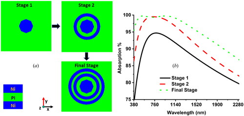
Figure 3. Electric field distribution of proposed WMMA at 1900 nm for different stages.
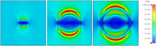
Table 1. Absorption bandwidth and average absorption of different stages of design analogy.
As earlier stated, the absorption is calculated by bellow EquationEquation (1)(1)
(1) ,
(1)
(1)
where A(ω), R(ω) and T(ω) represent the absorption, reflectance and transmittance, respectively. The scattering parameters can be used to express the reflectance and transmittance, as shown in EquationEquation (2)
(2)
(2) :[Citation43]
(2)
(2)
In the above equation, S11(ω) = the reflection coefficient and S21(ω) = the transmission coefficient. The S21(ω is close to zero for this WMMA because the Ni-based bottom layer completely blocks the propagation of EM wave through the structure, so the absorption depends only on S11(ω).
(3)
(3)
The absorption phenomena can be controlled by varying the geometrical shape of the resonators.[Citation44] (a) depicts the absorption spectra of the proposed WMMA with various resonator shapes under normal incidence. The relative absorption bandwidth (BRA) is used to analyse the absorption performance of the WMMA using EquationEquation (4)(4)
(4) and listed in .[Citation45] Where λH and λL are the higher and lower wavelength at 90% absorption
(4)
(4)
Figure 4. (a) Absorption spectra of the proposed WMMA and (b) electric field distribution at 1900 nm with different resonator shapes at normal incidence.
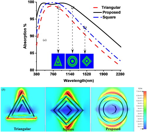
Table 2. Absorption properties of the proposed WMMA structure with different resonator shapes.
As shown in , the proposed circular shape split ring resonator achieves BRA around 135%, indicating a good wideband property and absorption efficiency greater than 90% for a wideband wavelength range of 380–2300 nm. Furthermore, the proposed WMMA structure has an average absorption of 98.16% higher than other shapes for the entire operational bandwidth due to the better coupling effect at circular resonators, as shown in (b). The absorption level can be optimized by adjusting the geometric parameters of the unit cell.[Citation46] To analyse the performance of the proposed design for different design parameters, a figure of merit (FOM) is presented in EquationEquation (5)(5)
(5) .[Citation44] Where Δn = nmax-nmin, nmax = higher wavelength, nmin = lower wavelength.
(5)
(5)
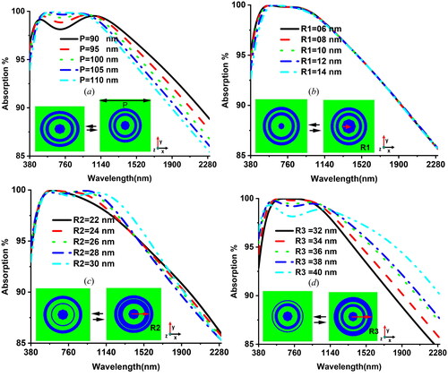
illustrates the effect of structural parameters on absorption characteristics to select the optimum values of the proposed WMMA. In , the surface length dimension "P" is swept from 90 nm to 110 nm with a step of 10 nm. Absorption at higher wavelengths varies noticeably as the surface length dimension changes. For a continuous increment of the "P" value, absorption increases until 100 nm, and after that, the value starts to decrease due to the coupling of two adjacent unit cell structures. Finally, 100 nm is opted for the surface length due to its highest average absorption of 98.16% at the entire operational wavelength range. The top octagonal ring radius "R1" also varies from 6 to 14 nm, presented in . It can be seen that the absorption at the visible region is slightly reduced for the increment of "R1". However, at a 10 nm radius, the visible region’s average absorption is 98.70%. Hence "R1" = 10 nm is adopted for the hexagonal ring radius. Moreover, the width of the ring resonators has a significant effect on absorption. shows absorption characteristics for different values of outer radius “R2” for the middle ring resonator, which is swept from 22 to 30 nm at a 2 nm interval. The variation of “R2” significantly impacts absorption at the mid-range of the operating wavelength. In , the outer radius “R3” of the outer ring resonator is varied from 32 to 40 nm at a 2 nm interval. As the outer radius of the outer ring increases, the absorption level increases in the NIR region; however slightly reduced near 760 nm wavelength. Finally, "R3" = 36 nm is set for the outer ring resonator for its highest average absorption at the desired wavelength. Therefore, it is clear that the dimension of the inner resonator, middle resonator and outer resonator significantly impacts the visible, middle operating wavelength and NIR region, respectively.
Figure 5. Absorption characteristics for various geometric parameters of the WMMA, including (a) surface length, (b) octagonal ring radius, (c) middle ring outer radius, and (d) outer ring outer radius.
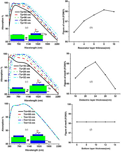
The effect of different layer thicknesses on absorption properties and corresponding FOM are shown in . When top resonator thickness "Tp" is increased, the absorption level rises for the near-infrared region, but the absorptivity level reduces at the visible region, depicted in . For "Tp" = 10 nm, both absorption and the FOM reach an optimum level, but absorption is reduced in the visible range, as illustrated in . Therefore “Tp" = 8 nm is set as the final value. shows absorptions for different substrate "Ts" values from 16 nm to 32 nm. The absorption level increases with the increment of "Ts" at the NIR region but is reduced at the visible wavelength. The FOM for “Ts" is shown in , which indicates the highest absorption value reaches at “Ts" = 24 nm. In addition, the bottom layer thickness "Tm" is swept from 6 to 14 nm at a 2 nm increment, and corresponding absorptions are shown in . which shows similar absorption due to the effective blocking of EM wave through the structure by Ni material, and the lowest values of nickel thickness are above the skin depth.[Citation47] Also, the corresponding FOM value for different bottom layers stays constant, as illustrated in .
Figure 6. Absorption characteristics for (a) resonator layer thickness, (c) substrate layer thickness, (e) bottom layer thickness and Figure of merit for (b) resonator layer thickness, (d) substrate layer thickness and (f) bottom layer thickness of the WMMA.
3. Result analysis and discussion
3.1. Impedance matching and metamaterial properties
The impedance matching condition is essential to justify the absorption performance of an MMA. A perfect impedance match yields a reflection of zero.,[Citation47] which can be understood from EquationEquation (6)(6)
(6) . Where Zr is the WMMA's relative impedance, and Zₒ = 377Ω is the free space impedance. The reflection will be its least value for the condition of Zr ≈ Zₒ. So, unity absorption A(ω) will achieve from EquationEquation (3)
(3)
(3) [
] for zero reflection.
(6)
(6)
(7)
(7)
The relative impedance of the structure depends on the relative permittivity (εr) and permeability (μr), as indicated in EquationEquation (7)(7)
(7) .[Citation48] The metamaterial properties “εr” and “μr” are retrieved from the scattering parameters of the structure using EquationEquation (8)
(8)
(8) ,[Citation48]
(8)
(8)
where,
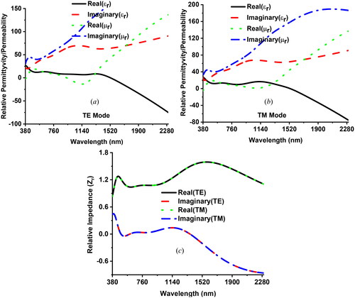
k is the wavenumber, c = velocity and d = Substrate height. The real and imaginary scattering parameter values are utilized to calculate the “εr” and “μr”. shows the retrieved metamaterial property (relative permittivity and permeability) for both TE and TM mode, where a negative permittivity value is achieved at the NIR region. The overall “εr” and “μr” achieves near unity value of the real part and zero value of the imaginary part for the relative impedance (Zr) shown in (c).
Figure 7. Relative permittivity and relative permeability for (a) TE mode, (b) TM mode and (c) Relative Impedance of the proposed WMMA.
3.2. Polarization angle insensitivity and incident angle stability
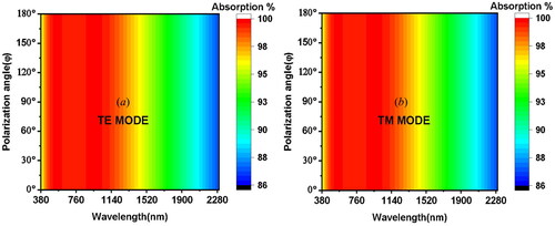
Polarisation insensitivity is one of the most important features of an MMA, which shows constant absorption for different polarized incident EM waves.[Citation20,Citation21] The polarization insensitivity of the proposed WMMA is achieved by rotational symmetrical geometry. shows the proposed WMMA's absorption property for different polarisation angles at TE and TM modes, which exhibit uniform absorption characteristics.
Figure 8. Absorption characteristics of the proposed WMMA in different polarisation angel for (a) TE and (b) TM mode.
The stable absorption at different obliquity of incidence angles is another important factor for designing the efficient MMA because the incident angles have a significant impact on the reflection coefficient of MMA, which is represented by EquationEquations (9)(9)
(9) and Equation(10)
(10)
(10) for TE and TM modes, respectively.[Citation49]
(9)
(9)
(10)
(10)
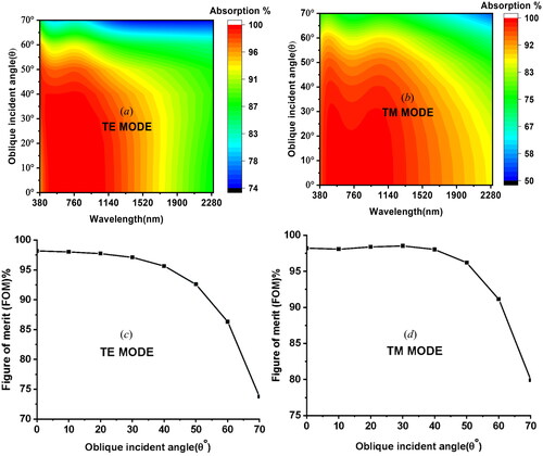
As the oblique incident angle varies, the reflection coefficient will affect the absorption characteristics because, at the oblique incident angle, the phase value of the incoming EM wave varies, which causes the impedance variation of the structure. This impedance variation can be reduced by compact unit cell size.[Citation50] If the MMA impedance mismatch with free space impedance, absorption will be decreased. illustrate the different oblige incident angle effects on the designed WMMA absorption phenomena from 0° to 80° angles at TE and TM modes, respectively. The average absorption is 98–60.70% for different incident angles. At TE mode, for lower incident angles (θ ≤ 0°), the WMMA structure shows average absorption of 90% and up to 70% average absorption for higher incident angles (θ ≤70°). On the other hand, in TM mode, the average absorption is nearly 80% for θ ≤ 70°. show that the FOM value is 98.16% at the normal incident angle. However, at 50° incident angle, the FOM decreases to 92.57% for TE polarization and 96.19% for TM polarisation. Also, The FOM remains greater than 90% for incidences angle up to 50° for TE mode and 60° for TM mode. Besides, FOM also remains 70% for incidence angles up to 70° for TE and TM polarisations, respectively.
Figure 9. The proposed WMMA absorption for (a) TE, (b) TM modes and FOM for (c) TE, and (d) TM modes at the different oblique incident angle.
4. E-field, H-field and surface current distribution
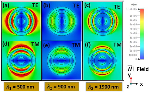
The electromagnetic field and surface current distribution strongly influence absorption properties. and Citation10(e)–(h) show the surface current distribution for TE and TM modes. Due to metal-dielectric-metal interfaces, the surface current is strongly concentrated in the ring resonator and dielectric layers, resulting in localised surface plasmon resonances (LSPRs). The surface current distribution exhibits energy loss, leading to increased broadband absorption.[Citation23] shows the electric field || distribution for TE and TM, respectively. The strong electric field is confined at the edge of the top ring resonator and in the dielectric layer, which creates dipole resonance and resulting absorption increases in the operational wavelength. Furthermore, the |
| field pattern switches when the polarisation changes from TE to TM mode. Also, the magnetic |
| field distribution of the proposed WMMA in is mainly located in the edge of the top ring resonator and PI dielectric layer as like |
| field. The distribution patterns show that the LSPR is excited at the Ni ring resonator and on the PI Substrate layer surfaces for both modes. The direction of propagation changes with the polarisation variations. Most importantly, with a good |
| field and |
| field, as well as a good anti-parallel circulating current, the proposed WMMA is a good absorber for the visible and NIR regions, making it suitable for use in related fields.
Figure 10. Surface current distribution at different wavelengths for the proposed WMMA at TE modes (a) 500 nm, (b) 900 nm, (c) 1900 nm, and TM mode (d) 500 nm, (e) 900 nm, (f) 1900 nm.
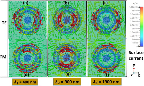
Figure 11. Electric || field distribution at various wavelengths for TE mode (a) 500 nm, (b) 900nm, (c) 1900 nm and for TM mode (d) 500 nm, (e) 900 nm, (f) 1900 nm.
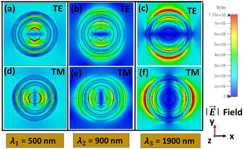
Figure 12. Magnetic || field distribution at various wavelengths for TE mode (a) 500 nm, (b) 900 nm, (c) 1900 nm and for TM mode (d) 500 nm, (e) 900 nm, (f) 1900 nm.
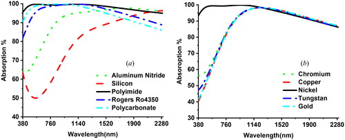
Dielectric material plays a vital role in absorption bandwidth. shows the effect of absorption on aluminium nitride (AIN), silicon, polyimide (PI), rogers R4350, and polycarbonate (PC) dielectric materials for the WMMA. AIN and silicon show good absorption levels of up to 80% for the NIR region, but in the visible region, the absorptivity level is less than 70%. On the other hand, PI, rogers, and PC show good average absorption for the whole operational wavelength: 98.16, 95.11, and 97.25%, respectively. So, polyimide is chosen for the proposed MMA substrate based on its highest average absorption rate, especially in the visible region, where the average absorption is 98.70% greater than other Substrates. Also, it has outstanding thermal stability and optical transparency, and its low thermal expansion coefficient is ideal for use as a substrate in optical and near-infrared region applications. Gold is a high-quality noble metal with excellent resonance selectivity,[Citation51] while Chromium, Nickel, and Tungsten are refractory metals known for their strong light absorption across a wide range.[Citation52] Different refractory metals have varying effects on the performance of metamaterial absorbers due to their distinct dielectric constants.[Citation53] In , refractory metals surpass noble metals as microstructural materials, especially Nickel, which shows a large absorption bandwidth. However, after considering overall absorption and bandwidth, Ni is selected as the preferred microstructure material. This suggests that refractory metals generally offer better and more versatile options for absorber structures compared to precious metals.
Figure 13. The proposed WMMA's absorption characteristics under various (a) dielectric materials and (b) metal.
Similar state-of-the-art research is shown in . In,[Citation17,Citation20,Citation21] absorption above 90% is only achieve in the visible region. In,[Citation8,Citation23,Citation25,Citation33,Citation34] above 90% absorption is achieved for the visible and partially covered NIR region. On the other hand,[Citation8,Citation35] do not cover the complete visible region. Besides, angular stability is only 50° in[Citation16,Citation18,Citation20,Citation30] and 60° in.[Citation14,Citation31,Citation32,Citation54] Furthermore, the structures in[Citation17,Citation34] are polarization sensitive and other works show polarisation insensitivity. The overall thickness and periodicity of the listed MMA in are higher than the proposed WMMA. Besides, the proposed WMMA shows higher average absorption than.[Citation17,Citation20,Citation21,Citation33,Citation35] Finally, the proposed WMMA achieves a broad absorption ≥90% from visible to NIR region from 380 to 2300 nm (average absorption of 98.16%) with a compact and ultra-thin unit cell size of 100 × 100 × 42 nm3. Multiple resonators on the top of the structure realise this increased absorption bandwidth. The low periodicity of the unit cell achieves a high oblique incident angle stability of up to 70°, and the symmetrical design exhibits polarization insensitivity. Therefore, the increased absorption bandwidth with high absorption level over visible to NIR with polarization insensitivity and high oblique incident angle stability compared to others listed MMA makes the proposed WMMA as potential candidate for visible to NIR applications.
Table 3. Comparison of previously reported MMA.
Conclusion
This paper proposed a wideband metamaterial absorber with a unity absorption bandwidth of 682 nm (463–1145 nm) and above 90% absorptions for the visible and NIR regions (380–2300 nm) using multiple ring resonators. An average absorption of 98.16% and relative absorption bandwidth of 135% is achieved over the operating wavelength. The polarisation-insensitivity of the proposed WMMA is achieved by symmetrical geometrical structure. Besides, a high oblique incident angle stability up to 70° is realised for both TE and TM polarisation due to the low periodicity of the unit cell. The parametric investigations, surface current EM field distribution and metamaterial property is analysed to describe the absorption characteristics. Hence, the proposed WMMA is a compelling candidate for visible and infrared applications due to its wider absorption bandwidth, compactness, high-temperature resistance, low material cost, high absorption level, polarization insensitivity, and high oblique incident angle stability.
Author contributions
Abu Hanif: Conceptualization, formal analysis, Methodology, Design, Investigation, Writing—original draft. Mohammad Lutful Hakim: Conceptualization, formal analysis, Methodology, Design, Investigation, Writing—original draft. Touhidul Alam: Supervision, Project administration, Review and editing,Mohammad Tariqul Islam: Supervision, Project administration, Iskandar Yahya: Project administration and Review and editing, Saleh Albadran: Project administration and Review and editing, Md. Shabiul Islam: Project administration and Review and editing, Mohamed S. Soliman: Project administration and Review and editing.
Acknowledgments
The authors are grateful to Universiti Kebangsaan Malaysia.
Disclosure statement
No potential conflict of interest was reported by the author(s).
Data availability statement
The data presented in this study are presented in this article.
Additional information
Funding
References
- Alam, T.; Almutairi, A.F.; Samsuzzaman, M.; Cho, M.; Islam, M.T. Metamaterial array based meander line planar antenna for cube satellite communication. Sci. Rep. 2021, 11, 14087. DOI: 10.1038/s41598-021-93537-6.
- Hakim, M.L.; Alam, T.; Islam, M.T.; Mohd Sahar, N.B.; Jit Singh, M.S.; Alsaif, H.; Soliman, M.S. Metamaterial physical property utilized antenna radiation pattern deflection for angular coverage and isolation enhancement of mm-wave 5G MIMO antenna system. Radiat. Phys. Chem. 2023, 209, 110998. DOI: 10.1016/j.radphyschem.2023.110998.
- Deng, X.; Shen, Y.; Liu, B.; Song, Z.; He, X.; Zhang, Q.; Ling, D.; Liu, D.; Wei, D. Terahertz metamaterial sensor for sensitive detection of citrate salt solutions. Biosensors 2022, 12, 408. DOI: 10.3390/bios12060408.
- Li, Z.; Cheng, Y.; Luo, H.; Chen, F.; Li, X. Dual-band tunable terahertz perfect absorber based on all-dielectric InSb resonator structure for sensing application. J. Alloys Compd. 2022, 925, 166617. DOI: 10.1016/j.jallcom.2022.166617.
- Ryan, K.R.; Down, M.P.; Banks, C.E. Future of additive manufacturing: Overview of 4D and 3D printed smart and advanced materials and their applications. Chem. Eng. J. 2021, 403, 126162. DOI: 10.1016/j.cej.2020.126162.
- Quan, C.; Zou, J.; Guo, C.; Xu, W.; Zhu, Z.; Zhang, J. High-temperature resistant broadband infrared stealth metamaterial absorber. Optic. Laser Technol. 2022, 156, 108579. DOI: 10.1016/j.optlastec.2022.108579.
- Baqir, M.; Choudhury, P.; Akhtar, M.N. ZrN fractal-graphene-based metamaterial absorber in the visible and near-IR regimes. Optik 2021, 237, 166769. DOI: 10.1016/j.ijleo.2021.166769.
- Hoa, N.T.Q.; Lam, P.H.; Tung, P.D.; Tuan, T.S.; Nguyen, H. Numerical study of a wide-angle and polarization-insensitive ultrabroadband metamaterial absorber in visible and near-infrared region. IEEE Photonics J. 2019, 11, 1–8. DOI: 10.1109/JPHOT.2018.2888971.
- Hakim, M.L.; Alam, T.; Islam, M.T. Polarization insensitive and oblique incident angle stable miniaturized conformal FSS for 28/38 GHz mm-wave band 5G EMI shielding applications. Antennas Wirel. Propag. Lett. 2023, 22, 2644–2648. DOI: 10.1109/LAWP.2023.3284860.
- Misran, N.; Yusop, S.H.; Islam, M.T.; Ismail, M.Y. Analysis of parameterization substrate thickness and permittivity for concentric split ring square reflectarray element. Jurnal Kejuruteraan [J. Eng.] 2012, 23, 11–16.
- Cheng, Y.; Zhao, J. Simple design of a six-band terahertz perfect metasurface absorber based on a single resonator structure. Phys. Scr. 2022, 97, 095508. DOI: 10.1088/1402-4896/ac8ad6.
- Hakim, M.L.; Hanif, A.; Alam, T.; Islam, M.T.; Arshad, H.; Soliman, M.S.; Albadran, S.M.; Islam, M.S. Ultrawideband polarization-independent nanoarchitectonics: A perfect metamaterial absorber for visible and infrared optical window applications. Nanomaterials 2022, 12, 2849. DOI: 10.3390/nano12162849.
- Zhao, Y.; Yu, C.; Zhang, W. Ultrabroadband near-perfect anisotropic metamaterial absorber based on a curved periodic W/TPX stack. Nanoscale Microscale Thermophys. Eng. 2019, 23, 67–78. DOI: 10.1080/15567265.2019.1567633.
- Xu, J.; Fan, Y.; Su, X.; Guo, J.; Zhu, J.; Fu, Q.; Zhang, F. Broadband and wide angle microwave absorption with optically transparent metamaterial. Opt. Mater. 2021, 113, 110852. DOI: 10.1016/j.optmat.2021.110852.
- Wang, Y.; Chen, K.; Lin, Y.-S.; Yang, B.-R. Plasmonic metasurface with quadrilateral truncated cones for visible perfect absorber. Physica E. 2022, 139, 115140. DOI: 10.1016/j.physe.2022.115140.
- Shokorlou, Y.M.; Heidarzadeh, H. Multispectral plasmonic biosensors based on a penta-supercell metamaterial for detection of prostate-specific antigen: Ultrasensitive in LC resonance mode. Biosens. Bioelectron. 2022, 217, 114722. DOI: 10.1016/j.bios.2022.114722.
- Bilal, R.M.H.; Saeed, M.A.; Choudhury, P.K.; Baqir, M.A.; Kamal, W.; Ali, M.M.; Rahim, A.A. Elliptical metallic rings-shaped fractal metamaterial absorber in the visible regime. Sci. Rep. 2020, 10, 14035. DOI: 10.1038/s41598-020-71032-8.
- Cheng, Y.; Qian, Y.; Luo, H.; Chen, F.; Cheng, Z. Terahertz narrowband perfect metasurface absorber based on micro-ring-shaped GaAs array for enhanced refractive index sensing. Physica E 2023, 146, 115527. DOI: 10.1016/j.physe.2022.115527.
- Chowdhury, M.Z.B.; Islam, M.T.; Hossain, I.; Alsaif, H.; Alshammari, A.S.; Alzamil, A.; Samsuzzaman, M. A bendable wide oblique incident angle stable polarization insensitive metamaterials absorber for visible optical wavelength applications. Optik 2023, 286, 171016. DOI: 10.1016/j.ijleo.2023.171016.
- Fang, J.; Wang, B. Optical capture capability enhancement by right-angled triangular visible absorber. Phys. Lett. A. 2021, 404, 127404. DOI: 10.1016/j.physleta.2021.127404.
- Mahmud, S.; Islam, S.S.; Mat, K.; Chowdhury, M.E.; Rmili, H.; Islam, M.T. Design and parametric analysis of a wide-angle polarization-insensitive metamaterial absorber with a star shape resonator for optical wavelength applications. Results Phys. 2020, 18, 103259. DOI: 10.1016/j.rinp.2020.103259.
- Wu, X.; Fu, C. Ultra-broadband perfect absorption with stacked asymmetric hyperbolic metamaterial slabs. Nanoscale Microscale Thermophys. Eng. 2018, 22, 114–123. DOI: 10.1080/15567265.2018.1434844.
- Dang, P.T.; Kim, J.; Nguyen, T.K.; Le, K.Q.; Lee, J.-H. Ultra-broadband metamaterial absorber for high solar thermal energy conversion efficiency. Physica B. 2021, 620, 413261. DOI: 10.1016/j.physb.2021.413261.
- Liu, J.; Ma, W.-Z.; Chen, W.; Yu, G.-X.; Chen, Y.-S.; Deng, X.-C.; Yang, C.-F. Numerical analysis of an ultra-wideband metamaterial absorber with high absorptivity from visible light to near-infrared. Opt. Express. 2020, 28, 23748–23760. DOI: 10.1364/OE.399198.
- Liu, Z.; Liu, G.; Huang, Z.; Liu, X.; Fu, G. Ultra-broadband perfect solar absorber by an ultra-thin refractory titanium nitride meta-surface. Sol. Energy Mater. Sol. Cells. 2018, 179, 346–352. DOI: 10.1016/j.solmat.2017.12.033.
- Wang, H.; Sivan, V.P.; Mitchell, A.; Rosengarten, G.; Phelan, P.; Wang, L. Highly efficient selective metamaterial absorber for high-temperature solar thermal energy harvesting. Sol. Energy Mater. Sol. Cells. 2015, 137, 235–242. DOI: 10.1016/j.solmat.2015.02.019.
- Pashaei Adl, H.; Gorji, S.; Gualdrón-Reyes, A.F.; Mora-Seró, I.; Suárez, I.; Martínez-Pastor, J.P. Enhanced spontaneous emission of CsPbI3 perovskite nanocrystals using a hyperbolic metamaterial modified by dielectric nanoantenna. Nanomaterials 2022, 13, 11. DOI: 10.3390/nano13010011.
- Ma, S.; Wen, S.; Mi, X.; Zhao, H.; Zhao, J. Bifunctional terahertz sensor based on tunable graphene metamaterial absorber. Opt. Commun. 2023, 532, 129254. DOI: 10.1016/j.optcom.2022.129254.
- Islam, M.R., Islam, M.T., Soliman, M.S., Bais, B., Singh, M.J., Alsaif, H., Islam, M.S. Metamaterial sensor based on reflected mirror rectangular split ring resonator for the application of microwave sensing. Measurement 2022, 198, 111416.
- Huo, D.; Zhang, J.; Wang, H.; Ren, X.; Wang, C.; Su, H.; Zhao, H. Broadband perfect absorber with monolayer MoS 2 and hexagonal titanium nitride nano-disk array. Nanoscale Res. Lett. 2017, 12, 465. DOI: 10.1186/s11671-017-2232-4.
- Mahmud, S.; Karim, M.; Islam, S.S.; Shuvo, M.M.K.; Akter, T.; Almutairi, A.F.; Islam, M.T. A multi-band near perfect polarization and angular insensitive metamaterial absorber with a simple octagonal resonator for visible wavelength. IEEE Access 2021, 9, 117746–117760. DOI: 10.1109/ACCESS.2021.3106588.
- Naveed, M.A.; Bilal, R.M.H.; Baqir, M.A.; Bashir, M.M.; Ali, M.M.; Rahim, A.A. Ultrawideband fractal metamaterial absorber made of nickel operating in the UV to IR spectrum. Opt. Express. 2021, 29, 42911–42923. DOI: 10.1364/OE.446423.
- Huang, Z.; Wang, B. Ultra-broadband metamaterial absorber for capturing solar energy from visible to near infrared. Surf. Interfaces. 2022, 33, 102244. DOI: 10.1016/j.surfin.2022.102244.
- Liu, Y.; Ma, W.-Z.; Wu, Y.-C.; Meng, D.; Dou, C.; Cheng, Y.-Y.; Chen, Y.-S.; Liu, J.; Gu, Y. A metamaterial absorber with a multi-layer metal–dielectric grating structure from visible to near-infrared. Opt. Commun. 2023, 542, 129588. DOI: 10.1016/j.optcom.2023.129588.
- Wang, Y.; Xuan, X.-F.; Zhu, L.; Yu, H.-J.; Gao, Q.; Ge, X.-L. Numerical study of an ultra-broadband, wide-angle, polarization-insensitive absorber in visible and infrared region. Opt. Mater. 2021, 114, 110902. DOI: 10.1016/j.optmat.2021.110902.
- Parsamyan, H. Near-perfect broadband infrared metamaterial absorber utilizing nickel. Appl. Opt. 2020, 59, 7504–7509. DOI: 10.1364/AO.398609.
- Bilal, R.M.H.; Saeed, M.A.; Naveed, M.A.; Zubair, M.; Mehmood, M.Q.; Massoud, Y. Nickel-based high-bandwidth nanostructured metamaterial absorber for visible and infrared spectrum. Nanomaterials 2022, 12, 3356. DOI: 10.3390/nano12193356.
- Wang, Y.; Ni, B.; Liu, F.; Chen, L.; Wang, R. Design of a visible broadband metamaterial absorber based on nickel metal. J. Russ. Laser Res. 2022, 43, 600–606. DOI: 10.1007/s10946-022-10085-8.
- Thomas, S.; Visakh, P. Handbook of Engineering and Specialty Thermoplastics, Volume 4: Nylons. Hoboken, New Jersey: John Wiley & Sons, 2011.
- Lang, T.; Zhang, J.; Qiu, Y.; Hong, Z.; Liu, J. Flexible terahertz metamaterial sensor for sensitive detection of imidacloprid. Opt. Commun. 2023, 537, 129430. DOI: 10.1016/j.optcom.2023.129430.
- C. S. Suit. CST studio suit [Online]. Available at https://www.3ds.com/products/services/simulia/products/cst-studio-suite/. 2022.
- Hanif, A.; Hakim, M.L.; Alam, T.; Islam, M.T.; Alsaif, H.; Soliman, M.S. Polarization insensitive oblique incident angle stable ultra-thin nano ring resonator-based metamaterial absorber for visible and near-infrared region applications. Optic. Laser Technol. 2023, 164, 109494. DOI: 10.1016/j.optlastec.2023.109494.
- Hakim, M.L.; Alam, T.; Soliman, M.S.; Sahar, N.M.; Baharuddin, M.H.; Almalki, S.H.A.; Islam, M.T. Polarization insensitive symmetrical structured double negative (DNG) metamaterial absorber for Ku-band sensing applications. Sci. Rep. 2022, 12, 479. DOI: 10.1038/s41598-021-04236-1.
- Tuan, T.S.; Hoa, N.T.Q. Numerical study of an efficient broadband metamaterial absorber in visible light region. IEEE Photonics J. 2019, 11, 1–10. DOI: 10.1109/JPHOT.2019.2910806.
- Long, C.; Yin, S.; Wang, W.; Li, W.; Zhu, J.; Guan, J. Broadening the absorption bandwidth of metamaterial absorbers by transverse magnetic harmonics of 210 mode. Sci. Rep. 2016, 6, 21431. DOI: 10.1038/srep21431.
- Cheng, Y.; Chen, F.; Luo, H. Plasmonic chiral metasurface absorber based on bilayer fourfold twisted semicircle nanostructure at optical frequency. Nanoscale Res. Lett. 2021, 16, 12. DOI: 10.1186/s11671-021-03474-6.
- Musa, A.; Hakim, M.L.; Alam, T.; Baharuddin, M.H.; Singh, M.S.J. Dual-band metamaterial absorber for Ka-band satellite application. In 2021 7th International Conference on Space Science and Communication (IconSpace), IEEE, 2021; pp. 151–155.
- Hakim, M.L.; Alam, T.; Islam, M.T.; Alsaif, H.; Soliman, M.S. Polarization-independent fractal square splits ring resonator (FSSRR) multiband metamaterial absorber/artificial magnetic conductor/sensor for Ku/K/Ka/5G (mm-wave) band applications. Measurement 2023, 210, 112545. DOI: 10.1016/j.measurement.2023.112545.
- Bilal, R.M.H.; Zakir, S.; Naveed, M.A.; Zubair, M.; Mehmood, M.Q.; Massoud, Y. Nanoengineered nickel-based ultrathin metamaterial absorber for the visible and short-infrared spectrum. Opt. Mater. Express. 2023, 13, 28–40. DOI: 10.1364/OME.476837.
- Dey, S.; Dey, S. Conformal miniaturized angular stable triband frequency selective surface for EMI shielding. IEEE Trans. Electromagn. Compat. 2022, 64, 1031–1041. DOI: 10.1109/TEMC.2022.3153998.
- Cai, C., Han, S., Zhang, X., Yu, J., Xiang, X., Yang, J.; Qiao, L.; Zu, X.; Chen, Y.; Li, S. Ultrahigh oxygen evolution reaction activity in Au doped co-based nanosheets. RSC Adv. 2022, 12, 6205–6213. DOI: 10.1039/d1ra09094a.
- Baqir, M.A. Wide-band and wide-angle, visible-and near-infrared metamaterial-based absorber made of nanoholed tungsten thin film. Opt. Mater. Express. 2019, 9, 2358–2367. DOI: 10.1364/OME.9.002358.
- Liang, S.; Xu, F.; Yang, H.; Cheng, S.; Yang, W.; Yi, Z.; Song, Q.; Wu, P.; Chen, J.; Tang, C. Ultra long infrared metamaterial absorber with high absorption and broad band based on nano cross surrounding. Optics Laser Technol. 2023, 158, 108789. DOI: 10.1016/j.optlastec.2022.108789.
- Padilla, W.J.; Averitt, R.D. Imaging with metamaterials. Nat. Rev. Phys. 2021, 4, 85–100. DOI: 10.1038/s42254-021-00394-3.