
 ?Mathematical formulae have been encoded as MathML and are displayed in this HTML version using MathJax in order to improve their display. Uncheck the box to turn MathJax off. This feature requires Javascript. Click on a formula to zoom.
Abstract
Oxide semiconductor-based thin-film transistors (TFTs) are promising candidates for display backplanes and memory device applications. To achieve high device performance and sustain the electrical properties under prolonged operation, it is important to overcome the mobility–stability trade-off in oxide TFTs. Here, we propose a bilayer-structured semiconductor stack formed by plasma-enhanced atomic layer deposition (PEALD), where an indium-free gallium zinc oxide (GZO) film is grown on top of indium gallium zinc oxide (IGZO), to be implemented in top gate devices. Applying a GZO layer (with optimum Ga to Zn ratio) between the IGZO and the gate insulator (GI) resulted in two major effects: interface engineering and band alignment modulation. While maintaining a sufficiently large field effect mobility (31.9 cm2 V−1 s−1), considerable improvements in device reliability were observed concerning positive-bias thermal stress (PBTS) and negative-bias illumination stress (NBIS) compared to TFTs incorporating IGZO single layers. This suggests that proper composition control through PEALD in the bilayer oxide semiconductor TFT may help achieve an appropriate balance between mobility and reliability.
1. Introduction
Indium gallium zinc oxide (IGZO) is an oxide semiconductor available commercially in the form of thin film transistors (TFTs) in display backplanes. The moderately high mobility, large-area uniformity, low-temperature processability, and low production cost of the associated devices make this material attractive for various applications [Citation1–3]. Due to their low off-current levels (≤10−18 A µm−1), oxide semiconductors emerge as promising alternatives for silicon in dynamic random access memory (DRAM) [Citation4,Citation5], 3D not-AND (3D-NAND) flash memory [Citation6,Citation7] and complementary metal oxide semiconductor image sensors [Citation8,Citation9].
While device stability must be guaranteed to successfully implement oxide TFTs in different products, there are continuous demands for high electrical performance as well. For example, high-mobility oxide TFTs may reduce the operating voltage to obtain the same amount of electrical current as conventional IGZO devices. Yet, it is generally well known that a trade-off exists between mobility and stability in oxide semiconductors, and usually, one has to compromise between the two parameters. In this regard, oxide semiconductors TFTs with multilayered active stacks have been proposed by many research groups to overcome such limitations. Electrical properties were enhanced by stacking high carrier-density channels on the front channel near the gate insulator, with sample stack structures, including (GI)/ITZO/IGZO [Citation10], GI/ITO/IGZO [Citation11], GI/In2O3/IGZO [Citation12], and GI/IGZO: H/IGZO [Citation13]. The electrical performance could also be improved by applying a low carrier-density channel at the front channel [Citation14,Citation15]. Billah et al. reported a GI/IGZO/IZO-structured device with field-effect mobility of 49.5 cm2 V−1 s−1 and Vth of 2.30 V [Citation16]. In the above study, the mobility enhancement was generally attributed to the formation of a two-dimensional electron gas-like channel through band alignment modulation between the IGZO and the IZO films. One of our previous publications also involved examining the GI/IGZO/IZO stack, which resulted in TFTs with high field-effect mobility of 38.7 cm2 V−1 s−1 and Vth of −1.33 V, while exhibiting relatively good stability (ΔVth = −0.07 V) under positive bias thermal stress (PBTS) (60°C, 2 MV cm−1) for 10,800 s [Citation17]. The report suggested that a transition of the main channel occurs from the IGZO (front channel) to the IZO (back channel) region, above a critical IZO thickness.
Atomic layer deposition (ALD) enables precise thickness control via self-limiting surface chemical reactions, resulting in highly uniform and conformal thin films suitable for complex three-dimensional structures. ALD allows the growth of highly dense stoichiometric layers with relatively low defect density, owing to the nature of chemical vapor deposition [Citation18,Citation19]. In the case of oxide semiconductors such as IGZO, using the ALD technique facilitates the control of metal cation compositions, enabling the development of high-performance oxide TFTs [Citation20,Citation21]. The device performance is significantly influenced by the indium (In) content. Indium cations form fast electron conduction paths due to their vacant 5s orbitals that overlap in space, resulting in large band dispersion [Citation22,Citation23]. However, excessive amounts of indium may deteriorate the electrical characteristics by generating overabundant free carriers and inducing crystallization [Citation20]. In addition, oxygen deficiencies are highly likely to occur near in cations due to the relatively weak In-O bonds and act as defective sites that result in inferior device reliability.
The present study used plasma-enhanced atomic layer deposition (PEALD) to fabricate top gate TFTs with IGZO/GZO stacked active structures. Indium-free GZO was grown on top of IGZO, to improve the device stability against gate bias, temperature, and illumination stress. The metal cation compositions of the GZO layers were controlled by adjusting the PEALD subcycle ratios, and high-quality GZO films with minimized defect densities could be obtained. Optimum GZO compositions enabled (1) interface engineering through defect control and (2) band alignment modulation between the IGZO and GZO films. Consequently, TFTs based on IGZO/GZO active stacks with proper Ga to Zn ratio in GZO exhibit an average field effect mobility value of 31.9 cm2 V−1 s−1 collected from 10 samples and significantly improved stability with respect to positive-bias thermal stress (PBTS) and negative-bias illumination stress (NBIS). The amount of Vth shift (ΔVth) under PBTS and NBIS was reduced by approximately 35.1% and 57.6% respectively, in comparison with single-layered IGZO devices.
2. Experimental
Thin film deposition and characterization: GZO and IGZO films were deposited by PEALD with [3-(dimethylamino)propyl]dimethyl indium (DADI), trimethyl gallium (TMGa), and diethyl zinc (DEZ) precursors. Oxygen plasma and argon gas were used as the oxidant and carrier, respectively. The deposition temperature and plasma power were 200°C and 100 W, respectively. The PEALD sequence of one supercycle of IGZO consisted of 12 InOx subcycles, 1 GaOx subcycle, and 1 ZnOx subcycle. The chemical composition of the top GZO layer was controlled by varying the number of GaOx subcycles (1, 4, or 10), where only 1 ZnOx subcycle was applied. The IGZO/GZO stack was formed by an in situ process, where IGZO and GZO had a thickness of 5 nm, to form a 10 nm-thick active bilayer. The thickness and refractive index (RI) of thin films were measured by spectroscopic ellipsometry [SE, Elli-SE(UV)-FM8]. X-ray photoelectron spectroscopy [XPS (K-alpha+, Thermo Fisher Scientific Co.) at the Hanyang Center for Research Facilities in Seoul] was used to evaluate the chemical composition of IGZO and GZO and examine the presence of oxygen-related defects. The crystallinity and roughness information were obtained by X-ray diffraction [XRD (Smartlab, RIGAKU) at the Hanyang Center for Research Facilities in Seoul] and atomic force microscopy [AFM (NX20, Park Systems) at the Hanyang Center for Research Facilities in Seoul], respectively. The photoluminescence (PL) spectra of GZO films were obtained using a Horiba Fluoromax-4 with an excitation wavelength of 250 nm to analyze the shallow-level defect states near the conduction band. Ultraviolet photoelectron spectroscopy (UPS, X-ray photoelectron spectroscopy theta probe at Hanyang Linc + Analytical Equipment Center) and ultraviolet–visible (UV-Vis) measurements (ShimadzuUV-2600) were performed to confirm the band energy alignment in the IGZO/GZO bilayer structure. All GZO films for characterization were prepared without additional annealing.
Device fabrication and evaluation: TFTs with a top gate bottom contact configuration were fabricated onto SiO2 buffer/glass substrates. A 100 nm-thick SiO2 buffer was deposited by PEALD at 250 °C using di-isopropylamino silane (DIPAS) precursor and oxygen plasma as a reactant. A 200 nm-thick indium tin oxide (ITO) thin film was then grown by radio frequency (RF), sputtering to form the source and drain (S/D) electrodes. The oxide semiconductor active layers were deposited by PEALD, as described in the previous section. The subsequent growth of the 100 nm-thick gate insulator was also performed by PEALD under the same conditions as for the buffer layer formation. The gate electrode was deposited with 100 nm-thick ITO by RF sputtering under the same conditions as the S/D. All film layers were patterned by photolithography and wet etch process. The channel width (W) and length (L) were defined as 40 and 20 μm, respectively. Post-annealing was performed in air at 250°C for 3 h. The devices’ electrical characteristics and reliability were evaluated using a Keithley 4200 semiconductor parameter analyzer. The gate to source voltage (VGS) was swept from −20 to 20 V, and the drain to source voltage (VDS) was fixed at 20.1 V to extract the field effect mobility of the device from the drain current using Equation (1),
(1)
(1) where the
is the saturation mobility, ID is the drain current,
the capacitance of the gate dielectric per unit area,
the gate to source voltage,
the threshold voltage, W is the channel width, and L is the channel length. The electrical parameters of devices were extracted as the average values of the evaluated devices (n = 10) for each condition. For each device, PBTS was conducted under a gate electric field of 2 MV cm−1, at 60°C for 3600 s. NBIS tests were performed under the presence of warm white light (400 nm–800 nm), with a luminance of 1000 lux, with a gate electric field of –2 MV cm−1 for 3600 s.
3. Results and discussion
Figure (a) shows the schematic of PEALD-fabricated top-gate TFTs where the IGZO and GZO layers, each with a thickness of 5 nm, are deposited sequentially in situ. The IGZO films were grown based on a PEALD supercycle of 12:1:1 (In Ga: Zn), for all three devices. The GZO layers with Ga:Zn supercycles of 1:1, 4:1, and 10:1 were formed by increasing the number of Ga subcycles, and the corresponding devices will hereafter be referred to as S1, S2, and S3, respectively. In one of our previous studies, we reported on the dual-channel modulation through a bilayer structure that resulted in improved interface quality between the GI and the active layer, which in turn enhanced the device’s mobility and stability [Citation17]. Before examining the effect of the IGZO/GZO bilayer stack, devices using single IGZO and GZO active layers (both 10 nm thick) were prepared and measured separately, as indicated in Figure S1. The IGZO TFT (labeled S0) exhibits a relatively high mobility of 40.9 ± 0.31 cm2 V−1 s−1, as shown in Table S1. In contrast, the GZO (1:1) device displays rather poor switching characteristics with a field effect mobility lower than that of the IGZO TFT by several orders of magnitude. The devices made of Ga-rich GZO (4:1 and 10:1) exhibit insulating properties under practical gate voltages. Figures (b and c) illustrate the transfer curves and electrical properties of the TFTs. The S2 device exhibits superior performance compared to S1 and S3, with an average saturation mobility (µsat) of 31.9 ± 0.74 cm2 V−1 s−1, an average threshold voltage (Vth) of −0.14 ± 0.12 V, and an average subthreshold swing (SS) of 0.20 ± 0.01 V/decade (Table ). Therefore, the main conductive channel in IGZO/GZO bilayer devices is anticipated to form on the IGZO side of the IGZO/GZO interface. A subchannel can be formed in the stacked GZO (1:1) region, while GZOs (4:1, 10:1) are unable to create a subchannel. Figure (d) displays the reliability results of the three bilayer TFTs under PBTS (60°C, 2 MV cm−1 stress) and NBIS (1000 lux, −2 MV cm−1 stress), each for 3,600 s. S2 is the most stable device, with almost no shift in Vth (ΔVth = 0.00 V) under PBTS. It has remarkable stability with ΔVth = −0.01 V under PBTS for up to 10,800 s (Figure S2c in the Supporting Information). The stability of device S2 under NBIS is also the best, with ΔVth = −3.46 V at 3600s, which is less than half the value for S0 (ΔVth = −8.14 V, figure S3 in the Supporting Information). Here, it is interesting that both high electrical performance and excellent stability are obtained with a specific Ga: Zn subcycle ratio of 4:1.
Figure 1. (a) Schematic diagram of the bilayer IGZO/GZO top-gate TFT structure and the Ga:Zn ALD subcycle ratios for the growth of the GZO layers used in the S1–S3 devices, (b) Transfer curves, and (c) electrical parameters of the S1-S3 TFTs (average values extracted from 10 evaluated devices for each condition). (d) Time evolution of Vth under PBTS (temperature = 60°C, bias = 2 MV cm−1 for 1 h) and NBIS (warm white light = 1000 lux, bias = −2 MV cm−1 for 1 h) for the S1–S3 devices.
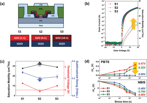
Table 1. Electrical parameters were obtained from the transfer curves of the PEALD IGZO/GZO TFTs (average values (± standard deviation) extracted from 10 devices for each condition).
Since only the top GZO layers of the IGZO/GZO stacks were modified, the chemical, physical, and optical properties of the GZO films were studied systematically. XPS analyses indicate the growth of high-quality GZO layers with negligible impurities, of which the atomic compositions are listed in Table . The metal cation ratios with respect to Ga: Zn subcycle ratio (nGa: nZn) are as follows: Ga0.37Zn0.63O (1:1), Ga0.69Zn0.31O (4:1), and Ga0.86Zn0.14O (10:1). Hereafter, each GZO film will be referred to as G1 (Ga0.37Zn0.63O), G2 (Ga0.69Zn0.31O), and G3 (Ga0.86Zn0.14O). The chemical bonding states of oxygen in the GZO films were examined by studying the O1s peaks of the XPS spectra, as shown in Figure (a). The O 1s peaks were calibrated with respect to 284.5 eV of the C–C bond and resolved into three subpeaks, representing the information occurring from the O-M bonds, oxygen-deficient sites, and OH groups, centered at 530.54 ± 0.03 eV, 531.91 ± 0.06 eV, and 532.87 ± 0.07 eV, respectively (Figure S4). The areal fractions of the oxygen deficiency and OH subpeaks arising from G1 are 18.6% and 4.6%, respectively, higher than those of G2 and G3. The optical bandgap of the GZO layers was extracted from UV-vis measurements, as depicted in Figure (b). The bandgap gradually increases with increasing Ga content, most likely owing to the contribution of GaOx generally known as a wide bandgap material (∼4.9 eV) [Citation24,Citation25]. Figures (c–d) indicate the differences in physical properties concerning the GZO composition. Figure (c) presents the XRD data, where a broad crystal peak arises from the G1 film that has a relatively high Zn content, while G2 and G3 appear to be amorphous. The AFM topography images in Figure (d) reflect the relatively high surface roughness of G1, which also suggests the presence of a crystalline phase. G2 and G3 exhibit smooth surfaces with average roughness values smaller than 0.3 nm. It may therefore be assumed that the defective GZO in G1, in conjunction with the surface roughness due to the partial crystallinity and the oxygen-related defects, induces a high density of electron traps once integrated into TFTs in the form of IGZO/GZO bilayers. The defects may be present at the IGZO/GZO interface or within the GZO bulk, which deteriorates the stability of the S1 devices. The subthreshold swing (S.S.) values in Table reflect the relatively high interface trap density in S1. In contrast, the properties of the G2 and G3 films are not significantly different according to the XPS, XRD, and AFM analyses. Thus, further characterization is necessary to elucidate the TFT performance and stability results of S2 and S3.
Figure 2. The chemical, optical, and physical properties of the PEALD GZO thin films (G1–G3): (a) XPS spectra of O 1 s; (b) optical band gap; (c) crystallinity; and (d) root mean square (RMS) roughness.
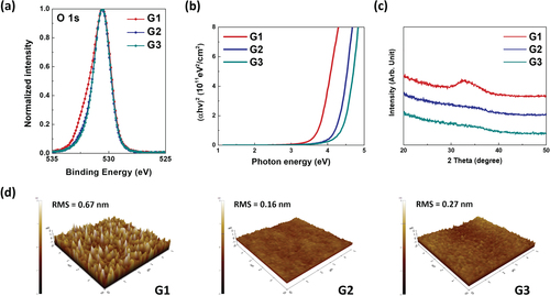
Table 2. Elemental compositions (Ga, Zn, and O were analyzed before surface etching) and carbon impurities (C was analyzed after surface etching) of PEALD GZO films obtained by XPS analyses with respect to Ga: Zn subcycle ratios.
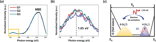
In addition to the above studies, PL analyses were conducted from the GZO films, and the results are detailed in Figure . The peak at approximately 3.10 eV in Figure (a) is related to near-band-edge (NBE) emission [Citation26,Citation27]. Deep-level PL emission is observed at a peak located near 1.65 eV. Figure (b) represents its magnification. Light emission in n-type oxide semiconductors is generally described as the result of the deexcitation of electrons in shallow subgap levels near the conduction band minimum (CBM) into levels of subgap states near the valence band maximum (VBM). In other words, 1.65 eV of energy is emitted as electrons are deexcited from shallow VO+ defect states into deep VO0 states [Citation28,Citation29]. The G2 film exhibits the lowest PL intensity, whereas G1 and G3 display similar intensities in Figure (b). The G2 film exhibits a relatively low PL emission intensity near 1.65 eV than G1 and G3, and it may thus be assumed that it contains fewer shallow-level defects near the conduction band. Figure (c) shows a simplified density of states (DOS) schematic based on the PL analysis, assuming that the bandgap values of all three GZO films are identical. One reason for the high performance and reliability of the corresponding S2 device may be interpreted to be due to the minimization of trap sites in the G2 film, which induces a high-quality IGZO/GZO interface. This indicates that appropriate control of film composition via ALD helps reduce the defect density in TFT active layers, thus, improving the device's properties.
Figure 3. (a) PL spectra of the GZO thin films (G1–G3) and (b) magnified portion (photon energy from 1.5 to 1.85 eV). (c) Schematic illustrating the deexcitation of electrons between subgap defect states.
The energy band alignment is also an essential factor that influences the electrical characteristics and reliability of TFTs that incorporate active stacks composed of different materials [Citation30]. Figure shows the band alignment in the IGZO/GZO bilayers based on the UV-vis and UPS analyses of the separate IGZO and GZO films (Figures (a) and S5). As the Ga content increases in the top GZO film of the active stacks (used for devices S1 to S3), the GZO bandgap widens while the Fermi level lowers further from the CBM. This increases the conduction band offset (CBO) difference concerning the IGZO region, from 0.46 eV to 1.14 eV. In the case of the valence band offset (VBO) differences, the largest value is observed in the active layer structure of the S2 device (0.68 eV), while those for the S1 and S3 TFTs are only 0.21 and 0.27 eV, respectively. From the CBO results and the fact that the individual GZO layers are not as conductive as IGZO (Figure S1), it may be anticipated that the main conduction channel forms on the IGZO side of the bilayer, with accumulated carriers near the IGZO/GZO interface. Thus, band alignment modulation by composition control significantly affects carrier movement and causes differences in the electrical performance and stability of the TFT.
Figure 4. Schematic band diagram of bilayer IGZO/GZO TFTs (S1-S3) with different GZO compositions. The Ga: Zn ALD subcycle ratios of the GZO films are (a) 1:1, (b) 4:1, and (c) 10:1.
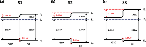
Figure consists of schematic diagrams describing the PBTS and NBIS degradation mechanisms of the S1–S3 devices based on the band alignment analyses. The main cause of PBTS instability is the trapping or injection of accumulated carriers by a positive gate bias [Citation31,Citation32]. Since identical GI layers were used in all devices, the difference in PBTS reliability may be attributed to the trapping of electrons at defective sites near the IGZO/GZO boundaries or GZO/GI interfaces. As illustrated in Figure (a), the main channel of the S1–S3 devices is formed on the IGZO side of the IGZO/GZO stack, and electrons accumulate at the IGZO/GZO interface due to the positive gate voltage bias. In the S1 device, the relatively small CBO difference may allow a portion of the free carrier to accumulate on the GZO/GI interface, thus forming a subchannel region. More electrons may thus be trapped in the defective G1 layer that contains a higher amount of VO-related defects than S2 and S3 TFTs. In addition, the roughness induced on the G1 surface owing to its partial crystallinity may also allow the trapping of electrons near the main IGZO/GZO interface, which accounts well for the poor stability under PBTS [Citation17]. The G3 layer in the S3 device exhibits a slightly higher surface roughness and VO defect content than the G2 layer of the S2 device, as deduced from the AFM and PL analyses. Therefore, one may anticipate a less defective IGZO/GZO interface in S2, which reflects well its considerably improved reliability. The findings imply that interface engineering is possible by thoroughly tailoring the composition of GZO films on top of IGZO using PEALD, which allows the physical separation of the main conductive channel from the gate insulator and reduces the number of defect sites in the vicinity of the IGZO/GZO interface. As such, the PBTS stability of the resulting device may be enhanced tremendously while preserving high field-effect mobility.
Figure 5. Degradation mechanism of IGZO/GZO TFTs (S1-S3) under (a) PBTS (60°C, 2 MV cm−1) and (b) NBIS (1000 lux, −2 MV cm−1).
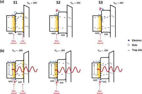
Figure (b) presents the behavior of the S1-S3 TFTs under NBIS. Several research groups have reported the degradation mechanisms of oxide TFTs under NBIS, such as photo-generated hole trapping or injection [Citation33], photoionization of oxygen vacancy defects [Citation34], and interactions with ambient conditions [Citation35]. We observed that all IGZO/GZO bilayer devices improve NBIS degradation by more than twice than that of the IGZO-based S0 TFT. In the presence of light, the deep-level VO0 states are photoexcited to the shallow VO2+ states, which generate excessive free carriers, resulting in significant NBIS degradation in a single IGZO device. By applying the IGZO/GZO stack structure, NBIS reliability may improve, owing to the reduction of the absolute number of VO-related defects in the active layer [Citation36]. Moreover, if one assumes that photogenerated hole carriers may move from the IGZO to the GI, the insertion of a GZO layer in between creates a VBO that acts as a hole barrier, which results in smaller amounts of holes being trapped at the active/GI interface. Yasuharu et al. suggested the possible presence of another type of hole trap in the GI [Citation37]. Their research proposed that InSi defects formed by the diffusion of indium from IGZO to the GI may act as hole trap sites and induce device degradation under NBIS (Figure S6b). The In-free GZO layers in the present work may also suppress the formation of InSi defects by suppressing the diffusion of indium to the GI region.
4. Conclusions
This study demonstrated that the appropriate composition control of indium-free GZO layers via PEALD in IGZO/GZO bilayer stacks is an effective method to improve the stability of oxide TFTs without compromising the electrical performance. Two major effects are suggested as a result of applying a GZO layer on top of IGZO: (1) interface engineering and (2) band alignment modulation. The optical, physical, and chemical properties of the GZO films could be optimized at a Ga:Zn ALD subcycle ratio of 4:1, which resulted in the least number of defects that can act as electron traps. The conductive channel is suspected to form mainly on the IGZO side of the IGZO/GZO stack, preserving a high field effect mobility. With an optimum GZO composition, the device reliability was also shown to improve, most likely as a result of reduced defect states near the IGZO/GZO interface and the physical separation of the main channel from the GI. Band alignment modulation induces conduction band and valence band offset differences between the IGZO and GZO semiconductors, which may suppress the diffusion of electrons or holes from the IGZO to the GI region under PBTS and NBIS, respectively. The resulting IGZO/GZO TFTs exhibited an average saturation mobility (µsat) of 31.9 cm2 V−1 s−1, an average threshold voltage (Vth) of −0.14 V, and an average subthreshold swing (SS) of 0.20 V/decade. The amount of Vth shift (ΔVth) under PBTS and NBIS was reduced by approximately 35.1% and 57.6%, respectively, compared to single-layered IGZO devices. Therefore, applying the IGZO/GZO bilayer active structures with meticulous control over the film quality may help improve device reliability without significantly compromising their electrical performance.
Supplemental Material
Download MS Word (493.6 KB)Disclosure statement
No potential conflict of interest was reported by the author(s).
Additional information
Funding
Notes on contributors

Hye-Jin Oh
Hye-Jin Oh received a B.S. degree from the Division of Materials Science and Engineering, Kookmin University, Seoul, South Korea. She has been researching thin-film transistors based on metal oxide materials.

Yoon-Seo Kim
Yoon-Seo Kim received a B.S. degree from the Division of Materials Science and Engineering, at Hanyang University, Seoul, South Korea. He has been researching thin-film transistors based on metal oxide materials.

Hyun-Jun Jeong
Hyun-Jun Jeong received his Ph.D. degree in Material Science and Engineering from Hanyang University, South Korea in 2020. He is currently working at Samsung Display Co., Ltd. He received the 2015 KIDS Bronze Award presented by the International Meeting on Information Display (IMID), South Korea.

Sunhee Lee
Sunhee Lee received his Ph.D. degree from the Department of Electrical Engineering at Purdue University in 2011 and then worked at Samsung Advanced Institute of Technology until 2013. Since 2013, he has been at Samsung Display Co., Ltd., developing oxide semiconductor-based backplane technology.

Joon Seok Park
Joon Seok Park received his Ph.D. degree in Materials Science and Engineering from Stanford University in 2008. He was part of the research staff at the Samsung Advanced Institute of Technology from 2008 to 2013, where he researched oxide semiconductor TFTs. After joining Samsung Display Co., Ltd. in 2013, he has committed himself to the development of oxide TFT backplanes for OLED applications.

Jin-Seong Park
Jin-Seong Park received a Ph.D. degree from the Department of Materials Science and Engineering, KAIST, Daejeon, South Korea, in 2002 and then worked at Roy Gordon’s Laboratory in Harvard, USA, as a postdoctoral associate. Since 2013, he has been a professor at the Division of Materials Science and Engineering at Hanyang University, Seoul, South Korea. He has received the Merck Young Scientist Award (2014), and the Merck Special Award in ALD Materials and Process (2021).
References
- K. Nomura, H. Ohta, A. Takagi, T. Kamiya, M. Hirano, and H. Hosono, Nature 432 (7016), 488–492 (2004).
- K. Nomura, A. Takagi, T. Kamiya, H. Ohta, M. Hirano, H. Hosono, and J.J. Appl, J. Appl. Physics, Part 1 Regul. Pap. Short Notes Rev. 45 (5B), 4303–4308 (2006).
- M. Nag, A. Chasin, M. Rockele, S. Steudel, K. Myny, A. Bhoolokam, A. Tripathi, B. Van Der Putten, A. Kumar, J.L. Van Der Steen, J. Genoe, F. Li, J. Maas, E. Van Veenendaal, G. Gelinck, and P. Heremans, J. Soc. Inf. Disp. 21 (3), 129–136 (2013).
- E. Yamamoto, S. Saito, K. Sato, K. Furutani, Y. Yakubo, T. Onuki, T. Matsuzaki, T. Atsumi, Y. Ando, T. Murakawa, K. Kato, and S. Yamazaki, ECS Trans. 90 (1), 139–146 (2019).
- Q. Hu, C. Gu, Q. Li, S. Zhu, S. Liu, Y. Li, L. Zhang, R. Huang, and Y. Wu, Adv. Mater. 35, 2210554 (2023).
- H. Han, S. Jang, D. Kim, T. Kim, H. Cho, H. Shin, and C. Choi, Electronics 11 (1), 53 (2021).
- F. Mo, T. Saraya, T. Hiramoto, and M. Kobayashi, Appl. Phys. Express 13 (7), 074005 (2020).
- T. Nakagawa, Y. Negoro, S. Yoneda, H. Shishido, H. Kobayashi, M. Oota, T. Kawata, T. Ikeda, and S. Yamazaki, Jpn. J. Appl. Phys. 59 (11), 110904 (2020).
- S. Jeon, S. Park, I. Song, J.H. Hur, J. Park, H. Kim, S. Kim, S. Kim, H. Yin, U.I. Chung, E. Lee, and C. Kim, ACS Appl. Mater. Interfaces 3 (1), 1–6 (2011).
- Y.S. Rim, H. Chen, X. Kou, H.S. Duan, H. Zhou, M. Cai, H.J. Kim, and Y. Yang, Adv. Mater. 26 (25), 4273–4278 (2014).
- Y.J. Chung, U.K. Kim, E.S. Hwang, and C.S. Hwang, Appl. Phys. Lett. 105 (1), 013508 (2014).
- K. Liang, Y. Wang, S. Shao, M. Luo, V. Pecunia, L. Shao, J. Zhao, Z. Chen, L. Mo, and Z. Cui, J. Mater. Chem. C 7, 6169 (2019).
- A. Abliz, J. Wang, L. Xu, D. Wan, L. Liao, C. Ye, C. Liu, C. Jiang, H. Chen, and T. Guo, Appl. Phys. Lett. 108 (21), 213501 (2016).
- H. Xu, M. Xu, Z. Chen, M. Li, J. Zou, H. Tao, L. Wang, and J. Peng, IEEE Electron Device Lett. 37 (1), 57–59 (2016).
- J. He, G. Li, Y. Lv, C. Wang, C. Liu, J. Li, D. Flandre, H. Chen, T. Guo, and L. Liao, Adv. Electron. Mater. 5, 1 (2019).
- M.M. Billah, A.B. Siddik, J.B. Kim, D.K. Yim, S.Y. Choi, J. Liu, D. Severin, M. Hanika, M. Bender, and J. Jang, Adv. Electron. Mater. 7 (3), 1 (2021).
- Y.S. Kim, W.B. Lee, H.J. Oh, T.H. Hong, and J.S. Park, Adv. Mater. Interfaces 9, 1 (2022).
- S. Zastrow, J. Gooth, T. Boehnert, S. Heiderich, W. Toellner, S. Heimann, S. Schulz, and K. Nielsch, Semicond. Sci. Technol. 28 (3), 035010 (2013).
- A. Wang, T. Chen, S. Lu, Z. Wu, Y. Li, H. Chen, and Y. Wang, Nanoscale Res. Lett. 10, 1–10 (2015).
- J. Sheng, T.H. Hong, H.M. Lee, K.R. Kim, M. Sasase, J. Kim, H. Hosono, and J.S. Park, ACS Appl. Mater. Interfaces 11 (43), 40300–40309 (2019).
- M.H. Cho, C.H. Choi, H.J. Seul, H.C. Cho, and J.K. Jeong, ACS Appl. Mater. Interfaces 13 (14), 16628–16640 (2021).
- R.L. Weiher, and R.P. Ley, J. Appl. Phys. 37 (1), 299–302 (1966).
- R.L. Weiher, J. Appl. Phys. 33 (9), 2834–2839 (1962).
- C.I. Bright, Opt. Thin Film. Coatings From Mater. to Appl 4166, 741–788 (2018).
- J. Kim, T. Sekiya, N. Miyokawa, N. Watanabe, K. Kimoto, K. Ide, Y. Toda, S. Ueda, N. Ohashi, H. Hiramatsu, H. Hosono, and T. Kamiya, NPG Asia Mater. 9 (3), e359 (2017).
- J. Zhang, X. Wen, L. Hu, W. Xu, D. Zhu, P. Cao, W. Liu, S. Han, X. Liu, F. Jia, Y. Zeng, and Y. Lu, J. Mater. Chem. C 5, 2388 (2017).
- A. Rajan, H.K. Yadav, V. Gupta, and M. Tomar, Procedia Eng. 94, 44–51 (2014).
- E.K.H. Yu, P.C. Lai, and J. Kanicki, IEEE Trans. Electron Devices 65 (3), 1258–1261 (2018).
- W.S. Liu, Y.H. Lin, C.L. Huang, and C.W. Wang, IEEE Trans. Electron Devices 64 (6), 2533–2541 (2017).
- Y.Y. Zhang, L.X. Qian, W.B. Ge, P.T. Lai, and X.Z. Liu, Phys. Status Solidi Appl. Mater. Sci. 215, 1 (2018).
- R.B.M. Cross, and M.M. De Souza, Appl. Phys. Lett. 89, 28 (2006).
- Z. Zhu, W. Cao, X. Huang, Z. Shi, D. Zhou, and W. Xu, Micromachines 13, 1 (2022).
- K.H. Ji, J.I. Kim, H.Y. Jung, S.Y. Park, R. Choi, Y.G. Mo, and J.K. Jeong, Microelectronic Eng. 88 (7), 1412–1416 (2011).
- J. Zhang, P. Dong, K. Dang, Y. Zhang, Q. Yan, H. Xiang, J. Su, Z. Liu, M. Si, J. Gao, M. Kong, H. Zhou, and Y. Hao, Nat. Commun 13, 1 (2022).
- J.K. Jeong, J. Mater. Res. 28 (16), 2071–2084 (2013).
- M. Mativenga, J.G. Um, and J. Jang, Appl. Sci. 7 (9), 885 (2017).
- Y. Hosaka, T. Obonai, M. Dobashi, T. Nakayama, Y. Shima, M. Ohno, and S. Yamazaki, Dig. Tech. Pap. - SID Int. Symp. 53 (1), 1066–1069 (2022).