
ABSTRACT
We report a new methodology to synthesize thin films with exceptional microstructural control via systematic, in-situ seeding of nanocrystals into amorphous precursor films. When the amorphous films are subsequently crystallized by thermal annealing, the nanocrystals serve as preferential grain nucleation sites and control their micro/nanostructure. We demonstrate the capability of this methodology by precisely tailoring the size, geometry and spatial distribution of nanostructured grains in structural (TiAl) as well as functional (TiNi) thin films. This synthesis methodology is likely to be applicable to other amorphously grown materials and enables explicit microstructural control in a wide spectrum of thin films/coatings.
IMPACT STATEMENT
This paper describes a novel synthesis methodology to precisely tailor the microstructure of thin films and reveals the mechanisms underlying this methodology using in-situ TEM annealing experiments.
GRAPHICAL ABSTRACT
1. Introduction
Nanostructured thin films/coatings have widespread applications in thermal barrier systems, cutting tools, biomedical implants, microelectromechanical systems, and integrated circuits. In all these applications, the mechanical properties of the films/coatings, which are intrinsically related to their microstructure, are of paramount importance. Therefore, the ability to robustly control the microstructure (mean size, orientation, size dispersion and spatial distribution of grains) of nanostructured films/coatings would enable us to optimize their mechanical properties and enhance their performance. Physical vapor deposition (PVD) processes, which are most commonly used to synthesize high quality nanostructured thin films, allow us to vary the texture [Citation1] and mean grain size [Citation2] by changing the film thickness, substrate, deposition rate or temperature [Citation3]. Nevertheless, in PVD-synthesized films it is difficult to decouple the mean grain size and thickness and there is little control over grain size dispersion or spatial distribution.
Hence, researchers have experimented with different methods to alter the various stages of microstructural evolution in thin films, which in the case of Volmer-Weber growth includes nucleation, island formation, coalescence and grain coarsening [Citation4]. In particular, several studies have focused on controlling the grain nucleation process through the use of seed layers or isolated seed crystals. The seed layers/crystals have been found to alter the nucleation kinetics [Citation5], enhance epitaxial growth [Citation6], and aid the growth of highly oriented polycrystalline films [Citation7]. However, these techniques have only been used to control a narrow set of microstructural parameters in specific materials and their wider applicability is unclear. In essence, a synthesis methodology that can be used to systematically and independently tune a broad set of microstructural variables in thin film materials is still lacking.
Here, we report a new methodology to synthesize thin films with exceptional microstructural control from amorphous precursor films. By systematic, in-situ deposition of seed layers, we first create a dispersion of crystalline nanoscale domains (seeds) in the amorphously grown films. We then exploit the ability of these seeds to preferentially nucleate grains during thermal annealing to rigorously control the final micro/nanostructure of the films. We demonstrate the capability and generality of this approach by tailoring the mean size, geometry and spatial distribution of grains in structural (TiAl) as well as functional (TiNi) thin films. This approach could potentially be applied to other amorphously grown materials and enables the synthesis of thin films/coatings with tailored microstructures for a wide spectrum of applications.
2. Experimental details
2.1. Film deposition and characterization
200 µm-thick Si (100) wafers with a 60 nm thick SiNx diffusion barrier layer (grown by plasma enhanced chemical vapor deposition) on top were used as substrates for all depositions. Amorphous TiAl and TiNi films were co-deposited on the substrate (rotated to ensure uniformity in film thickness and composition) by DC magnetron sputtering at room temperature (RT) at a base pressure of ∼5 × 10⁻⁸ Torr and argon pressure of 3 mTorr. 99.999% pure Ti, Al and Ni targets were used for deposition and film composition was controlled by tuning the power of individual sputtering guns.
The co-deposition of the amorphous TiAl/TiNi layers was stopped periodically and thin seed layers (0.5–2 nm thickness) of pure Ti or Al were deposited on them. After seed layer deposition, the co-deposition of TiAl/TiNi was resumed so that the seed layer was encapsulated by amorphous layers. This process was repeated to obtain films comprised of single/multiple seed layers and desired thickness. The deposition rates for the amorphous TiAl/TiNi layers and seed layers were 10–15 nm/min and 5–8 nm/min, respectively, for all films.
After the deposition was complete, the films were crystallized by annealing in vacuum (<10−6 Torr) either in the sputtering chamber or in a FEI Tecnai F20 transmission electron microscope (TEM). For annealing experiments inside the sputtering chamber, the temperature was increased to the final value within a few minutes and held steady for the desired amount of time. For in-situ TEM annealing, the temperature was increased gradually to counteract the thermal drift of the specimen. The microstructures of the synthesized films were characterized by TEM and X-ray diffraction (XRD), whereas Rutherford backscattering spectrometry was used to determine the composition. All the grain sizes reported in the manuscript correspond to measurements from TEM bright-field/dark-field images. More details on TEM specimen preparation are provided in the supplementary information document.
2.2. Synthesis methodology
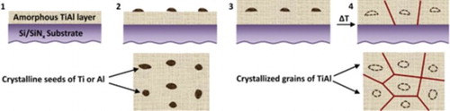
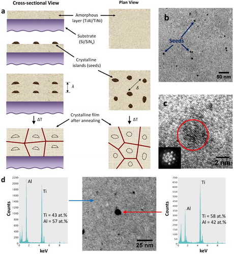
The first step of the synthesis process (Figure (a)) is the co-deposition of a relatively thick, amorphous layer (20–500 nm) of the material at RT. The next step is the deposition of a seed layer (0.5–2 nm thick) that has a crystalline structure at RT. As this layer is very thin, it is non-contiguous and results in the formation of isolated crystalline seeds. A second amorphous layer is then deposited to sandwich the seeds. These steps are repeated until the desired overall film thickness is obtained. λ is the spacing between seed layers along the film thickness. The average in-plane spacing (δ) between the seeds can be controlled by varying the seed layer thickness, deposition rate and temperature [Citation3]. Finally, the amorphous matrix with the seeds is crystallized by annealing at high temperature in vacuum. The seeds serve as preferential grain nucleation sites during annealing and hence the grain heights and diameters scale with λ and δ, respectively. Since both λ and δ can be independently varied during each step of the growth process, the size, dispersion and spatial distribution of grains can be explicitly controlled.
Figure 1. (a) Schematic of the synthesis process. (b) TEM bright-field image showing crystalline Ti seeds on an amorphous TiAl layer. (c) HR-TEM image showing the atoms on the (0001) plane of a Ti seed (red circle) surrounded by the amorphous TiAl matrix. The CBED pattern of the seed is shown in the inset. (d) TEM bright-field image of an as-deposited 40 nm amorphous TiAl film with a 1 nm Ti seed layer in the middle. EDS analysis of the seed region (right, red arrow) and the amorphous matrix (left, blue arrow) reveals the difference in their composition. Note that the composition of the seed region includes the amorphous matrix encapsulating the seed.
3. Results
We performed a series of systematic experiments to uncover the effects of seed density and distribution on the microstructure of the crystallized films. The amorphous layers in the TiAl films were chosen to have a nominal atomic composition of 45% Ti and 55% Al, whereas the TiNi films were equiatomic. Since the seed crystals play a key role in controlling the crystallization process, we first verified that the deposition of seed layers leads to the formation of well-dispersed seeds (Figure (b)). We confirmed the crystallinity of the seeds (Figure (c)) using high resolution TEM (HR-TEM) and convergent beam electron diffraction (CBED) and verified their chemical composition (Figure (d)) using energy dispersive X-ray spectroscopy (EDS). It should be noted that the presence of well delineated seeds does not preclude the possibility of locally contiguous layers. Similarly, only a fraction of the seeds, which are sufficiently large and appropriately oriented to produce diffraction contrast, are visible in the bright-field TEM image. Nonetheless, we verified that the average size and spatial distribution of the seeds were significantly different for different seed layer thicknesses (Supplementary Figure 1), which strongly suggests that seed formation is not controlled by defects on the surface of the amorphous layer.
3.1. Effect of seed crystals on crystallization kinetics and grain size
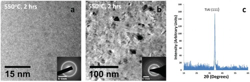
We found that the seeds modify both the crystallization temperature and the final microstructure of the films. When unseeded and seeded amorphous TiAl films were annealed at 550°C for a period of two hours, the unseeded film remained completely amorphous (Figure (a)). In contrast, the seeded film showed clear evidence of crystallization as revealed by TEM and XRD analysis (Figure (b,c)). In effect, the seeds reduced the temperature required for crystallization and accelerated the crystallization process.
Figure 2. TEM bright-field image of a TiAl film with no seed layer after 2 h of annealing at 550°C. This film remained completely amorphous as indicated by the diffuse ring in the selected area diffraction (SAD) pattern (inset). (b) TEM bright-field image of a TiAl film with a single 1 nm Ti seed layer in the middle after 2 h of annealing at 550°C. The film showed partial crystallization and spots started to appear in the SAD pattern (inset). (c) XRD pattern of the film in (b). The presence of a well-defined gamma-TiAl (111) peak indicates that the film has started to crystallize.
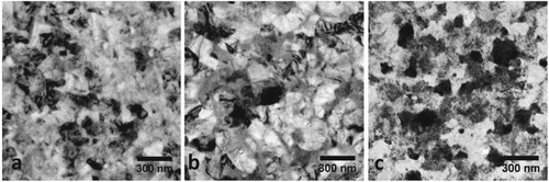
Interestingly, the seeded films also exhibited a much smaller mean grain size (dm) compared to the unseeded films when the annealing temperature was increased. Figure (a,b) show microstructures of TiAl films without and with Ti seeds annealed at 600°C for four hours. The unseeded film had dm = 1.15 ± 0.2 µm after annealing, whereas the seeded film had dm = 65 ± 35 nm. Notably, the seeded film retained its nanostructure (Figure (c)) even upon annealing at 750°C, which is approximately 0.6 times the melting temperature of TiAl. The same microstructural stability was also seen when an Al seed layer was used (Supplementary Figure 2).
Figure 3. Post-annealing bright-field TEM images of: (a) TiAl film with no seed layer (dm = 1.15 ± 0.2 µm). (b) TiAl film with a single 1 nm Ti seed layer (dm = 65 ± 35 nm). (c) TiAl film with a single 1 nm Ti seed layer (dm = 67 ± 39 nm). (d) TiNi film with no seed layer (dm = 1.44 ± 0.29 µm). (e) TiNi film with a single 1 nm Ti seed layer (dm = 540 ± 150 nm). (f) TiNi film with a single 1 nm Ti (dm = 580 ± 124 nm). All the films were 100 nm thick and the annealing temperature and time are indicated in the images. For all seeded films, the seed layer was deposited in the middle. The ± values in dm correspond to the standard deviation.
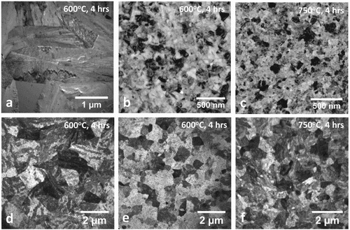
Note that the seed layers change the overall composition of Ti and Al in the film by less than 1% and do not induce the formation of additional phases, which may alter the grain size. Both unseeded and seeded films are composed only of the gamma phase (Supplementary Figure 3). The same trends in dm were observed in unseeded and seeded TiNi films (Figure (d–f)) but dm was higher compared to TiAl films. Similar to TiAl, only a single phase (martensite) could be identified in the TiNi films at RT.
3.2. Control of mean size, aspect ratio and spatial distribution of grains
As indicated in Figure , if the seeds act as preferential nucleation sites the average grain diameter and height should scale with δ and λ, respectively. To test this assumption, we systematically varied δ and λ and analyzed the resultant microstructures. To increase δ for a given seed layer thickness, we induced the seeds to coarsen and coalesce [Citation8] by increasing the temperature (Tseed) for a short period of time immediately after the seed layer was deposited. We note that Tseed was sufficiently small (≤150°C) to avoid crystallization of the amorphous layer underneath. After this step, the film was allowed to cool back to RT and the subsequent amorphous layer was deposited. Figure provides direct evidence that by altering δ, dm can be systematically varied. dm of the TiAl films was least when no seed coalescence was induced and progressively increased with increasing Tseed, even though all other deposition parameters, and annealing conditions for crystallization were identical.
Figure 4. TEM bright-field images of three different 100 nm thick TiAl films with a single 1 nm Ti seed layer (deposited in the middle) after annealing at 600°C for 4 h. In addition to the final 600°C annealing, the films in (b) and (c) were subjected to a 10 min anneal at 100°C and 150°C, respectively, immediately after seed layer deposition. The mean grain sizes are 65 ± 35 nm, 141 ± 50 nm and 176 ± 65 nm for the films in (a), (b) and (c), respectively.
To ascertain the effect of λ, we synthesized films with different number of seed layers and analyzed their microstructures through cross-sectional TEM (Figure ). When a single seed layer was used, the grains in the crystallized film were columnar and typically traversed the entire thickness (Figure (a,d)). In contrast, when multiple seed layers were used, multiple grains with a more equiaxed structure were observed (Figure (b,e)).
Figure 5. Cross-sectional TEM bright-field images of: (a) TiAl film with a single 1 nm Ti seed layer in the middle. (b) TiAl film with four equally spaced 1 nm Ti seed layers. (c) TiAl film with smaller seed layer spacing near the top and bottom and larger spacing in the middle. A gradient microstructure was formed upon annealing. (d) TiNi film with a single 1 nm Ti seed layer in the middle. (e) TiNi film with four equally spaced 1 nm Ti seed layers. (f) TiNi film with multiple seed layers and varying λ. A gradient microstructure was formed after annealing, similar to (c). All the films were annealed at 650°C for 4 h. The red arrows indicate the TiAl and TiNi film cross-sections.
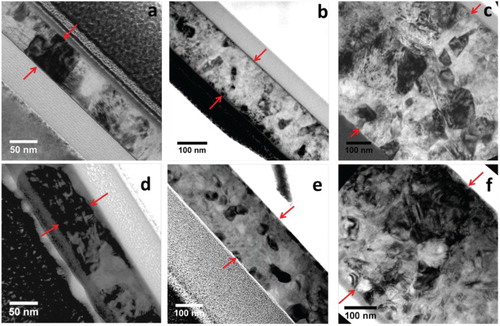
Apart from tailoring the grain diameters and geometry, the method also enables us to systematically control the size dispersion and spatial distribution of grains by varying λ and δ across the thickness. Figure (c,f) show films with gradient microstructures, composed of smaller grains near the top and bottom and larger grains in the middle, synthesized using this method. Supplementary Figure 4 shows another film with ultrafine grains in one half and nanocrystalline grains in the other half. Such heterogeneous microstructures can enable high strength and ductility [Citation9] and enhance recovery of inelastic strain during/after unloading [Citation10,Citation11].
3.3. In-situ TEM annealing experiments
To obtain further insights on how the seeds influence the crystallization process, we carried out in-situ TEM annealing of seeded and unseeded TiAl films. The experiments revealed that crystallization starts around 550°C in the seeded film with the simultaneous nucleation of a large number of grains (Figure (a)). At this temperature the grains were relatively small, with sizes ranging from 5 to 25 nm. When the temperature was increased to 650°C, limited grain coalescence occurred and the mean grain size increased to about 100 nm (Figure (b)). Further increase in temperature (up to 800°C), did not cause notable coarsening of the microstructure.
Figure 6. (a–b) TEM images from in-situ annealing of a 100 nm thick TiAl film with a single 1 nm Ti seed layer. (a) shows the film after heating at 550°C for 1 h, whereas (b) corresponds to the film after heating at 650°C for a further 30 min. (c–d) TEM images from in-situ annealing of an unseeded 100 nm thick TiAl film. (c) corresponds to 600°C annealing for 1 h and shows the nucleation of a large crystalline phase (red arrow), as revealed by the SAD pattern. The rest of the film (blue arrow) was still amorphous. (d) corresponds to further annealing at 650°C for 30 min and shows the formation of µm-sized grains.
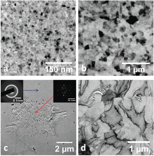
In contrast, the crystallization process was markedly different in the unseeded TiAl film. The film showed no crystallization at 550°C but a few crystalline islands nucleated upon increasing the temperature to 600°C. Typically, the islands were µm-sized (Figure (c)) and the spacing between the islands was also in micrometers. This resulted in a significantly larger mean grain size (Figure (d)) when the film was fully crystallized at 650°C. In other words, the crystallization of the unseeded amorphous TiAl films was growth controlled and not nucleation controlled, which has been observed in other amorphous alloy films as well [Citation12].
4. Discussion
The results described above unambiguously show that in-situ seeding of nanocrystals can be used to control the crystallization of amorphous films. The crystallization process is driven by the lower free energy of the crystalline structure compared to the amorphous one. While the crystalline phase is thermodynamically favored, there is an activation barrier for its nucleation and an increase in temperature is required to overcome this barrier and induce the amorphous to crystalline transformation [Citation13]. The seed crystals lower the activation barrier for nucleation and, thus, reduce the temperature needed for crystallization. Conversely, for a given crystallization temperature, the nucleation rate is much higher in a seeded film compared to an unseeded film, which leads to faster crystallization of the seeded film. In this respect, the seed crystals in our amorphous films play a role similar to that of grain refiners during the casting/solidification of metallic alloys [Citation14,Citation15]. During solidification, grain refiners act as substrates for the nucleation of the solid phase and lower the activation barrier, and hence the undercooling required, for the liquid to solid transformation.
The presence of numerous, closely spaced seed crystals leads to the simultaneous nucleation of a large number of grains whose average size when they impinge on each other is quite small (Figure (a)). While the small size at impingement is expected, there was limited grain growth in the TiAl films even at higher temperatures (Figure (c)). There are two possible reasons for this microstructural stability. Firstly, because these films have a single seed layer, the nucleated grains traverse the entire thickness of the film and develop a 2 D columnar structure. Once a columnar structure forms, the average grain boundary energy per unit volume (EGB) reduces, and since the rate of increase in average grain diameter is directly proportional to EGB, grain growth slows down [Citation8]. In addition, the formation of thermal grooves on the surface lowers grain boundary mobility, resulting in the stagnation of normal grain growth [Citation16]. Once normal grain growth stops, further increase in average grain size usually occurs through abnormal (secondary) grain growth. In abnormal grain growth, which is driven by surface energy minimization, a subpopulation of grains with orientations that lead to lower surface energies grow at the expense of other grains [Citation17]. However, the seeded TiAl films have a strong (111) texture (Figure (c), Supplementary Figure 3(a)), i.e. most of the grains have a low surface energy [Citation18], and hence abnormal grain growth is also restricted. Note that the unseeded films also have single grains traversing the thickness and a (111) texture (Supplementary Figure 3(b)). However, the crystalline islands in those films are µm-sized (Figure (c)) even before impingement and hence their final grain size is much larger.
We also checked if the potential formation of a thin oxide scale when the amorphous layer deposition is interrupted (to deposit the seed layer) could be responsible for the microstructural stability of the seeded films. To do so, we synthesized two 100 nm thick TiAl films, both without a seed layer. For the first film, we deposited a 50 nm thick amorphous layer, interrupted the deposition for 2 min (time typically needed for seed layer deposition) and then deposited another 50 nm layer. The second film was deposited without interruption. When we annealed both these unseeded films at 600°C for 4 h in vacuum, their mean grain sizes after crystallization was nearly identical (∼ 1 µm) and much larger than the seeded films. This confirms that the limited grain growth in the seeded films cannot be explained by oxide scale formation during deposition.
As noted in the introduction, the primary objective of this work was to establish a new methodology to independently control a broad range of microstructural parameters in thin films. To validate the methodology, we specifically chose two binary alloys—TiAl, a structural material [Citation19] and TiNi, a functional material which is widely used as thin film actuators in micromechanical systems [Citation20]—for the following reasons. First, both TiAl [Citation21] and TiNi [Citation22] can be easily deposited in the amorphous state at RT, which is essential for the methodology to work. More importantly, binary alloys have a greater tendency to spontaneously crystallize compared to alloys with more constituent elements (most bulk metallic glasses have 3 or more constituent elements for this reason). Hence, seed-mediated, controlled grain nucleation is more likely to be disrupted by spontaneous crystallization in binary alloys. Therefore, if the methodology is robust enough for binary alloys, it will likely apply to more complex alloys as well. In addition, by choosing TiAl and TiNi, we could verify that the methodology works for materials with different crystal structures (face centered tetragonal for gamma TiAl and body centered cubic/monoclinic for TiNi).
In this context, it is worth noting that materials synthesized by vapor deposition are farther from equilibrium compared to those obtained by liquid-to-solid processes typically used to produce bulk metallic glasses. Thus, a wide spectrum of metallic alloys [Citation23] and ceramics [Citation24,Citation25] can be deposited as amorphous films using a variety of PVD processes. Given that seed layers have been shown to influence the growth of ceramic nanostructures [Citation26] as well, it is reasonable to expect that the methodology can be applied to a broad class of amorphously deposited materials.
5. Conclusions
In this study, we have outlined a new methodology to explicitly control the microstructure of thin films and demonstrated its viability by tailoring the size, geometry and size/spatial distribution of grains in TiAl and TiNi films deposited by magnetron sputtering. The method is likely to be applicable to other amorphously grown materials as well as other PVD processes such as thermal or electron beam evaporation. By choosing the appropriate seed layers and deposition conditions, this approach can enable the synthesis of novel thin film materials with unique microstructural features and physical properties.
MRL_SI_Rev.pdf
Download PDF (710.7 KB)Acknowledgements
We gratefully acknowledge the use of facilities at the John M. Cowley Centre for High Resolution Electron Microscopy and at the Centre for Solid State Electronics Research at Arizona State University.
Disclosure statement
Arizona State University has applied for a patent (application no. PCT/US15/59162) related to the synthesis methodology and materials produced in this work.
ORCID
Jagannathan Rajagopalan http://orcid.org/0000-0002-0146-0805
Additional information
Funding
Related Research Data
References
- Izadi E, Rajagopalan J. Texture dependent strain rate sensitivity of ultrafine-grained aluminum films. Scr Mater. 2016;114:65–69. doi: 10.1016/j.scriptamat.2015.12.003
- Vopsaroiu M, Fernandez GV, Thwaites MJ, et al. Deposition of polycrystalline thin films with controlled grain size. J Phys D Appl Phys. 2005;38:490–496. doi: 10.1088/0022-3727/38/3/022
- Thompson CV. Structure evolution during processing of polycrystalline films. Annu Rev Mater Sci. 2000;30:159–190. doi: 10.1146/annurev.matsci.30.1.159
- Petrov I, Barna PB, Hultman L, et al. Microstructural evolution during film growth. J Vac Sci Technol A Vac Surf Films. 2003;21:S117. doi: 10.1116/1.1601610
- Buijnsters JG, Celis J-P, Hendrikx RWA, et al. Metallic seed nanolayers for enhanced nucleation of nanocrystalline diamond thin films. J Phys Chem C. 2013;117:23322–23332. doi: 10.1021/jp4071482
- Harp GR, Parkin SSP. Seeded epitaxy of metals by sputter deposition. Appl Phys Lett. 1994;65:3063–3065. doi: 10.1063/1.112507
- Miller KT, Lange FF. Highly oriented thin films of cubic zirconia on sapphire through grain growth seeding. JMater Res. 1991;6:2387–2392. doi: 10.1557/JMR.1991.2387
- Thompson CV. Grain growth in thin films. Annu Rev Mater Sci. 1990;20:245–268. doi: 10.1146/annurev.ms.20.080190.001333
- Wu X, Jiang P, Chen L, et al. Extraordinary strain hardening by gradient structure. PNAS. 2014;111:7197–7201. doi: 10.1073/pnas.1324069111
- Rajagopalan J, Han JH, Saif MTA. Bauschinger effect in unpassivated freestanding nanoscale metal films. Scr Mater. 2008;59:734–737. doi: 10.1016/j.scriptamat.2008.06.010
- Rajagopalan J, Han JH, Saif MTA. Plastic deformation recovery in freestanding nanocrystalline aluminum and gold thin films. Science. 2007;315:1831–1834. doi: 10.1126/science.1137580
- Lee D, Zhao B, Perim E, et al. Crystallization behavior upon heating and cooling in Cu 50 Zr 50 metallic glass thin films. Acta Mater. 2016;121:68–77. doi: 10.1016/j.actamat.2016.08.076
- Greer AL. Crystallization of amorphous alloys. Metall Mater Trans A. 1996;27:549–555. doi: 10.1007/BF02648945
- Easton M, StJohn D. Grain refinement of aluminum alloys: part I. The nucleant and solute paradigms—a review of the literature. Metall Mater Trans A. 1999;30:1613–1623. doi: 10.1007/s11661-999-0098-5
- Easton M, StJohn D. Grain refinement of aluminum alloys: part II. Confirmation of, and a mechanism for, the solute paradigm. Metall Mater Trans A. 1999;30:1625–1633. doi: 10.1007/s11661-999-0099-4
- Mullins WW. The effect of thermal grooving on grain boundary motion. Acta Metall. 1958;6:414–427. doi: 10.1016/0001-6160(58)90020-8
- Wong CC, Smith HI, Thompson CV. Surface-energy-driven secondary grain growth in thin Au films. Appl Phys Lett. 1986;48:335–337. doi: 10.1063/1.96543
- Vitos L, Ruban AV, Skriver HL, et al. The surface energy of metals. Surf Sci. 1998;411:186–202. doi: 10.1016/S0039-6028(98)00363-X
- Yamaguchi M, Inui H, Ito K. High-temperature structural intermetallics. Acta Mater. 2000;48:307–322. doi: 10.1016/S1359-6454(99)00301-8
- Fu Y, Du H, Huang W, et al. TiNi-based thin films in MEMS applications: a review. Sens Actuators A Phys. 2004;112:395–408. doi: 10.1016/j.sna.2004.02.019
- Sarkar R, Ebner C, Izadi E, et al. Revealing anelasticity and structural rearrangements in nanoscale metallic glass films using in situ TEM diffraction. Mater Res Lett. 2017;5:135–143.
- Chu JP, Lai YW, Lin TN, et al. Deposition and characterization of TiNi-base thin films by sputtering. Mat Sci Eng A. 2000;277:11–17. doi: 10.1016/S0921-5093(99)00560-2
- Chu JP, Jang JSC, Huang JC, et al. Thin film metallic glasses: unique properties and potential applications. Thin Solid Films. 2012;520:5097–5122. doi: 10.1016/j.tsf.2012.03.092
- El Khakani MAE, Chaker M, Jean A, et al. Hardness and Young’s modulus of amorphous a-SiC thin films determined by nanoindentation and bulge tests. J Mater Res. 1994;9:96–103. doi: 10.1557/JMR.1994.0096
- Rincón C, Romero J, Esteve J, et al. Effects of carbon incorporation in tungsten carbide films deposited by r.f. magnetron sputtering: single layers and multilayers. Surf Coat Technol. 2003;163-164:386–391. doi: 10.1016/S0257-8972(02)00635-7
- Greene LE, Law M, Tan DH, et al. General route to vertical ZnO nanowire arrays using textured ZnO seeds. Nano Lett. 2005;5:1231–1236. doi: 10.1021/nl050788p