2,181
Views
8
CrossRef citations to date
0
Altmetric
Report

Surface strengthening of single-crystal alumina by high-temperature laser shock peening

, , , , &
Pages 155-161 | Received 01 Aug 2020, Published online: 23 Dec 2020

Abstract

This manuscript reports a novel process of high-temperature laser shock peening (HTLSP) for surface strengthening of single-crystal ceramics such as sapphire and reveals its fundamental mechanisms. HTLSP at 1200°C can induce a high compressive residual stress on the surface of sapphire while minimize the damage of laser-driven shock waves. Transmission electron microscopy characterizations revealed high dislocation densities near the surface, suggesting that plastic deformation at an ultrahigh strain rate was generated by the high shock wave pressure. The HTLSP-induced compressive residual stress can significantly improve the hardness and fracture toughness of sapphire, while maintain its outstanding optical transmittance.
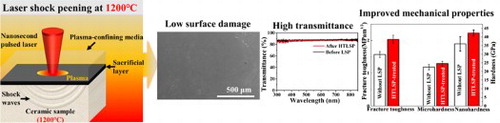
GRAPHICAL ABSTRACT

IMPACT STATEMENT

This manuscript reports a novel process of high-temperature laser shock peening for surface strengthening of single-crystal ceramics, and reveals mechanisms related to the interactions between laser-driven shock waves and ceramics.

This article is part of the following collections:
Modelling and Simulations

1. Introduction

Single-crystal alumina (sapphire) is an outstanding structural and optical ceramic material that has a wide range of critical applications because of its excellent light transmission, chemical resistance, superior mechanical performance, and high thermal stability. However, its low fracture toughness (<2 MPa•m1/2) results in high cracking sensitivity and mechanical failures.

The most common strategies to improve the strength and fracture toughness of polycrystalline ceramics are ceramic-matrix composites [Citation1] and transformation toughening [Citation2]. However, neither can be applied to single-crystal ceramics because the inclusion of ceramic fibers or the second phase of partially stabilized zirconia will change the phase compositions of single crystals. The existing methods for the strengthening of single-crystal ceramics are solid solution [Citation3] or precipitation strengthening [Citation4], coating [Citation5], and neutron irradiation [Citation6]. Nevertheless, a surface layer of solid solution or precipitation changes the chemical composition of single crystals, which also results in a decrease of optical transmittance [Citation4]. Neutron irradiation causes transmutation of elements into radioactive isotopes that can pose a hazard to people. These limitations suggest that a new and universal strengthening strategy is necessary for single-crystal ceramics that can neither modify the chemical compositions nor significantly sacrifice the favourable optical properties.

Laser shock peening (LSP) is a novel surface engineering technique that has been developed to improve the mechanical properties of polycrystalline metals and ceramics [Citation7]. In the LSP process, a nanosecond or femtosecond pulsed laser irradiates a sample surface to form a plasma. The explosive expansion of the plasma generates shock waves that penetrate the bulk material to a depth of more than 1 mm from the surface. Recent studies show that LSP can be successfully applied to polycrystalline ceramics such as Si3N4 [Citation8], Al2O3 [Citation9,Citation10], and SiC [Citation11], which can induce significant compressive residual stress and enhance mechanical properties such as the bending strength and apparent fracture toughness [Citation8,Citation11]. Yet, a technical challenge for the conventional LSP process of ceramics is that surface flaws (microcracks) can be generated by the laser-induced shock waves, which limit the further improvement of mechanical properties [Citation8,Citation12,Citation13].

This study aims to demonstrate a novel high-temperature laser shock peening (HTLSP) process (Figure ) that can be applied for the surface strengthening of single-crystal ceramics using sapphire as a model material. The response of sapphire to mechanical loading is elastic at room temperature as fracture occurs before yielding. Dislocations in sapphire have a high critical resolved shear stress of 2–10 GPa at room temperature and thus exhibit low mobility [Citation14]. The brittle-to-ductile transition (BDT) in sapphire depends on the strain rate and orientation; the onset of plastic deformation occurs above 1030–1100°C, which is accomplished via basal slip [Citation15]. Based on the literature, we hypothesize that LSP above the BDT temperature can result in significant dislocation activities and plastic deformation in sapphire.

Figure 1. Schematic diagram of the high-temperature laser shock peening (HTLSP) of ceramic samples.

Figure 1. Schematic diagram of the high-temperature laser shock peening (HTLSP) of ceramic samples.

In this research, a novel high-temperature laser shock peening (HTLSP) process has been developed for surface strengthening of single-crystal ceramics, using sapphire as a model material. The processing temperature of 1200°C is above the BDT of sapphire, thus inducing plastic deformation near the surface. In order to understand the HTLSP effects on sapphire, the surface morphology, residual stress, and mechanical properties before and after HTLSP were examined. Cross-sectional transmission electron microscopy (TEM) of the sub-surface microstructures was used to reveal the fundamental mechanisms related to the interactions between laser-driven shock waves and ceramics during the HTLSP process.

2. Methods

Single-crystal α-Al2O3 ceramic (Sapphire) plates (10 × 10 × 1 mm3) with surfaces on the c-plane (0 0 0 1) while the edges on the <1 1 -2 0> directions were used in this study.

The diagram of the HTLSP process of ceramic materials is presented in Figure . The single-crystal α-Al2O3 sample was heated to 1200°C in a tube furnace [Citation16]. The sample surface was coated with a layer of stainless steel 309 foil as the sacrificial layer and a fused silica plate as the plasma-confining media. The laser source was a Q-switched neodymium-doped yttrium aluminum garnet pulse laser with a wavelength of 1064 nm and a pulse duration of 7 ns. The laser pulse with an energy of 850 mJ was focused to a 1 mm diameter spot. For the comparison, LSP at room temperature (25°C) was also performed using the same experimental parameters without heating.

The shock wave pressure during the LSP process can be estimated from the analytical model developed by Berthe et al. [Citation17]. The peak power density in this study is 15.4GW/cm2, which is below the breakdown threshold of silica glass. The peak shock wave pressure in this experiment was calculated to be 15.0 GPa (see Supplementary Materials).

The surface morphology of samples was observed by scanning electron microscopy (SEM). The optical transmittance of samples was measured using an UV-Vis spectrophotometer. Transmission electron microscopy (TEM) was used to reveal the cross-sectional microstructures. The dislocation density D in the sample was estimated using Bailey’s method [Citation18]. Electron diffraction patterns were simulated using PTCLab.

The residual stress before and after HTLSP was measured by Raman spectroscopy using a confocal Raman microscope equipped with an Argon ion laser with a wavelength of 514 nm. The relationship of Raman peak shift (Δω, in the unit of cm−1) and residual stress (σ, in the unit of MPa) in alumina was given by [Citation19]: (1) Δω=0.0022×σ(1)

Vickers indentations were applied on the sample surface with an indentation load of 0.5 N and a dwell time of 10 s to measure the microhardness. The plane-strain fracture toughness (KIc) was measured by the Vickers indentation technique (see Supplementary Materials) [Citation20]. The nanohardness was measured by nanoindentation with a Berkovich tip at a load of 8000 µN. Flexural strength of samples before and after HTLSP was measured using three-point bending tests.

3. Results and discussions

3.1. Surface morphology and optical transmission after HTLSP

The as-received sapphire sample (Figure (a)) shows an extremely smooth surface. After the conventional LSP process at room temperature (25°C), severe damage occurred on the surface of sapphire (Figure (b,b’)), which manifested as large cracks and fragmental debris. The surface damage was due to the intrinsic brittleness of alumina when it was deformed by the laser-driven shock waves, which has a peak pressure of 15.0 GPa. Similar damage was often observed in the conventional LSP of polycrystalline α-Al2O3 and SiC ceramics at room temperature [Citation9,Citation11]. In contrast, after HTLSP at 1200°C (Figure (c,c’)), the majority of the surface region in the sapphire sample remained intact with occasional microcracks. This indicates that the surface flaws became minimal after HTLSP, suggesting that the processing temperature of 1200°C has a significant benefit to reduce the shock wave damage. Figure (d) shows the influence of HTLSP on the optical transmittance of the samples. The sample after HTLSP exhibited high optical transmittance (86.4%), which was 98.6% of the sample before LSP (87.7%). The slight decrease in optical transmittance was possibly due to the light scattering from microcracks generated by HTLSP.

Figure 2. SEM images of the surface morphology of the sapphire sample (a) before LSP; (b, b’) after LSP at room temperature, which has significant surface damage; (c, c’) after HTLSP at 1200°C, which remained intact with occasional microcracks; (d) transmittance before and after HTLSP.

Figure 2. SEM images of the surface morphology of the sapphire sample (a) before LSP; (b, b’) after LSP at room temperature, which has significant surface damage; (c, c’) after HTLSP at 1200°C, which remained intact with occasional microcracks; (d) transmittance before and after HTLSP.

3.2. Compressive residual stress distribution

Figure (a) is the Raman spectrum of sapphire before and after HTLSP at the center of laser-treated spot, which shows a peak shift to higher wavenumber after HTLSP indicating compressive residual stress. Figure (b) shows the distribution of residual stress measured by Raman spectroscopy in a laser-irradiated spot (Figure (c), about 1000 µm in diameter) of the sapphire sample after HTLSP at 1200°C. The compressive residual stress reached 1 GPa and distributed in an area of 600 µm in diameter. On the edge of the laser-irradiated spot, the compressive residual stress gradually decreased and converted to tensile residual stress, which may be generated to balance the significant compressive residual stress in the center. High compressive residual stress is the result of plastic deformation that occurred in materials during the LSP process [Citation7].

Figure 3. (a) Raman peak shift in the center of the HTLSP-treated spot. (b) Residual stress distribution in a laser-irradiated spot of the sapphire sample after HTLSP at 1200°C. (c) Scanning line of Raman spectroscopy on the surface of the laser-irradiated spot.

Figure 3. (a) Raman peak shift in the center of the HTLSP-treated spot. (b) Residual stress distribution in a laser-irradiated spot of the sapphire sample after HTLSP at 1200°C. (c) Scanning line of Raman spectroscopy on the surface of the laser-irradiated spot.

3.3. Microstructural changes after HTLSP

To reveal the microstructural changes after HTLSP, cross-sectional TEM samples were extracted from laser-irradiated spots. Before HTLSP, no dislocations were identified by TEM in the sapphire sample (Figure (a)). In comparison, significant dislocations were observed after HTLSP at 1200°C that are near the surface (Figure (b)) and extend to a depth of more than 10 µm (Figure (c)). Many of the dislocation lines are lying parallel to the (0 0 0 1) plane of sapphire. The Burgers vector of dislocations was determined as 1/3<2 −1 −1 0> using the gb invisibility condition, suggesting that the dislocations belong to the basal plane slip system 1/3<2 −1 −1 0> (0 0 0 1).

Figure 4. Diffraction-contract bright-field TEM images of cross-sectional microstructures of sapphire: (a) before HTLSP; (b, c) dislocations structures after HTLSP at 1200°C (b) near the surface and (c) at a depth of 10 µm; (d) dislocation density distribution along the depth after HTLSP at 1200°C. TEM images were taken close to the [1 1 -2 0] zone axis to reveal dislocations (marked by white arrows).

Figure 4. Diffraction-contract bright-field TEM images of cross-sectional microstructures of sapphire: (a) before HTLSP; (b, c) dislocations structures after HTLSP at 1200°C (b) near the surface and (c) at a depth of 10 µm; (d) dislocation density distribution along the depth after HTLSP at 1200°C. TEM images were taken close to the [1 1 -2 0] zone axis to reveal dislocations (marked by white arrows).

These observed dislocations are consistent with the literature that suggests the basal plane slip of sapphire has the lowest critical resolved shear stress during deformation at above 600°C [Citation21]. Electron backscatter diffraction (EBSD) measurement (Figure S1) showed that the top surface of the sapphire sample is 2° to 3° away from the (0 0 0 1) plane. Because the peak shock wave pressure was about 15.0 GPa and a misorientation of 2° was equivalent to a Schmid factor of 0.035, the resolved shear stress in the basal plane was calculated to be 525 MPa. This is much higher than the critical resolved shear stress of activating the basal slip in sapphire, which is about 100 MPa at 1200°C [Citation22]. Thus, the observed basal plane slip of dislocations was activated at 1200°C by the propagation of laser-driven shock waves to relax the deviatoric stresses [Citation23].

The depth distribution of dislocation densities (Figure (d)) was measured from the cross-sectional TEM images, which indicate that a high dislocation density occurred near the surface of the sapphire sample up to a depth of 4 µm. Then, the dislocation density gradually decreased with the depth, as the magnitude of shock waves reduced during their propagation in the solid material. At a depth of 10 µm, the density of dislocations was still about 4 × 1017 m−2, suggesting that the influence of the laser-driven shock waves exceeded 10 µm. Dislocations underneath the surface may nucleate locally on the basal slip planes and then glide perpendicular to the shock loading direction. Once dislocations were initiated, they may only propagate a small distance due to the very short lifetime of the laser-driven shock waves, which was estimated to be 14 ns when the laser pulse duration was 7 ns [Citation24]. In sapphire, plastic deformation in the form of dislocation structures was not generated in the conventional LSP process at room temperature, suggesting that the HTLSP process has a substantial benefit to induce significant plastic deformation into the brittle ceramics such as sapphire.

The high compressive residual stress (about 1 GPa) is the result of plastic deformation that occurred in the sapphire sample during HTLSP. The observed dislocation activities are the experimental evidence of the plastic deformation in sapphire induced by HTLSP. Previous research has identified dislocation activities near the surface and grain boundaries in polycrystalline Al2O3 [Citation9], and SiC [Citation11] ceramics after the conventional LSP process at room temperature. During the LSP process, sapphire was under a highly dynamic condition, i.e. subjected to an ultra-high strain rate (106–108 s−1) deformation by high shock wave pressure (15.0 GPa). The Hugoniot elastic limit (HEL) describes the transition from the elastic to inelastic response of ceramics under shock loading. HEL of sapphire varies from 12 to 22 GPa depending on the crystal orientation [Citation25]. The experimental studies on explosive shock deformation of sapphire showed that plastic deformation occurred when the shock pressures were above 12 GPa [Citation23]. Wang and Mikkola observed the microstructures in sapphire with the basal plane perpendicular to the shock loading direction, which revealed perfect dislocations and twins on the basal planes at shock pressures of 12 and 23 GPa [Citation23]. Thus, the observed plastic deformation in sapphire at a shock wave pressure of 15 GPa during HTLSP was consistent with the shock loading response of sapphire in the literature.

3.4. Surface strengthening by HTLSP

The influence of HTLSP on the mechanical properties on the surface of sapphire has been evaluated using indentation methods. Figure  shows the SEM images of Vickers indentation on the sapphire sample before and after HTLSP. The radial cracks are along (112¯0) and (11¯00) cleavage planes. The radius of the radial crack reduced by 22%, and the apparent fracture toughness increased by 29% from 1.57 ± 0.09 to 2.03 ± 0.13 MPa•m1/2 after HTLSP. Both the shorter radial crack length and higher fracture toughness suggest that HTLSP-treated sapphire have considerably improved resistance to surface-originated crack growth compared to the untreated samples. Compressive residual stress has significant benefits for the cracking resistance of ceramic materials due to a decrease of the stress intensity factor at the crack tip [Citation26]. The stress intensity of a straight crack in a uniform residual stress layer near the surface is [Citation27]: (2) KI=0KI+2cπ1/20wσ0(c2x2)dx(2) where KI is the stress intensity within the residual stress layer, 0KI is the stress intensity without the residual stress layer, c is the Griffith flaw size, x is the depth from surface, σ0 is the residual stress, and w is the thickness of residual stress layer. This equation indicates that the stress intensity of a crack can be decreased with the presence of compressive residual stress (i.e. negative sign for σ0) [Citation27]. Thus, the reduction of crack length and enhanced fracture toughness on the surface of sapphire sample can be attributed to the high compressive residual stress induced by HTLSP.

Figure 5. Comparison of the radial cracks on the edge of Vickers indentation in sapphire: (a) before HTLSP and (b) after HTLSP at 1200°C.

Figure 5. Comparison of the radial cracks on the edge of Vickers indentation in sapphire: (a) before HTLSP and (b) after HTLSP at 1200°C.

Compared with the untreated sample, the microhardness measured from Vickers indentation increased by 9% from 22.5 ± 1.6 to 24.6 ± 1.3 GPa, while the nanohardness measured from nanoindentations was improved by 18% from 36.0 ± 4.2 to 42.3 ± 1.8 GPa after HTLSP. This hardness increase may be also be attributed to the compressive residual stress induced by HTLSP, which reduces the shear stresses produced by the compressive force of the indenter, thus producing a smaller footprint [Citation28]. The increase in nanohardness is more significant than that of microhardness after HTLSP, which may be related to the penetration depth of the indentations. The penetration depth is about 100 nm for nanoindentation, in contrast to about 900 nm for Vickers indentation. As the laser-driven shock wave decays along the depth, the magnitude of HTLSP effects decreases as well. Thus, the nanohardness measured by nanoindentation can better represent the improvement of the mechanical properties near the surface of sapphire by HTLSP. The flexural strength of sapphire after HTLSP shows a slight increase of 3∼4%.

4. Conclusions

HTLSP has been investigated as a novel strategy for surface strengthening of single-crystal ceramics such as sapphire. HTLSP at 1200°C can minimize the shock wave damage in sapphire. The HTLSP-treated sapphire can retain 98.6% optical transmittance of the original sample. The residual stress distribution was measured using Raman spectroscopy with micrometer resolution, which showed that a high compressive residual stress of 1 GPa was generated on the surface. TEM characterizations revealed a high density of dislocations on the basal plane slip system near the surface of the sapphire sample that extended to a depth of more than 10 µm. The dislocation activities suggest that plastic deformation at an ultrahigh strain rate was activated by the high shock wave pressure (15.0 GPa) at 1200°C. The high compressive residual stress helped sapphire improve the resistance to surface-originated crack growth. The microhardness, nanohardness, and fracture toughness sapphire were increased by 9%, 18%, and 29%, respectively, after HTLSP.

Supplemental material

Supplemental Material

Download MS Word (14.9 MB)

Acknowledgements

This material is based upon work supported by the National Science Foundation under Grant No. CMMI-1563145. Manufacturing and characterization analyses were performed at the NanoEngineering Research Core Facility (part of the Nebraska Nanoscale Facility), which is partially funded from the Nebraska Research Initiative.

Disclosure statement

No potential conflict of interest was reported by the author(s).

Additional information

Funding

This material is based upon work supported by the National Science Foundation [grant number CMMI-1563145].

References

  • Marshall DB, Evans AG. Failure mechanisms in ceramic-fiber/ceramic-matrix composites. J Am Ceram Soc. 1985;68:225–231.
  • Heuer AH. Transformation toughening in ZrO2-containing ceramics. J Am Ceram Soc. 1987;70:689–698.
  • Kirchner HP, Gruver RM, Walker RE. Strengthening sapphire by compressive surface layers. J Appl Phys. 1969;40:3445–3452.
  • Liu CM, Chen JC, Hu LJ, et al. The effect of annealing, precipitation-strengthening, and compressive coating processes on sapphire strength. Mater Sci Eng A. 2006;420:212–219.
  • Feng L-P, Liu Z-T, Li Q. Strengthening sapphire at elevated temperatures by SiO2 films. Appl Surf Sci. 2007;253:5363–5367.
  • Regan TM, Harris DC, Blodgett DW, et al. Neutron irradiation of sapphire for compressive strengthening. II. Physical properties changes. J Nucl Mater. 2002;300:47–56.
  • Montross CS, Wei T, Ye L, et al. Laser shock processing and its effects on microstructure and properties of metal alloys: a review. Int J Fatigue. 2002;24:1021–1036.
  • Akita K, Sano Y, Takahashi K, et al. Strengthening of Si3N4 ceramics by laser peening. Mater Sci Forum Trans Tech Publ. 2006;524: 141–146.
  • Wang F, Zhang C, Lu Y, et al. Laser shock processing of polycrystalline alumina ceramics. J Am Ceram Soc. 2017;100:911–919.
  • Shukla P, Crookes R, Wu H. Shock-wave induced compressive stress on alumina ceramics by laser peening. Mater Des. 2019;167:107626.
  • Wang F, Yan X, Zhang C, et al. Localized plasticity in silicon carbide ceramics induced by laser shock processing. Materialia. 2019;6:100265.
  • Shukla PP, Swanson PT, Page CJ. Laser shock peening and mechanical shot peening processes applicable for the surface treatment of technical grade ceramics: a review. Proc Inst Mech Eng Part B J Eng Manuf. 2014;228:639–652.
  • Zhao L, Cheng J, Chen M, et al. Formation mechanism of a smooth, defect-free surface of fused silica optics using rapid CO2 laser polishing. Int J Extreme Manuf. 2019;1:035001.
  • Kollenberg W. Plastic deformation of Al2O3 single crystals by indentation at temperatures up to 750°C. J Mater Sci. 1988;23:3321–3325.
  • Kim H-S, Roberts S. Brittle–ductile transition and dislocation mobility in sapphire. J Am Ceram Soc. 1994;77:3099–3104.
  • Cui B, Wang F, Lu Y, et al. Systems for and methods for improving mechanical properties of ceramic material. 2020.
  • Fabbro R, Fournier J, Ballard P, et al. Physical study of laser-produced plasma in confined geometry. J Appl Phys. 1990;68:775–784.
  • Bailey JE, Hirsch PB. The dislocation distribution, flow stress, and stored energy in cold-worked polycrystalline silver. Philos Mag. 1960;5:485–497.
  • Gallas MR, Chu YC, Piermarini GJ. Calibration of the Raman effect in α–Al2O3 ceramic for residual stress measurements. J Mater Res. 1995;10:2817–2822.
  • Anstis GR, Chantikul P, Lawn BR, et al. A critical evaluation of indentation techniques for measuring fracture toughness: I, direct crack measurements. J Am Ceram Soc. 1981;64:533–538.
  • Heuer AH, Lagerlöf KPD, Castaing J. Slip and twinning dislocations in sapphire (α-Al2O3). Philos Mag A. 1998;78:747–763.
  • Mitchell TE, Peralta P, Hirth JP. Deformation by a kink mechanism in high temperature materials. Acta Mater. 1999;47:3687–3694.
  • Wang Y, Mikkola DE. 0001<1010> slip and basal twinning in sapphire single crystals shock-loaded at room temperature. J Am Ceram Soc. 1992;75:3252–3256.
  • Fabbro R, Peyre P, Berthe L, et al. Physics and applications of laser-shock processing. J Laser Appl. 1998;10:265–279.
  • Kleiser GJ, Chhabildas LC, Reinhart WD. Comparison of dynamic compression behavior of single crystal sapphire to polycrystalline alumina. Int J Impact Eng. 2011;38:473–479.
  • Green DJ. Compressive surface strengthening of brittle materials by a residual stress distribution. J Am Ceram Soc. 1983;66:807–810.
  • Lawn B. Fracture of brittle solids. New York (NY): Cambridge University Press; 1993.
  • Huang Y-C, Chang S-Y, Chang C-H. Effect of residual stresses on mechanical properties and interface adhesion strength of SiN thin films. Thin Solid Films. 2009;517:4857–4861.