
 ?Mathematical formulae have been encoded as MathML and are displayed in this HTML version using MathJax in order to improve their display. Uncheck the box to turn MathJax off. This feature requires Javascript. Click on a formula to zoom.
ABSTRACT
A film fabricated by the assembling of nanoparticles that retain, at least partially, their individuality is expected to show substantially different structural and functional properties compared to the case where atoms or molecules are used as building blocks. Although films assembled with metallic clusters or nanoparticles have been predicted to have unusual functional properties, it has been tacitly assumed that cluster-assembled metallic films have the same conduction behavior observed for polycrystalline metallic thin films grown from atoms. Unexpectedly, in the last decade, several studies showed that nanogranular metallic films show a non-linear electric behavior, substantially different from their polycrystalline counterparts. Here we review and discuss the electrical transport properties of cluster-assembled films. Our aim is to provide a background and a common language for the systematic investigation and exploitation of nanogranular metallic thin films where the extremely high density of defects and grain boundaries causes the departure from ohmic behavior. We will focus on the non-linear electrical conduction and resistive switching relevant for neuromorphic applications.
Graphical abstract
1. Introduction
Granular materials are ubiquitous in natural, biological and industrial processes, and they are defined as assemblies of objects with typical sizes larger than 1 micron [Citation1,Citation2]. In this dimensional range, thermal agitation plays no role; hence, the main interactions between individual components are short-range and non-cohesive (inelastic collisions and friction) [Citation3]. Granular systems can occupy a broad variety of metastable states and energy inputs by external forces, such as gravity or mechanical perturbations, are necessary to induce the transition from a metastable state to another [Citation3].
A different situation appears when the size of the grains is less than about 1 micron: gravity effect becomes weak and van der Waals forces start to play key roles; as a result, the dynamic behavior is very different from that observed in ‘classical’ granular materials [Citation4]. Systems made by nanoscale components are characterized by a drastic increase in the volume fraction (and importance) of grain boundaries and grain-grain junctions [Citation4,Citation5]. Of particular interest are those based on grains with dimensions below 100 nm: in this range size effects start to be predominant affecting the electronic and structural properties [Citation6]. A solid fabricated by the assembling of nanoparticles where the single units retain, at least partially, their individuality is expected to show substantially different structural and functional properties compared to its classical counterpart fabricated by assembling atoms or molecules [Citation7].
Starting from these premises, in the last three decades several schools of thought have proposed different approaches to the synthesis of materials resulting from the assembling of nanoscale building blocks. The most popular school is based on the so-called ‘super-atom’ approach considering aggregates from few to few thousands of atoms (clusters) [Citation8–10]. The super-atom model aims at the ‘creation of a new class of materials, composed of clusters instead of atoms as building blocks’ in this way ‘one can synthesize materials from the bottom-up with unique and tailored properties.’ [Citation8] ()). A necessary requisite is the capability of producing and assembling macroscopic quantities of clusters with an extremely high precision in terms of size, structure and chemical composition. The struggle to provide a proof of principle of the viability and scalability of the super-atom paradigm has generated a considerable amount of efforts in terms of human and economic resources, unfortunately the practical outcomes are, to date, substantially negligible. This results in the unavailability of characterization of the functional properties of systems fabricated with the ‘superatom’ approach.
A different approach considers the fabrication of materials characterized by nanocrystalline grains of various dimensions with a precise control of the degree of interaction of the nanoscale components, or, in other terms, of their degree of compaction [Citation5,Citation11] ()). In this case, a precise mass selection of the nanoscale building blocks is not required, thus allowing the production in bulk quantities. The key parameter is the interface between nanograins, using fabrication processes aimed at the control and engineering of structural features such as grain boundaries junctions, pores, atomic defects and dislocations [Citation12]. In the 1980s, H. Gleiter et al. showed that polycrystalline metals with grain size lower than 100 nm may have outstanding mechanical properties compared to their coarse-grained counterparts [Citation5,Citation13,Citation14]. This prompted the rise of a conspicuous number of studies on the mechanical properties of nanocrystalline systems fabricated by mechanical treatment of bulk polycrystalline samples or by the compaction of nanoparticles produced by gas condensation or wet chemical methods [Citation15,Citation16]. Along the years, the inconsistency and contradiction of many experimental results caused the decrease of interest in the mechanical properties of nanocrystalline materials [Citation16].
The interface between nanocrystalline units can be composed by a different material, giving origin to the class of nanocomposites [Citation17]. Similarly to conventional composites, nanocomposites are classified according to their matrix materials, which can be polymers, ceramics, and metals [Citation18]. Their functionality is determined by the intrinsic properties of individual constituents as well as the size distribution of the secondary nanophase embedded in the matrix [Citation6,Citation19]. While the production methods depend strongly on the class of the nanocomposite, the critical element is always the control over the dispersion of the secondary nanophase in the matrix material [Citation20]. Many solid, liquid, and gas-phase synthesis approaches and their combinations are currently used for the production of bulk nanocomposite materials [Citation21]. Of particular interest are the electric properties of nanocomposites consisting of metallic nanoparticles embedded in a dielectric matrix: the electronic conductivity ranges from non-linear regimes to ohmic conduction and the optical properties give rise to characteristic features for applications in plasmonics [Citation19,Citation22].
A third approach to the bottom-up fabrication of nanostructured systems and of nanogranular thin films, in particular, is based on the assembling of clusters produced in the gas phase and directly deposited on a substrate (cluster beam deposition: CBD) [Citation23]. The degree of mass selection and kinetic energy control determine the structural and functional properties of the cluster-assembled system [Citation22,Citation24]. The deposition of clusters with a low kinetic energy compared to the cohesive energy of the atoms composing the particles prevents a massive fragmentation and results in a weakly bound nanogranular and porous structure of the films [Citation25–30] ()). By relaxing the requirement of a tight cluster mass selection, it is possible to achieve large-scale production using CBD [Citation24,Citation27,Citation31].
Figure 1. Schematic representation of different approaches to the synthesis of materials resulting from the assembling of nanoscale building blocks. a) the ‘super-atom’ approach: a model of cyclical cluster-assembled materials consisting of Al13 superatoms and K3O ligands (from ref [Citation10].). b) Ideal rendering of a dense nanocrystalline solid. The system is formed by crystalline grains with dimensions of few nanometers, atoms in the grain boundaries are coloured in blue. c) Molecular dynamics simulation of an Ag nanostructured thin film obtained by cluster beam deposition, the average film thickness is roughly 28 nm. Different colours refer to cluster populations with different mass distribution used in the deposition simulation. From ref [Citation26]
![Figure 1. Schematic representation of different approaches to the synthesis of materials resulting from the assembling of nanoscale building blocks. a) the ‘super-atom’ approach: a model of cyclical cluster-assembled materials consisting of Al13 superatoms and K3O ligands (from ref [Citation10].). b) Ideal rendering of a dense nanocrystalline solid. The system is formed by crystalline grains with dimensions of few nanometers, atoms in the grain boundaries are coloured in blue. c) Molecular dynamics simulation of an Ag nanostructured thin film obtained by cluster beam deposition, the average film thickness is roughly 28 nm. Different colours refer to cluster populations with different mass distribution used in the deposition simulation. From ref [Citation26]](/cms/asset/502b37e5-9b58-438a-b1fa-9ecb5cdd30e0/tapx_a_1908847_f0001_oc.jpg)
Nanostructured films produced by CBD, using metallic clusters, differ from nanocomposite films where the nanoscale metallic grains are embedded in a solid dielectric matrix and from a nanocrystalline film resulting from compaction of powders due to the significantly lower density. The growth of films via CBD, in particular, can be viewed as a random stacking of particles as for ballistic deposition: the resulting material is characterized by a low density compared to that of films assembled atom by atom and it shows different degrees of order depending on the scale of observation [Citation32]. They form a porous one-phase material characterized by ultrafine grains with a large number of interfaces, grain boundary junctions and crystal lattice defects [Citation26,Citation28,Citation33,Citation34].
The electrical transport properties of polycrystalline metallic thin films and nanocomposites have been extensively studied both from the fundamental and applied point of view [Citation6,Citation35–40]. The role of defects is of particular relevance especially in the case of extreme miniaturization that metallic interconnects have to face in semiconductor industry [Citation41].
Due to the extremely large number of defects, the electrical transport properties of granular systems and, in particular of cluster-assembled metallic films are of paramount interest and may differ significantly from their polycrystalline counterparts. Quite surprisingly, despite the claims of revolutionary applications based on nanostructured materials, the electrical transport properties have not been systematically studied so far, in systems build from nanoscale building blocks, probably assuming a behavior similar to polycrystalline counterparts. Only recently the evidence for anomalous electric properties and non-linear electrical transport in cluster-assembled metallic films has been reported [Citation42–46].
Here we review and discuss the electrical transport properties of cluster-assembled metallic films, we frame this topic in the context of the electrical properties of polycrystalline thin films where the role of defects has been deeply considered. The experimental aspects of the fabrication of polycrystalline and nanostructured metallic films will be briefly reviewed in order to underline the importance of the presence and evolution of structural defects. Our aim is to provide a background and a common language for the systematic investigation and exploitation of the electrical transport properties of cluster-assembled metallic thin films, with particular attention to the recently reported non-linear behavior relevant for neuromorphic applications [Citation43].
2. Experimental
2.1 Fabrication of cluster-assembled metallic films
The fabrication of cluster-assembled films relies on nanoscale building blocks that maintain, at least partially, their original structural and functional properties once assembled on a substrate [Citation25,Citation47]. Since we are considering systems composed by metallic clusters or nanoparticles with no protective shells, we will concentrate only on physical fabrication methods based on gas-phase technologies.
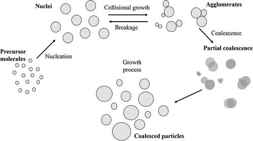
In gas phase synthesis, nanoparticles are made by ‘building’ them from individual atoms or molecules up to the desired size: cluster embryos are formed either by physical means such as condensation of a supersaturated vapor or by chemical reaction of gaseous precursors [Citation24,Citation25]: shows schematically the nanoparticle growth process. Depending on the embryo concentration, system temperature and pressure, clusters continue to grow to larger entities by coagulation and coalescence and/or surface growth, finally forming a suspension of particles in a gas (aerosol) [Citation24,Citation48]. The starting material can be vaporized from a hot source into a low-density inert gas employing Joule heating, laser ablation, arc discharge or sputtering [Citation24,Citation25,Citation49].
Figure 2. Schematic representation of nanoparticle growth processes in the gas phase. The precursor from which the growth starts are molecule or atoms dispersed in an inert gas. Nucleation processes form the first agglomerates. Collisional phenomena tend to increase the size or to break the preformed agglomerates
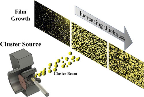
Different cluster production techniques are more or less suitable for scale-up, while maintaining a tight size distribution and/or chemical composition: aerosol sources can produce nanoparticles in bulk quantities, but they have the drawback of a limited control of particle size distribution and on particle manipulation in the gas phase resulting in a poor control of lateral resolution of the deposited particles [Citation24]. High lateral resolution can be obtained by cluster beam deposition based on supersonic gas expansion techniques [Citation50], is a schematic of a typical cluster-beam deposition (CBD) process.
Figure 3. Schematic view of a deposition process of clusters to grow nanostructured metallic films. Metal clusters are produced in a suitable source and subsequently deposited on a substrate
The sputtering of a target in the presence of an inert gas is one of the most popular and widely used methods to produce metal cluster beams [Citation51]. The coupling of a magnetron plasma source to a gas-aggregation cell for CBD has been proposed by H. Haberland and co-workers [Citation52]: in the original design, the magnetron discharge is operated at a pressure of about 1 Torr to favor aggregation of the sputtered species; clusters are carried away from the formation region by the gas stream. Sputtering sources produce a large amount of ionized clusters that can be accelerated in a second chamber towards a biased substrate. By varying the distance between the magnetron unit and the orifice, the cluster residence time and hence the mass distribution can be controlled [Citation24,Citation53].
This approach has been developed and refined along the last couple of decades to achieve a very good control on structure and stoichiometry of the produced clusters; considerable efforts have been also directed toward an increase of production rate and cluster manipulation after the extraction for the source [Citation24]. Deposition rates depend on the different sputtering source designs and the growing parameters used such as geometry of the vacuum chambers, carrier gas pressure, the ionization degree of the nanoparticles, etc. [Citation53]. Despite significant progress, magnetron sputtering remains a technique limited by a rather low cluster deposition rate [Citation51], basically due to the difficulty of efficiently extracting the nanoparticles from the condensation region of the source [Citation53]. The continuous working regime, typical of this class of sources, severely limits the use of supersonic expansions as a tool for cluster manipulation and focusing in flight [Citation25,Citation53].
An interesting evolution of CBD is represented by supersonic cluster beam deposition (SCBD) that has been demonstrated as a scalable fabrication tool up to industrial processes currently in use [Citation49,Citation54]. SCBD is characterized by a high deposition rate, high lateral resolution (compatible with planar microfabrication technologies) and neutral particle mass selection process by exploiting aerodynamic focusing effects [Citation24]. SCBD is an enabling tool for the large-scale integration of nanoparticles and nanostructured films on microfabricated platforms and smart nanocomposites [Citation55]. A typical SCBD apparatus is schematically shown in .
Figure 4. Schematic view of a SCBD apparatus: clusters are produced in the source chamber (equipped with a PMCS) and extracted thought a supersonic expansion (yellow beam in the figure). The beam is focused in the expansion chamber and directed into the deposition chamber through a skimmer. Samples are fixed on a mobile holder (manipulator) with six faces that can be exposed to the cluster beam. Top left: PMCS structure
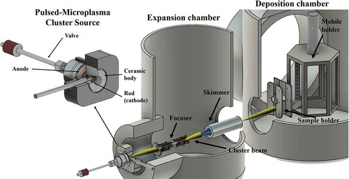
A source particularly suited for the production of intense and stable neutral supersonic cluster beams is the pulsed microplasma cluster source (PMCS), as described in details in [Citation56,Citation57]. Briefly, the PMCS principle of operation consists on the ablation of a metal target rod by a plasma ignited during the injection of a high-pressure pulse of an inert gas (He or Ar) [Citation56,Citation57]. The species resulting from the target ablation condense through collision with the inert gas to form clusters, then the cluster-gas mixture is expanded through a nozzle generating a supersonic seeded beam [Citation58]. The cluster beam is focused by an aerodynamic lenses system [Citation59] and directed on a substrate placed in a deposition chamber. A quartz microbalance periodically monitors the amount and the rate of deposited material and it allows to make an estimation of the nominal thickness of the films. High directionality, collimation and intensity of aerodynamically focused supersonic cluster beams make them well suited for patterned deposition of nanostructured films through non-contact stencil masks or lift-off technologies [Citation60,Citation61].
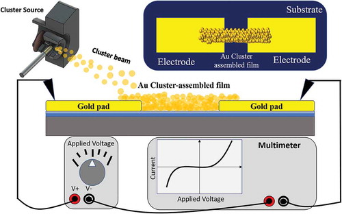
The efficient decoupling of cluster production, manipulation and deposition in a typical SCBD apparatus allows the in situ characterization of the evolution of the electrical properties of cluster-assembled films during the fabrication process: in we show schematically the configuration of the substrate holder for the in-situ electrical two-terminal device: the cluster assembled film is deposited by using a stencil mask [Citation42,Citation43].
Figure 5. Schematic representation (not to scale) of a sample holder mounted on the manipulator during the cluster deposition process through a stencil mask. Substrates are connected in series with a digital multimeter remotely controlled by a computer for the in situ characterization of the resistance evolution
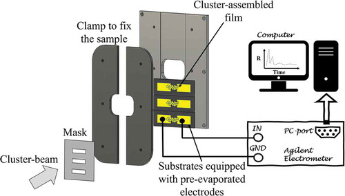
The sample holder is equipped with electrical contacts for the in situ characterization of the evolution of the electrical properties of the film during the deposition process. To perform electrical measurements, the substrate has to be equipped with pre-deposited metallic electrodes. The substrate is placed in on a support and fixed through two lateral clamps. The mask is situated on the support to intercept the cluster beam and pattern the deposited film.
Cluster-assembled films deposited on microfabricated substrates can be also electrically characterized ex situ. In the simplest case of two-probe configuration, the sample is connected in series with a digital multimeter, a voltage is applied and the current flowing in the device is measured to compute the resistance as the ratio between the voltage and the current. The resistance measurement can be repeated at variable frequency under the application of a constant voltage and for ramped voltage values.
3. Growth of nanostructured metallic films
The presence and the evolution of defects in metallic thin films, depending on their thickness and growth conditions, have important consequences on the electrical conduction properties, in particular, with a significant increase of resistivity values compared to the corresponding bulk materials [Citation35,Citation36,Citation62,Citation63]. Electric transport in polycrystalline thin films characterized by a high number of defects and grain boundaries has been extensively explored due to the need of extremely high integration of devices and hence the reduction of the dimensions of interconnects [Citation64–66].
Here we consider the growth mechanisms of cluster-assembled films with particular focus on the differences from the growth of atom-assembled metallic films and on the factors that can influence and determine their morphological properties at the nanoscale.
3.1 Background: atom-assembled metallic films
Polycrystalline thin films, grown by atom assembling exhibit a wide variety of microstructures characterized in terms of grain size and crystallographic orientation, lattice defects, phase composition, and surface morphologies [Citation67–69]. The Volmer-Weber model describes the initial growth stages characterized by the formation on the substrate of isolated islands with sizes and shapes strongly dependent on surface and bulk diffusion [Citation70]. The grains formed on the substrate in the first stages increase their lateral size with the thickness: the film microstructure typically evolves in a competitive fashion and the kinetic limitations typical of growth conditions far from thermodynamic equilibrium causes the formation of metastable phases and defects on the micro- and nanoscale [Citation67,Citation71,Citation72].
The growth processes controlling microstructural evolution include nucleation, island growth, coalescence of islands, formation of polycrystalline domains, development and growth of a continuous structure. When surface diffusion rates are significant, film thickening proceeds through local epitaxy on individual grains. Grain coarsening, i.e. recrystallization through grain boundary can occur both during and after island coalescence [Citation67,Citation73].
The nucleation barrier is generally expected to be small, leading to randomly oriented islands, for low-temperature deposition on amorphous substrates [Citation74]. During island coalescence, there is a strong driving force for coarsening through surface atom diffusion and grain boundary motion. The island with lower energy per atom consumes the others, resulting in a new single-crystal island as the system attempts to minimize the overall surface and interface energy. Coarsening during coalescence is the first and most active phenomenon leading to selection of preferred orientation [Citation67,Citation73].
With continuing deposition, the islands grow until they come into contact forming a metallic network which then ‘in-fills’ to form a continuous film. The dimension of the grains in such a type of metallic film usually increases with the average thickness in a wide range of thickness values (from few to hundreds of nanometers) [Citation68,Citation75]. As we will discuss in the following, this is the main differences with respect to a cluster-assembled film where the number of defects and grain boundaries does not depend from the film thickness.
3.2 Cluster-assembled film growth
Although one can expect that the use of clusters as building blocks causes substantial differences in the morphology, structure and functional properties of metallic nanostructured films, compared to the atomic deposition [Citation34], only very recently these aspects have been explicitly highlighted [Citation42–44].
The growth of cluster-assembled metallic films has been studied mainly in the sub-monolayer regime with particular focus on transition metal clusters [Citation76,Citation77], noble metals [Citation42,Citation78–80], bismuth [Citation81–83], tin [Citation84] and antimony [Citation85,Citation86]. Nucleation and growth process of Bi and Sb thin films grown by atomic and cluster deposition has been characterized by transmission electron microscopy (TEM) showing the high sensitivity of the film structure to the size of incident precursors [Citation34,Citation81]. The increase of the size of incident clusters induces a decrease of the mean diameter of the supported aggregates; when the size of free low-energy clusters increases, their surface diffusion becomes low enough to neglect the growth of supported particles [Citation34].
The growth by CBD of antimony films has been modelled as the filling of a random network in the percolation model. This allows quantitative predictions of the electrical conduction threshold (as we will discuss in the next paragraph), coverage rate at the threshold, fractal dimension of the percolating path and multifractal properties of the cluster-assembled films [Citation34].
Transition metal nanostructured films grown by SCBD have been characterized by AFM [Citation77]. In , the typical surfaces of W, Mo, and Fe cluster-assembled films, measured ex-situ by AFM, are reported. The observed morphology is characterized by nanoscale porosity, poorly connected and non-compact structures with lower density with respect to bulk and a surface roughness increasing with film thickness.
Figure 6. (a) Surface morphologies of cluster-assembled W, Mo and Fe taken by AFM (the side of the images correspond to 1 µm; the thickness of the films is few tens of nm). The morphologies of W, Mo and Fe films look very similar, indicating similar cluster dimensions and similar growth dynamics. From [Citation77]
![Figure 6. (a) Surface morphologies of cluster-assembled W, Mo and Fe taken by AFM (the side of the images correspond to 1 µm; the thickness of the films is few tens of nm). The morphologies of W, Mo and Fe films look very similar, indicating similar cluster dimensions and similar growth dynamics. From [Citation77]](/cms/asset/d33b0af7-899e-4db0-81b1-351d05185e5e/tapx_a_1908847_f0006_b.gif)
The growth processes of cluster assembled gold films have also been studied starting from the sub-monolayer regime () on HOPG [Citation80]. The evolution of the cluster density can be described by a ballistic deposition model [Citation32], cluster coalescence or re-arrangement is not observed demonstrating that the crystalline structure of the preformed clusters is conserved upon deposition and that no evolution of grain boundaries is present [Citation33,Citation79,Citation80].
Figure 7. Scanning tunnel microscopy images 100 × 100 nm2 of the morphologies of Au cluster films on Au111 surface for different equivalent thickness Eq. (a) Eq = 0.01 nm; (b) Eq = 0.03 nm; (c) Eq = 3.4 nm. Supported cluster size varies weakly with the equivalent thickness. All the observations have been performed with the same tip, a gap voltage of 0.3 V and a tunnelling current of 1 nA. From [Citation80]
![Figure 7. Scanning tunnel microscopy images 100 × 100 nm2 of the morphologies of Au cluster films on Au111 surface for different equivalent thickness Eq. (a) Eq = 0.01 nm; (b) Eq = 0.03 nm; (c) Eq = 3.4 nm. Supported cluster size varies weakly with the equivalent thickness. All the observations have been performed with the same tip, a gap voltage of 0.3 V and a tunnelling current of 1 nA. From [Citation80]](/cms/asset/ce44cbb2-fad1-450f-a122-09d09204a176/tapx_a_1908847_f0007_b.gif)
A systematic characterization of the growth process of nanostructured films produced by SCBD from sub-monolayer to thickness of hundreds of nanometers has been reported [Citation87]. The process of film formation takes place in a ballistic deposition regime [Citation32], consequently, the deposition time is the main parameter that allows for the control of the film surface morphology that evolves regularly according to simple and reproducible scaling laws [Citation88].
Since the cluster mass distribution prior to deposition strongly affects the growth dynamics [Citation32,Citation45], the geometrical properties of the gold clusters deposited on a surface were studied in the case of sub-monolayer regime. ) reports the height distribution of gold clusters (diameter in z direction, i.e. normal to the substrates) for a film with coverage ∼8%. The results show a broad distribution with height peaked at 0.4 ± 0.1 nm, while the median value of the largest cluster population is around 6 ± 2.5 nm. A dimension analysis was also performed on sub-monolayer SEM images: the equivalent radius distribution is bimodal, with the main two peaks around 0.7 and 4.4 nm.
Figure 8. Dimensional analysis of cluster-assembled gold film. From left to right: histogram in logarithmic scale of the height of the clusters measured by AFM of sub-monolayer sample (coverage 8%). (b) relative island heights (measured by AFM) and the relative radius (measured from SEM micrographs) as a function of the coverage. (c) histogram of the equivalent radius of the grains obtained segmenting a SEM micrograph of the film 60 nm thick, in logarithmic scale. Adapted from [Citation42]
![Figure 8. Dimensional analysis of cluster-assembled gold film. From left to right: histogram in logarithmic scale of the height of the clusters measured by AFM of sub-monolayer sample (coverage 8%). (b) relative island heights (measured by AFM) and the relative radius (measured from SEM micrographs) as a function of the coverage. (c) histogram of the equivalent radius of the grains obtained segmenting a SEM micrograph of the film 60 nm thick, in logarithmic scale. Adapted from [Citation42]](/cms/asset/e7979ef2-7f06-49a2-a27b-29f4e8e8936f/tapx_a_1908847_f0008_oc.jpg)
The study was carried out increasing the surface coverage from 8% to 45% [Citation42]. shows the trend of the relative island heights and their relative radius as function of the coverage percentage. The mean value of the whole clusters heights increases of only 50%, on the other hand, the equivalent radius increases of 160% (). This suggests a preferential growth in x-y directions instead of z one, in the first growth stages caused by the highest mobility of the small clusters. The surface diffusion on the substrate and the nucleation are favored for smaller clusters resulting in a 2D growth, while larger clusters act as static nucleation sites where a 3D growth mode is promoted.
At 70% coverage, 3D growth takes place: above this threshold, cluster diffusion is strongly hampered, irrespective of the incident cluster dimension. The growth regime is now fully ballistic. The study shows a strong difference with the structural properties of gold films assembled by atoms. Cluster-assembled gold films are still characterized by a grain distribution substantially similar to that of the sub-monolayer regime (quantitative granulometric characterization from SEM images is reported in ) [Citation32,Citation87]. This is further confirmed by a morphological analysis with atomic force microscopy (AFM) of the continuous cluster-assembled films. In , the histogram of the grain dimensions resulting from the quantitative granulometric characterization [Citation32] is reported. The grain size distribution nearly perfectly overlaps to that of the sub-monolayer film, thus confirming that no significant grain growth is present even for very large thicknesses [Citation80], at odd to what observed for the growth of gold films assembled by atoms [Citation68,Citation75].
High-resolution TEM (HRTEM) characterization of cluster-assembled gold films () shows that all the islands formed by the aggregation of gold clusters are crystalline and that the larger ones have a morphology composed by several crystal domains with no preferential orientation [Citation89].
Figure 9. TEM/HRTEM micrographs of cluster-assembled gold films. (a) overall view of the percolating film, scale bar: 250 nm; (b) magnified view of the square reported in panel (a), scale bar: 100 nm; (c) magnified view of the square reported in panel (b), scale bar: 50 nm; (d) HRTEM image of a polycrystalline aggregate surrounded by the square in panel (c), scale bar: 10 nm. From [Citation44]
![Figure 9. TEM/HRTEM micrographs of cluster-assembled gold films. (a) overall view of the percolating film, scale bar: 250 nm; (b) magnified view of the square reported in panel (a), scale bar: 100 nm; (c) magnified view of the square reported in panel (b), scale bar: 50 nm; (d) HRTEM image of a polycrystalline aggregate surrounded by the square in panel (c), scale bar: 10 nm. From [Citation44]](/cms/asset/96d39427-b895-42d1-bf02-8040addc602d/tapx_a_1908847_f0009_b.gif)
The islands forming the film consist of several crystalline domains, with size (calculated as domain wall length) ranging between 5 and 10 nm. They are randomly organized in crystalline orientations: some of them are twinned domains, while in other cases the domains are separated by grain boundaries, often with frequent stacking faults. In some cases, a superposition of crystal domains is also observed, as confirmed by the presence of Moiré fringes ().
shows the values of the mean grain size of three Au cluster-assembled films with increasing thickness and the theoretical grain size growth for atom assembled films [Citation68,Citation75]. The grain size of a nanostructured film remains substantially constant, on the contrary that of a film assembled by atoms strongly increases for thickness greater than a certain threshold (about 40 nm). In the case of atom-assembled films, the islands grow through nucleation or coalescence processes, determining a lateral increasing of the grain size [Citation70,Citation75]. Cluster-assembled films are characterized constant dimensions of the grain size due to the stability against coalescence of the deposited clusters [Citation80], this causes the presence of an extremely high density of grain boundaries. In a HRTEM image of a sub-monolayer region of a typical gold cluster-assembled film is shown.
Figure 10. Left) Mean grain size as function of thickness for a cluster-assembled (red dots) and an atom-assembled film (blue asterisks, data from [Citation68]). (Right) HRTEM image of a typical region of a sub-monolayer cluster-assembled gold film. Different crystal domain separated by grain boundaries are visible. For each single crystal domain, the corresponding zone axis [hkl] is displayed, after determination by local 2D-Fourier analysis of the relevant region of interest in the HRTEM image. From [Citation44]
![Figure 10. Left) Mean grain size as function of thickness for a cluster-assembled (red dots) and an atom-assembled film (blue asterisks, data from [Citation68]). (Right) HRTEM image of a typical region of a sub-monolayer cluster-assembled gold film. Different crystal domain separated by grain boundaries are visible. For each single crystal domain, the corresponding zone axis [hkl] is displayed, after determination by local 2D-Fourier analysis of the relevant region of interest in the HRTEM image. From [Citation44]](/cms/asset/dbf2b0ce-6f54-44f4-9091-4489b01d6ed5/tapx_a_1908847_f0010_oc.jpg)
The structure of cluster-assembled films due to the survival of the original precursors structure has also been reported in other studies considering the evolution of isolated gold clusters deposited on gold surfaces [Citation79,Citation90] and in the characterization of the optical properties of cluster-assembled gold films [Citation33].
4. Electrical transport in nanostructured metallic films
4.1 Percolation theory
Percolation theory describes the correlation between the morphological properties and the electrical conduction of nanogranular metallic films [Citation37,Citation39,Citation91]. The notion of percolation is related to the study of paths formed by the elements composing a system: one can consider a lattice where a particle is represented by an occupied site ( panel a): the percolation threshold is reached when at least a continuous path formed by contiguous occupied sites appears.
Figure 11. (a) Schematic representation of the percolation onset in a 2D lattice with a fraction of occupied sites (in black). From [Citation92]. (b) Schematic evolution of the percolation curve, showing the change in conductivity of a metallic thin film as function of its thickness
![Figure 11. (a) Schematic representation of the percolation onset in a 2D lattice with a fraction of occupied sites (in black). From [Citation92]. (b) Schematic evolution of the percolation curve, showing the change in conductivity of a metallic thin film as function of its thickness](/cms/asset/8e36c009-9b8e-4870-b403-ca29722e43e5/tapx_a_1908847_f0011_oc.jpg)
The percolation theory can describe many aspects of the evolution of different physical systems: porous media, spread of diseases and fires, gelation and glass transitions [Citation93]. In particular, the percolation formalism has been used to describe the thin-film growth process from discontinuous to continuous states [Citation76,Citation83,Citation94], the metal/insulator transition in nanocomposites [Citation39] and the divergence of electrical conductivity and dielectric constant in sintered composites consisting of micrometer-sized powders [Citation37].
In the case of the evolution of the electrical conductivity of metallic films as function of their thickness, the system undergoes through three electrical conduction stages: an insulating one, where only isolated aggregates are present on the substrate; the percolation stage, where the film is still discontinuous but the islands begin to join, forming conductive paths; the continuous stage, where a continuous conducting layer is formed ( panel b).
Near the percolation threshold, the electrical conductance G obeys a power law,
where p is the fraction coverage andis the critical faction, two quantities strictly related to the thickness [Citation37]; the exponent q has a universal value and it depends only on the dimensionality of the system. A conspicuous number of experimental results demonstrated that the conduction properties of metallic thin films are related to percolation and that the metal insulator transition belongs to the same universality class of the percolation problem [Citation39].
When granular systems formed by metal clusters are considered, some care must be taken with the concept of geometrical contact. In particular, standard percolation theory considers the conducting particles as either electrically connected, with some finite inter-particle conductance, or disconnected [Citation20,Citation39]. A sharp cut-off applies well only to composites made of large conducting particles (in the micrometric scale), for which two particles can be considered electrically connected only if they touch each other [Citation20]. When a nanostructured system is formed by elements and structures having sizes limited to a few nanometers, the presence of this sharp cut-off is less clear. In the insulator–conductor transition region, metal particles begin to touch each other, leading to the formation of conductive paths. In this regime, nanogranular systems exhibit a feature common to most random insulator-conductor mixtures, once a critical volume fraction of the conductive phase is reached, a sharp increase of the conductivity is observed. The electrical conductivity is due to both percolation along the forming metallic network and electron tunnelling between isolated particles. By further increasing the volume fraction of the metal fillers, tunnelling or hopping effects become less and less important compared to the contribution of percolation [Citation95,Citation96].
Once a continuous layer is formed, an ohmic-type conduction regime is reached; however, the presence of an extremely high number of defects and grain boundaries typical of cluster-assembled films regardless the thickness may have a profound influence on the conduction regime [Citation44]. The role of defects on electrical conduction of polycrystalline thin film has been extensively studied, much less is known about cluster-assembled nanostructured film. As we will show, an extrapolation of the polycrystalline film behaviour to the nanogranular case is not justified by recent experimental results [Citation42–44].
4.2 Electrical transport in polycrystalline metallic thin films
The electrical transport properties of polycrystalline metallic thin films are profoundly affected by the presence of defects and grain boundaries [Citation35,Citation36,Citation68,Citation97]. In standard growth conditions, the density of grain boundaries decreases with increasing film thickness: major efforts have been concentrated in identifying growth conditions where the number of defects is minimized in view of miniaturization of electronic circuits [Citation40].
The early stages of film growth by atom assembling are characterized by the formation of isolated islands on the substrate [Citation98]. The description of the electrical conduction mechanism at this stage is difficult since the experimental observations are averaged on the whole film constituted by several isolated aggregates [Citation99]. The main phenomena involved are tunnelling process, temperature activated conduction and Shottky processes [Citation95,Citation96]. Charging effects of the isolated islands can play an important role due to the wide distribution of island sizes and interspacing distancing that causes fluctuation of tunnel gaps and charging energies [Citation95,Citation96].
As the average thickness of the films increases up to a critical value tc percolation threshold is reached, the isolated islands merge forming continuous paths and the film undergoes to metal-insulator transition [Citation37]. Near the percolation region the structure of the film is characterized by a complex network of connected aggregates with irregular and ramified shape, the electrical conduction is strongly non-linear [Citation69,Citation95,Citation96]. The complex electrical behaviour can be described by the model developed for nanocomposite systems consisting of metallic nanoparticles embedded in a dielectric matrix [Citation37,Citation91], note that in the literature these systems are referred as granular films, thus causing confusion with single-phase metallic systems composed by micro- or nanoscale metallic building blocks without a non-conducting matrix.
The electrical conduction of continuous metallic films (beyond the percolation threshold) is in the ohmic regime; however, resistivity slightly evolves with film thickness and it shows significant departures from the bulk values [Citation100]. Several models were developed to integrate in the classical theories of Drude and Sommerfeld for the metallic conduction, the dimensionality effect due to the presence of the surface, the grain boundaries and a higher concentration of defects with respect to bulk materials [Citation35,Citation36,Citation40,Citation62,Citation97].
The three principal scattering sources affecting the electron motion in polycrystalline metallic films are: 1) the scattering inside the single grain region (the volume or background scattering), 2) the scattering at the grain boundaries and 3) the scattering near the surfaces [Citation100]. The conduction of continuous metallic films with thickness comparable to the conduction electron mean free path is described by the Fuchs-Sondheimer (FS) model [Citation35,Citation97].
In the FS model, the resistivity dependence on film thickness is related to diffusively electron scattering at the film boundaries that essentially imposes a restriction on the electronic mean free path [Citation35,Citation97]. Since the resistivity is inversely proportional to the mean free path, it consequently increases with the decreasing of the film thickness. The thin film surfaces are the only confinement structure playing a morphology-related role on electron scattering; hence, the model provides good explanations of single-crystal thin film resistivity.
The film conductivity as function of the thickness
was derived by modelling the surface scattering in the Boltzmann transport equation as a special boundary condition for the electron velocity [Citation35,Citation97]:
where p is the fraction of electrons elastically reflected at the surfaces, against the fraction 1-p that is diffusively scattered, and the mean free path of an infinite thick film and
the bulk conductivity. Two simplified expressions were given by Sondheimer [Citation35] in the limit of thick film (
)
and in the limit of thin film ()
The role of surface roughness was considered into other models like those in [Citation101]. shows experimental measured resistance values of different metal films compared to theoretical calculation of the Fuchs-Sondheimer model. The theoretical model usually overestimates the experimental data.
Figure 12. Electrical resistivity vs. film thickness measured for Al, Au and Cu polycrystalline films. From [Citation75]
![Figure 12. Electrical resistivity vs. film thickness measured for Al, Au and Cu polycrystalline films. From [Citation75]](/cms/asset/e71eb4ec-326d-4f45-bf6a-3eb39b103c98/tapx_a_1908847_f0012_b.gif)
Mayadas and Shatzkes [Citation36] introduced the grain boundaries effect in the FS model. The key of their work lays in the observation that up to film thicknesses of the order of 1 micron, the mean grain diameter is approximately equal to the film thickness, due to the growth mechanism of atom-assembled thin films [Citation68,Citation75]. The grain boundaries are modelled like parallel and equally spaced planes, perpendicular to the electric field responsible for the electron motion. In the proximity of each plane, a short-range and smooth potential produce a perturbation to the electron motion, so that only specular reflection is produced. Following the method previously described, the Boltzmann transport equation is solved for this problem [Citation36,Citation40] to find the expression for the conductivity due to grain boundary.
Hofmann and co-workers proposed an alternative calculation of the conductivity of thin metallic films including the contribution of grain boundaries scattering [Citation102]. The grain boundary potential is introduced in the Schrodinger equation in the form of a series of potential barrier that electron goes through along its mean free path. This model brings to a modified Drude formula [Citation62]:
where, is the transmission coefficient,
is the Fermi velocity,
is the mass of the electron,
is the grain size and
the electron density of a bulk material without grain boundaries. The formula can be interpreted considering that only a fraction
of the bulk electron density gives a contribution to the conductivity [Citation62,Citation100].
This model highlights the contribution of grain boundaries on the electron conduction, as the different ratio between grain size and mean free path length can have different consequences (like a negative temperature coefficient of the resistance) [Citation62,Citation103].
Although the above mentioned models consider the possible scattering sources in a metallic film and well approximate the continuous region of the percolation curve, they do not give an exhaustive answer to the description of the conduction in nanostructured metallic films. The weak point is represented by the concept of mean free path that can be difficult to define in metallic films where the grain boundary reaches a high density, as is the case in cluster-assembled films [Citation102,Citation104].
This brings us to a second critical aspect: all the models do not suitably consider the role of disorder. In fact, nanoscale grains do not have the same dimensions and are not equally spaced, although they are modelled like a periodic potential [Citation40] and only a posteriori mean grain size is taken to predict the experimental data [Citation102]. It is well known that a disordered potential can cause localized states and that the electrical transport may be strongly influenced [Citation105–107].
4.3 Electrical transport properties of cluster-assembled metallic films
In cluster-assembled metallic films, the nanoscale building blocks maintain their individuality during the growth process causing a very large density of grain boundaries and defects that does not decrease with the film growth [Citation43,Citation44]. This aspect was only recently recognized since in the past the evolution of the electrical conduction has been studied at very low coverage up to the electrical percolation threshold. In this low-coverage regime electrical conduction behavior analogous to what observed for atom-assembled films has been reported; the differences in the percolation curve evolution have been attributed to the different diffusivity and coalescence regime typical of clusters [Citation34].
K. Sumiyama and co-workers, reported, for sub-monolayer Co cluster-assembled films, a dependence of the electrical conductivity percolation curve exponent from the cluster size distribution [Citation76]. The interactions among clusters and the parameters of deposition can determine a growth process and conduction properties that are not fully explained by a simple scaling law. The authors proposed the occurring of conductivity distribution among clusters to explain the observations [Citation76].
The characterization of the electrical percolation of cluster-assembled Sb films revealed that the evolution of the electrical properties during the growth was substantially different from the case of atom deposition, suggesting a role of the film morphology in the development of the electrical properties of the nanostructured layers [Citation34,Citation108].
S. Brown and co-workers demonstrated the electrical switching behaviour and quantized conductance at room temperature in percolating films of metal-oxide nanoparticles [Citation109]. They showed that percolating systems of randomly deposited nanoparticles exhibit room temperature quantized conductance and switching, both during, and in response to, applied voltages. They attributed this behaviour to the formation of atomic-scale wires within the gaps in the film of particles [Citation110]. The characteristics of this percolating-tunnelling systems may be exploited for the fabrication of neuromorphic devices [Citation109].
Studies on the electrical transport properties of continuous nanostructured films built from bare metallic clusters were substantially absent due to the lack of cluster sources able to provide intense and stable beams for the fabrication of ‘thick’ films; a paper on continuous cluster-assembled silver films reported about the observation of an ohmic behavior similar to the case of polycrystalline films [Citation78]. In general, the role of defects was not investigated systematically.
The use of SCBD equipped with PMCS allowed a systematic characterization of the electrical conduction of metallic cluster-assembled films with thicknesses larger than the percolation threshold [Citation42,Citation77].
The in-situ evolution of the electrical resistivity of Fe, Pd, Nb, W and Mo cluster-assembled films has been reported [Citation77]. shows their resistivity evolution: resistivity values of 3–4 orders of magnitude higher than bulk ones for all metals can be observed, and a non-monotonic evolution with thickness, with a local minimum around 5–6 nm is present. Remarkably, the resistivity of cluster-assembled films shows an increasing asymptotic trend with growing thickness instead of a decreasing trend converging to bulk values, as for atom-assembled films. The resistivity of the various metals increases according to a power law, as highlighted by the constant slope in the log-log plot.
Figure 13. Percolation curves of cluster-assembled films for different materials obtained plotting the resistivity as a function of thickness. The non-monotonic behavior can be ascribed to structural evolution occurring in the cluster-assembled film during growth. From [Citation77]
![Figure 13. Percolation curves of cluster-assembled films for different materials obtained plotting the resistivity as a function of thickness. The non-monotonic behavior can be ascribed to structural evolution occurring in the cluster-assembled film during growth. From [Citation77]](/cms/asset/e81b7688-50ac-4e59-9d68-f0af5f42f583/tapx_a_1908847_f0013_oc.jpg)
The calculated exponents of power-law are: 0.41 for Pd, 0.70 for W, 0.78 for Fe and Nb. Note that between 5 and 10 nm, Mo and W have resistivities higher than other metals, opposite to what happens in bulk. The increasing asymptotic trend of resistivity can be explained by considering that cluster-assembled films have 3D growth dynamics ascribable to the ballistic regime where the progressive decrease in the topological connection of the uppermost layers is observed [Citation111]. The uppermost layers of the growing film are less compact and hence less conductive due to the decreasing percolative path density caused by minimal cluster interconnection and morphologies related to the ballistic growth regime [Citation111]. Similar effects have been reported for nanogranular systems fabricated by the assembling nanoparticles produced in aerosols [Citation112].
Cluster-assembled gold films are of particular interest since they are not affected by oxidation of the nanoparticles during and after the deposition process. As observed for other cluster-assembled systems, the grain structure at the nanoscale is not influenced by the aggregation process with other particles.
The non-linear electrical behavior and the presence of resistive switching phenomena have been reported in cluster-assembled gold films below the percolation threshold [Citation46].
Figure 14. Top: percolation curves of an atom-assembled gold film (blue) and of a cluster-assembled film (red). The curves show the evolution of the conductance as a function of the film thickness. Bottom: SEM images of films at different coverages showing the evolution of their morphologies: A) continuous atom-assembled film (scale bar 200 nm). B-D: Images of the principal steps of growth of a cluster-assembled metallic films are reported counter-clockwise: B) insulating stage; C) close to percolation; D) conducting regime: a fully connected thick-film (scale bar 100 nm). From [Citation42]
![Figure 14. Top: percolation curves of an atom-assembled gold film (blue) and of a cluster-assembled film (red). The curves show the evolution of the conductance as a function of the film thickness. Bottom: SEM images of films at different coverages showing the evolution of their morphologies: A) continuous atom-assembled film (scale bar 200 nm). B-D: Images of the principal steps of growth of a cluster-assembled metallic films are reported counter-clockwise: B) insulating stage; C) close to percolation; D) conducting regime: a fully connected thick-film (scale bar 100 nm). From [Citation42]](/cms/asset/79719fa0-71d8-4a90-80f0-89743fd2e306/tapx_a_1908847_f0014_oc.jpg)
shows the evolution of the electrical properties of a typical cluster-assembled Au film (red curve) compared to that of an atom-assembled one (blue curve) measured in situ during deposition. The scanning electron microscopy (SEM) images () are associated with the fundamental stages of the percolation curve [Citation42].
The three principal growth stages of the random assembling of nanoparticles are easily identified from the conductance-thickness curve. The evolution of the conductivity of cluster-assembled films with thickness (, red curve) shows that for a film characterized by isolated aggregates, an insulating behavior is observed [Citation42]. By increasing the thickness, the first percolation paths are formed (geometrical percolation stage) the conductivity abruptly increases, while the film is still in sub-monolayer regime. The critical thickness for the electrical percolation threshold, corresponding to the film morphology in , can be determined by the occurrence of the maximum slope of the conductivity vs. thickness curve [Citation113]. After the percolation transition, the cluster-assembled film is fully connected (); however, differences between the atom-assembled and the cluster-assembled systems are evident [Citation42].
Figure 15. A) Electrical resistance and current of an atom-assembled Au film, 100 nm thickness, as a function of time under the application of 0.5 V. b) electrical resistance and current of a cluster-assembled Au film, 65 nm thickness, as a function of time under the application of 12 V. c) I–V curve of a cluster-assembled film after the activation of the switching activity in semilog-y scale. From [Citation42]
![Figure 15. A) Electrical resistance and current of an atom-assembled Au film, 100 nm thickness, as a function of time under the application of 0.5 V. b) electrical resistance and current of a cluster-assembled Au film, 65 nm thickness, as a function of time under the application of 12 V. c) I–V curve of a cluster-assembled film after the activation of the switching activity in semilog-y scale. From [Citation42]](/cms/asset/e657de68-021f-4baa-bdf2-47193ca69323/tapx_a_1908847_f0015_oc.jpg)
For the sake of comparison, in the evolution in time of the measured electrical resistance under a constant voltage is reported both for an atom assembled (panel a) and a cluster assembled film (panel b) in the continuous regime. Cluster-assembled films are characterized by a higher initial resistance compared to the atom-assembled ones; for this reason, a larger voltage drop in the former is observed, for the same current circulating in both systems. The difference in the resistivity values between atom-assembled and cluster-assembled films is due to the presence of an extremely large number of defects and grain boundaries typical of the low-energy cluster beam deposition regime resulting in highly porous films [Citation42].
The behaviour of the continuous Au cluster-assembled film is non ohmic and characterized by a discrete variation of the resistance (see ) and by the onset of switching activity with a series of discrete and reversible resistance variations. Remarkably the I–V curve of the cluster-assembled film shows a non-linear behavior and the presence of hysteresis.
Gold cluster-assembled films present a stable resistive switching behavior with well-defined resistance levels that are recurrently explored under the application of a constant voltage bias, and whose order of magnitude depends by the applied voltage (see and ). In this regime, the I–V curves appear to be non-Ohmic, as shown in .
Figure 16. Example of resistive switching behaviour in cluster-assembled gold films. a) electrical resistance of a film with thickness of 30 nm under a bias of 20 V; b) histogram of the resistance values under the application of 20 V in a time window of 200 s. c) electrical resistance of the same sample under a bias of 0.5 V. d) histogram of the resistance values of the sample under the application of 0.5 V in a time window of 200 s. From [Citation42]
![Figure 16. Example of resistive switching behaviour in cluster-assembled gold films. a) electrical resistance of a film with thickness of 30 nm under a bias of 20 V; b) histogram of the resistance values under the application of 20 V in a time window of 200 s. c) electrical resistance of the same sample under a bias of 0.5 V. d) histogram of the resistance values of the sample under the application of 0.5 V in a time window of 200 s. From [Citation42]](/cms/asset/cf33ec3f-fee0-47d8-9162-dea5fcccba42/tapx_a_1908847_f0016_oc.jpg)
reports the evolution of the resistance for a cluster-assembled film with a thickness of 30 nm under the application of 20 V bias after the activation: typical switching features are present, consisting in reversible switches in different resistance ranges. This is quantitatively represented in reporting the histogram of the resistance values under a bias of 20 V in a time window of 200 s. The histogram shows different Gaussian type peaks around each resistance values reached after the switch events occur.
In cluster-assembled gold films, the granular structure at different length scales largely determines the non-ohmic electrical properties of the system. Although the elemental building blocks can be considered metallic, their assembly does not result in an overall ohmic conductor. The use of ‘good metal’ building blocks to fabricate ‘bad metal’ systems has been reported in the case of Ag films, assembled with traditional methods, where structural disorder at the mesoscale influenced in a substantial way the electronic properties of the system [Citation104].
Electronic carrier conduction in nanostructured systems can be considered to be based on space charge limited conduction mechanisms and coulomb blockade [Citation95,Citation114] with very strong geometrical constraints [Citation96,Citation115,Citation116]. The presence of an extremely high density of grain boundaries and crystalline orientation mismatch deeply affect the electrical conduction [Citation65,Citation104,Citation117,Citation118] representing a barrier for the electric charge flow determining and resulting in a distribution of different ‘resistances’ over the cluster-assembled film [Citation119].
As a result, the current flowing and the energy dissipation can give rise to rearrangement phenomena at the grain boundaries. The momentum exchange between the flowing electrons and the atoms can cause the rearrangement phenomena and locally changes the resistance. The current redistribution will trigger other events. The process, schematically shown in , qualitatively represents, in three different steps, the evolution of a grain boundary (different colors indicate different crystalline orientations): the grain boundary region structure depends on the flowing current that determines rearrangements of the crystalline planes resulting in the exploration of different resistance film levels.
Figure 17. Schematic representation of the atomic rearrangements at a single grain boundary, due to current flow, giving origin to switch events. Different colours identify regions with different crystalline orientation/ordering. (1) Starting configuration. (2) Configuration reached upon current flow through the boundary and joule heating process (3) Configuration after breakdown phenomena caused by high current density. The current flow redistribution among adjacent regions causes further atom migration and reconstruction of the electrical connectivity between the grains (back to 1). This dynamical rearrangement is at the origin of the spiking behaviour reported in the central panel
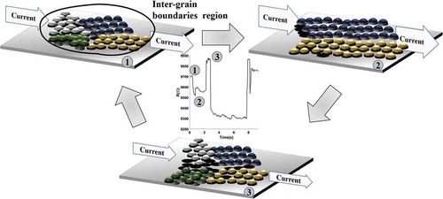
The formation of hot spots determines the local rearrangement of the crystalline phases and defect annealing, giving rise to either a further increase in the current (passage from sketch 1 to sketch 2) or to a junction break (passage from sketch 2 to sketch 3). The modification/breaking of the physical contacts among nanoparticles and the dynamical rearrangement of defects cause the observed resistive switching behavior [Citation43].
The basic phenomena that take place are Joule heating and electromigration phenomena. In a complex nanoscale junction (see and ), when a point contact between grain is smaller than the mean free path of electron, a small voltage drop (about 100 mV) can induce high temperature (up to thousands K) [Citation120] causing the re-arrangement of the junction through defect displacement, atom migration and re-crystallization [Citation64,Citation119,Citation120]. The mechanism schematically shown in is not confined to a single very small region: the local rearrangement of junctions affects the reorganization in the overall sample as discussed in more detail in ref. [Citation42], producing non-local effects [Citation121].
Starting from this picture one can understand the non-linear behavior and the presence of switching activity observed in continuous Au cluster-assembled films. Their structure is characterized by gaps acting as an effective barrier for the electron flow, thus involving non-ohmic conduction mechanism [Citation69] and bridges, where current can reach high density levels inducing breaking/formation events. This determines the global non-ohmic behavior observed with the application of low voltages (). The possibility to observe reversible switches controlled by the voltage pulse amplitude is due to the balance between connections formation and breaking taking place at the nanoscale for the different applied voltage values [Citation43].
To gain a deeper insight about the phenomena involved in the conduction process of cluster-assembled Au films and to discern among different mechanisms, the evolution of electrical conduction with temperature was investigated for films that underwent the switch activation [Citation44].
shows the temperature dependence of the current at different applied voltages normalized to the value measured at RT. A steep decrease of the current in the range between RT and 250 K; from 250 K to 24 K the decrease continues with a lower slope is observed.
In metallic systems, finite electrical resistivity arises due to scattering processes from impurities or various thermal excitations. The scattering events can be considered as statistically independent and thus additive, leading to the Matthiessen’s rule, where any thermally induced scattering simply increases the resistivity ρ(T) [Citation122,Citation123]. This corresponds to a positive Temperature Coefficient of Resistivity (TCR), i.e. dρ/dT > 0. clearly shows that cluster-assembled gold films are characterized by a trend of resistance with temperature typical of non-metallic systems.
Figure 18. Current normalized to the value measured at RT as function of temperature for different applied voltages of a cluster-assembled gold film. The sawtooth-like shape of curves at high voltages is due to switching events. From [Citation44]
![Figure 18. Current normalized to the value measured at RT as function of temperature for different applied voltages of a cluster-assembled gold film. The sawtooth-like shape of curves at high voltages is due to switching events. From [Citation44]](/cms/asset/e71df940-646a-45ad-afbd-65eac475c859/tapx_a_1908847_f0018_oc.jpg)
shows that cluster-assembled gold films have a negative TCR, in particular near RT, the oscillation around zero at lower temperatures can be ascribed to the presence of switching events of amplitude smaller than the resistance temperature variations.
Figure 19. (a) Temperature coefficient of resistivity (TCR) upon the application of a bias of 20 V for a cluster-assembled gold film. (b) Resistance of a cluster-assembled gold film as a function of the inverse of the temperature, both for cooling (square point) and heating (cross) cycles, in logarithmic scale. An Arrhenius-like trend is recognizable only for temperatures below 40 K. From [Citation44]
![Figure 19. (a) Temperature coefficient of resistivity (TCR) upon the application of a bias of 20 V for a cluster-assembled gold film. (b) Resistance of a cluster-assembled gold film as a function of the inverse of the temperature, both for cooling (square point) and heating (cross) cycles, in logarithmic scale. An Arrhenius-like trend is recognizable only for temperatures below 40 K. From [Citation44]](/cms/asset/e1b34822-e4d6-4e12-9985-833e751c9258/tapx_a_1908847_f0019_oc.jpg)
These results are unexpected for a nanostructured metallic film in the strong-coupling regime: only discontinuous gold ultrathin films and layers of molecularly linked gold nanoparticles have been reported to show non-metallic electrical conduction with temperature, although not in such a large temperature range. Self-assembled films of CnS2-linked Au nanoparticles have electrical properties ranging from insulating to metallic-like depending on the separation of the Au building blocks [Citation124]. In the insulating regime, electric transport occurs through cooperative electron tunneling (co-tunneling) at low temperatures, variable-range hopping (VRH) at intermediate temperatures, and Arrhenius-type behavior at high temperatures [Citation125]. The weight of each of these contributions depends on both the interparticle separation and the spatial organization.
Similarly, discontinuous films composed by irregularly shaped gold islands, assembled by atom deposition, with density close to the percolation threshold [Citation84,Citation126] show non-metallic transport strongly influenced by local disorder causing variations in the tunnel junction gaps and in the Coulomb blockade energies, due to island size fluctuations and offset charges [Citation95,Citation96]. A conduction percolation (co-percolation) model is applied to determine the total electrical current through the film as a function of both temperature and bias voltage [Citation95,Citation96]. The flowing of current is described as a percolation process through the ramified metallic islands. Unlike the case of hopping regime, in this case the high degree of disorder is related to the wide distribution, without mutual correlation, of the island electrostatic charging energy and of the parameters that characterize different tunnel junctions [Citation95,Citation96]. Increasing the island density till the reaching of strong-coupling regime, an ohmic electric transport is observed [Citation126].
Various types of disorder are considered as the origin of a negative TCR in ultrathin discontinuous films: I) variations in the tunnel gaps between adjacent islands; II) variations in the size and shape of the islands; III) random offset induced by trapped impurity charges in the substrate [Citation96,Citation122]. Cluster-assembled films are continuous and in the strong-coupling regime; however, they do not show the electrical behavior typical of continuous metallic films. This is probably due to the extremely high concentration of defects and grain boundaries slicing the crystal domains that constitute the films: upon deposition on the substrate, gold clusters formed in the gas phase do not lose their individuality and give rise to the multidomain structure, as confirmed by HRTEM analysis [Citation43,Citation44] ( and ). This kind of spatially extended disorder is substantially different from what is observed in polycrystalline metallic films grown by atom deposition, where the density of grain boundaries is much lower compared to that one finds in nanostructured systems [Citation44].
) displays the resistance vs the inverse of the temperature in logarithmic scale, showing that an Arrhenius-like behavior, characterized by a relation , is not detected except for temperatures below 40 K. The observed behavior deviates from a pure hopping conduction like that in the Efros-Shklovskii model [Citation127,Citation128] for discontinuous films. On the other hand, the co-percolation model successfully describes the non-Arrhenius behavior of the electrical resistance at low bias voltage [Citation95,Citation96], even if different mechanisms, such as Anderson localization, could contribute to the overall electrical behavior observed [Citation125].
) shows the I–V characteristics in the temperature range 295 K to 268 K. The trend is constantly linear in double logarithmic scale and unaffected by temperature change except for a higher resistance measured at lower temperatures. On the other hand, in the curves show steep slope variation for temperatures lower than 144 K. Although the trend slightly deviates from a pure power law, this agrees with the co-percolation model considering the occurrence of Coulomb blockade at cryogenic temperatures [Citation95,Citation116].
Figure 20. Current–voltage curves for a cluster-assembled gold film measured at different temperatures. (a) I–V curves for different temperatures in the range 295 K to 268 K. (b) I–V curves in the range 202 K to 24 K. From [Citation44]
![Figure 20. Current–voltage curves for a cluster-assembled gold film measured at different temperatures. (a) I–V curves for different temperatures in the range 295 K to 268 K. (b) I–V curves in the range 202 K to 24 K. From [Citation44]](/cms/asset/e5e6664a-80c3-4ddb-8c72-46996c198cbc/tapx_a_1908847_f0020_oc.jpg)
In order to provide further elements to highlight the role of the high density of grain boundaries and defect in determining the conduction regime, the behavior of films under constant bias in the time as been caharacterized. Since cluster-assembled gold films exhibit resistive switching (RS) phenomena [Citation42–44], the evolution of the RS activity with temperature can provide useful elements.
Figure 21. Resistive switching activity of a cluster-assembled gold film at 300 K and at 24 K. (a) The resistance-time graph, at 300 K (blue curve) and at 24 k (red one). (b) Distribution of the resistance values normalized by their average for the measurements carried out at constant voltage (5 V) at 300 K (red data) and at 24 K (blue data). From [Citation44]
![Figure 21. Resistive switching activity of a cluster-assembled gold film at 300 K and at 24 K. (a) The resistance-time graph, at 300 K (blue curve) and at 24 k (red one). (b) Distribution of the resistance values normalized by their average for the measurements carried out at constant voltage (5 V) at 300 K (red data) and at 24 K (blue data). From [Citation44]](/cms/asset/6a0a114e-e98a-4bee-a047-c690d24161de/tapx_a_1908847_f0021_oc.jpg)
- shows a typical resistance-time graph of the evolution of the resistance under 5 V bias (a) and the histogram () of the resistance, measured at both RT and 24 K upon the application of a constant voltage, for a duration of 300 s. The different peaks in the histogram are due to the different resistance levels explored during the resistive switching phenomena. A substantial RS activity at 24 K spanning a lower number of levels compared to that at RT is observed. This can be interpreted by considering that the flow of electric current causes the rearrangement of domains grown randomly with their related lattice defectivity and grain boundaries. As a consequence, concomitant dynamical creation and destruction of pathways with variable resistance occur through the rearrangement of defects [Citation43,Citation44]. This process is favored at RT by the high mobility of atoms and atomic planes [Citation129], while the latter is reduced at cryogenic temperatures.
The persistence of RS events at cryogenic temperatures could be related to the structure of cluster-assembled films characterized by a landscape crowded of defects and interconnects between grains resulting in an assembly of interacting nanojunctions [Citation41,Citation130]. Multiple conductance states are observed in single metallic nanojunctions at cryogenic temperatures [Citation131,Citation132] with electrical conductions characterized by discrete steps of conductance involving Coulomb blockade phenomena both in increasing and decreasing resistance [Citation131,Citation133]. Cluster-assembled gold films can be then considered as an assembly of nanojunctions connected in series and in parallel, thus displaying a collective electrical behavior resulting in resistive switching phenomena [Citation44]. This confirms the facts that high densities of grain boundaries and nanojunctions can significantly alter the electronic properties, favoring the onset of non-ohmic conduction mechanisms. Atomic rearrangement present under the application of high voltage bias contributes to the rearrangement of grain boundaries responsible for the switching events. The observed mechanism is substantially different from what observed in random networks of nanowires where ionic transport is involved [Citation109,Citation134,Citation135]. In this case, the highly correlated re-arrangement of grain boundaries changes the local conductivity as observed in single metallic nanowires [Citation136].
7. Summary and perspectives
In this review, we highlighted the electrical conduction features of nanogranular metallic thin films and the differences from the behavior of polycrystalline metallic films. These originate from the use of different building blocks: atoms in the case of polycrystalline films and clusters in the case of nanogranular thin films. The assembling of clusters has a profound influence on the structural and functional properties of the films: the number and the nature of defects in cluster-assembled metallic films are substantially different from those of polycrystalline films. This aspect has been recognized only very recently, suggesting that the extrapolation of an ohmic behavior for continuous cluster-assembled metallic systems, in analogy with the polycrystalline ones, could not be justified. As a matter of fact an increasing number of experimental observations show that cluster-assembled metallic films are characterized by a non-linear electric transport behavior and resistive switching phenomena. A thorough understanding of the fundamental mechanisms associated with the disorder in nanostructured systems is still lacking.
We hope that this review can stimulate the interest in pursuing a systematic characterization of the electrical transport properties of nanostructured metallic films in order to disclose the role played by the extremely high density of punctual and extended defects on the electron mobility. The observed departure from a metallic character in systems built with nanoscale metallic building blocks suggests the presence of very interesting physical effects taking place at the nano- and mesoscale.
From the technological point of view, nanogranular metallic systems have shown the presence of complex resistive switching phenomena that may be of interest in the field of devices for unconventional computing. Significant advances in the fundamental understanding of cluster-assembled metallic systems and in their exploitation will be assured by the development of robust and scalable fabrication technologies and by the availability of theoretical models able to describe electrical conduction phenomena at the nano- and mesoscale.
Conflict of interest
The authors declare no competing financial interests.
Acknowledgments
We thank Prof. A. Falqui and Dr. F. Borghi for insightful discussions and sharing of unpublished data.
Disclosure statement
No potential conflict of interest was reported by the authors.
Additional information
Funding
References
- Papadopoulos L, Porter MA, Daniels KE, et al. Network analysis of particles and grains. J Complex Networks. 2018;6:485.
- Jaeger HM, Nagel SR, Behringer RP. The physics of granular materials. Phys Today. 1996;49:32.
- De Gennes PG. Granular matter: a tentative view. Rev. Mod. Phys. 1999;71:S374.
- Yuan CN, Li YF, Sheng YJ, et al. Dry nanogranular materials. Appl. Phys. Lett. 2011;98(14):144102.
- Gleiter H. Nanocrystalline materials. Prog. Mater. Sci. 1989;33:223.
- Abeles B, Sheng P, Coutts MD, et al. Structural and electrical properties of granular metal films. Adv. Phys. 1975;24(3):407.
- Bursten JR, et al. Nano on reflection. Nat Nanotechnol. 2016;11:828.
- Jena P, Sun Q. Super atomic clusters: design rules and potential for building blocks of materials. Chem. Rev. 2018;118(11):5755.
- Tomalia DA, Khanna SN. A systematic framework and nanoperiodic concept for unifying nanoscience: hard/soft nanoelements, superatoms, meta-atoms, new emerging properties, periodic property patterns, and predictive Mendeleev-like nanoperiodic tables. Chem. Rev. 2016;116(4):2705.
- Luo Z, Castleman AW. Special and general superatoms. Acc. Chem. Res. 2014;47:2931.
- Benel C, Fischer A, Zimina A, et al. Controlling the structure and magnetic properties of cluster-assembled metallic glasses. Mater Horizons. 2019;6(4):727.
- Edelstein AS, Cammarata RC, editors. Nanomaterials: synthesis, properties, and applications. London: Institute of Physics; 1996.
- Tschopp MA, Murdoch HA, Kecskes LJ, et al. “Bulk” nanocrystalline metals: review of the current state of the art and future opportunities for copper and copper alloys. JOM. 2014;66(6):1000.
- Schiøtz J, Di Tolla FD, Jacobsen KW. Softening of nanocrystalline metals at very small grain sizes. Nature. 1998;391:561.
- Kumar KS, Van Swygenhoven H, Suresh S. Mechanical behavior of nanocrystalline metals and alloys11The golden jubilee issue—selected topics in materials science and engineering: past, present and future, edited by S. Suresh. Acta Mater. 2003;51(19):5743.
- Naik SN, Walley SM. The hall–petch and inverse hall–petch relations and the hardness of nanocrystalline metals. J. Mater. Sci. 2020;55(7):2661.
- Benel C, Reisinger T, Kruk R, et al. Cluster-assembled nanocomposites: functional properties by design. Adv. Mater. 2019;31(26):1806634.
- Faupel F, Zaporojtchenko V, Strunskus T, et al. Metal-polymer nanocomposites for functional applications. Adv. Eng. Mater. 2010;12:1177.
- Beloborodov IS, Lopatin AV, Vinokur VM, et al. Granular electronic systems. Rev. Mod. Phys. 2007;79(2):469.
- Ambrosetti G, Grimaldi C, Balberg I, et al. Solution of the tunneling-percolation problem in the nanocomposite regime. Phys. Rev. B - Condens. Matter Mater. Phys. 2010;81(15):1.
- Vinyas M, Athul SJ, Harursampath D, et al. A comprehensive review on analysis of nanocomposites: from manufacturing to properties characterization. Mater Res Express. 2019;6(9):092002.
- Homaeigohar S, Elbahri M. Switchable plasmonic nanocomposites. Adv. Opt. Mater. 2019;7:1801101.
- Milani P, Sowwan M, editors. Cluster beam deposition of functional nanomaterials and devices. Amsterdam: Elsevier; 2019.
- Huttel Y, editor. Gas-phase synthesis of nanoparticles. Weinheim: VCH; 2017.
- Milani P, Iannotta S. Cluster beam synthesis of nanostructured materials. In: Springer series in cluster physics Series Editor name: Prof. A. W. Castleman (Editor in Chief), Department of Chemistry , The Pennsylvania State University. Berlin: Springer; 1999.
- Benetti G, Caddeo C, Melis C, et al. Bottom-up mechanical nanometrology of granular Ag nanoparticles thin films. J Phys Chem C. 2017;121:22434.
- Piazzoni C, Buttery M, Hampson MR, et al. Tribological coatings for complex mechanical elements produced by supersonic cluster beam deposition of metal dichalcogenide nanoparticles. J. Phys. D. Appl. Phys. 2015;48(26):265302.
- Borghi F, Milani M, Bettini LG, et al. Quantitative characterization of the interfacial morphology and bulk porosity of nanoporous cluster-assembled carbon thin films. Appl. Surf. Sci. 2019;479:395.
- Borghi F, Sogne E, Lenardi C, et al. Cluster-assembled cubic zirconia films with tunable and stable nanoscale morphology against thermal annealing. J. Appl. Phys. 2016;120(5):055302.
- Goulas A, Van Ommen JR. Scalable production of nanostructured particles using atomic layer deposition. KONA Powder Part. J. 2014;31:234.
- Schulte C, Rodighiero S, Cappelluti MA, et al. Conversion of nanoscale topographical information of cluster-assembled zirconia surfaces into mechanotransductive events promotes neuronal differentiation. J Nanobiotechnology. (2016);14(1):1. .
- Borghi F, Podestà A, Piazzoni C, et al. Growth mechanism of cluster-assembled surfaces: from submonolayer to thin-film regime. Phys. Rev. Appl. 2018;9:044016.
- Bisio F, Palombo M, Prato M, et al. Optical properties of cluster-assembled nanoporous gold films. Phys. Rev. B - Condens. Matter Mater. Phys. 2009;80(20):205428.
- Jensen P. Growth of nanostructures by cluster deposition: experiments and simple models. Rev. Mod. Phys. 1999;71(5):1695.
- Sondheimer EH. The mean free path of electrons in metals. Adv. Phys. 1952;1:1.
- Mayadas AF, Shatzkes M. Electrical-resistivity model for polycrystalline films: the case of arbitrary reflection at external surfaces. Phys Rev B. 1970;1(4):1382.
- Kirkpatrick S. Percolation and conduction. Rev. Mod. Phys. 1973;54:574.
- Mukherjee A, Ankit K, Selzer M, et al. Electromigration-induced surface drift and slit propagation in polycrystalline interconnects: insights from phase-field simulations. Phys. Rev. Appl. 2018;9:44004.
- Balberg I, Azulay D, Toker D, et al. Percolation and tunneling in composite materials. Int J Mod Phys B. 2004;18:2091.
- Munoz RC, Arenas C. Size effects and charge transport in metals: quantum theory of the resistivity of nanometric metallic structures arising from electron scattering by grain boundaries and by rough surfaces. Appl. Phys. Rev. 2017;4:011102.
- Valencia D, Wilson E, Jiang Z, et al. Grain-boundary resistance in copper interconnects: from an atomistic model to a neural network. Phys. Rev. Appl. 2018;9(4):044005.
- Mirigliano M, Borghi F, Podestà A, et al. Non-ohmic behavior and resistive switching of Au cluster-assembled films beyond the percolation threshold. Nanoscale Adv. 2019;1(8):3119.
- Mirigliano M, Decastri D, Pullia A, et al. Complex electrical spiking activity in resistive switching nanostructured Au two-terminal devices. Nanotechnology. 2020;31(23):234001.
- Mirigliano M, Radice S, Falqui A, et al. Anomalous electrical conduction and negative temperature coefficient of resistance in nanostructured gold resistive switching films. Sci. Rep. 2020;10(1):1.
- Minnai C, Mirigliano M, Brown SA, et al. The nanocoherer: an electrically and mechanically resettableresistive switching device based on gold clusters assembled onpaper. Nano Futur. 2018;2:1.
- Minnai C, Bellacicca A, Brown SA, et al. Facile fabrication of complex networks of memristive devices. Sci. Rep. 2017;7(1):1.
- Haberland H, Insepov Z, Moseler M. Molecular-dynamics simulation of thin-film growth by energetic cluster impact. Phys Rev B. 1995;51(16):11061.
- Strobel R, Pratsinis SE. Flame aerosol synthesis of smart nanostructured materials. J. Mater. Chem. 2007;17(45):4743.
- Wegner K, Piseri P, Tafreshi HV, et al. Cluster beam deposition: a tool for nanoscale science and technology. J. Phys. D.: Appl. Phys. 2006;39:R439.
- Piseri P, Tafreshi HV, Milani P. Manipulation of nanoparticles in supersonic beams for the production of nanostructured materials. Curr. Opin. Solid State Mater. Sci. 2004;8:195.
- Palmer RE, Cai R, Vernieres J. Synthesis without solvents: the cluster (Nanoparticle) beam route to catalysts and sensors. Acc. Chem. Res. 2018;51(9):2296.
- Haberland H, Karrais M, Mall M, et al. Thin films from energetic cluster impact: a feasibility study. J Vac Sci Technol. 1992;10:3266. [ A Vacuum, Surfaces, Film].
- Kousal J, Shelemin A, Schwartzkopf M, et al. Magnetron-sputtered copper nanoparticles: lost in gas aggregation and found by in situ X-ray scattering. Nanoscale. 2018;10(38):18275. .
- Zanardi A, Bandiera D, Bertolini F, et al. Miniaturized FISH for screening of onco-hematological malignancies. Biotechniques. 2010;49(1):497.
- Santaniello T, Milani P. Cluster beam deposition of functional nanomaterials and devices. In: Elsevier. Vol. 15. 2020. p. 313, Paolo Milani, Mukhles Sowwan. Elsevier .
- Barborini E, Piseri P, Milani P. A pulsed microplasma source of high intensity supersonic carbon cluster beams. J. Phys. D. Appl. Phys. 1999;32(21):L105.
- Piseri P, Podestà A, Barborini E, et al. Production and characterization of highly intense and collimated cluster beams by inertial focusing in supersonic expansions. Rev. Sci. Instrum. 2001;72:2261.
- Tafreshi HV, Piseri P, Benedek G, et al. The role of gas dynamics in operation conditions of a pulsed microplasma cluster source for nanostructured thin films deposition. J. Nanosci. Nanotechnol. 2006;6:1140.
- Tafreshi HV, Benedek G, Piseri P, et al. A simple nozzle configuration for the production of low divergence supersonic cluster beam by aerodynamic focusing. Aerosol Sci. Technol. 2002;36(5):593.
- E Barborini, S Vinati, M Leccardi, P Repetto, G Bertolini, O Rorato, L Lorenzelli, M Decarli, V Guarnieri, C Ducatiand P Milani. Batch fabrication of metal oxide sensors on micro-hotplates. J. Micromech. Microeng. 2008;18:055015.
- Marelli M, Divitini G, Collini C, et al. Flexible and biocompatible microelectrode arrays fabricated by supersonic cluster beam deposition on SU-8. J. Micromech. Microeng. 2011;21(4):045013. .
- Reiss G, Vancea J, Hoffmann H. Grain-boundary resistance in polycrystalline metals. Phys. Rev. Lett. 1986;56:2100.
- Josell D, Brongersma SH, Tokei Z. Size-dependent resistivity in nanoscale interconnects. Annu. Rev. Mater. Res. 2009;39:231.
- Durkan C, Welland M. Size effects in the electrical resistivity of polycrystalline nanowires. Phys. Rev. B - Condens. Matter Mater. Phys. 2000;61(20):14215.
- Steinhögl W, Schindler G, Steinlesberger G, et al. Comprehensive study of the resistivity of copper wires with lateral dimensions of 100 nm and smaller. J. Appl. Phys. 2005;97:023706.
- Gall D. The search for the most conductive metal for narrow interconnect lines. J Appl Phys. 2020;127(5):050901.
- Petrov I, Barna PB, Hultman L, et al. Microstructural evolution during film growth. J Vac Sci Technol A. 2003;21(5):S117.
- Cattani M, Salvadori MC. contribution of the morphological grain sizes to the electrical resistivity of platinum and gold thin films. Surf. Rev. Lett. 2004;11:463.
- Zhigal’skii GP, Jones BK. The physical properties of thin metal films. London: Taylor & Francis; 2003.
- Abadias G, Simonot L, Colin JJ, et al. Volmer-Weber growth stages of polycrystalline metal films probed by in situ and real-time optical diagnostics. Appl. Phys. Lett. 2015;107(18):183105.
- Messier R, Giri AP, Roy RA. Revised structure zone model for thin film physical structure. J Vac Sci Technol A. 1984;2(2):500.
- Sarakinos K. A review on morphological evolution of thin metal films on weakly-interacting substrates. Thin Solid Films. 2019;688:137312.
- Barna PB, Adamik M. Fundamental structure forming phenomena of polycrystalline films and the structure zone models. Thin Solid Films. 1998;317:27.
- Ekinci KL, Valles JM. Formation of polycrystalline structure in metallic films in the early stages of Zone I growth. Acta Mater. 1998;46:4549.
- Camacho JM, Oliva AI. Surface and grain boundary contributions in the electrical resistivity of metallic nanofilms. Thin Solid Films. 2006;515:1881.
- Yamamuro S, Sumiyama K, Hihara T, et al. Geometrical and electrical percolation in nanometre-sized Co-cluster assemblies. J Phys Condens Matter. 1999;11(16):3247.
- Barborini E, Corbelli G, Bertolini G, et al. The influence of nanoscale morphology on the resistivity of cluster-assembled nanostructured metallic thin films. New J. Phys. 2010;12:073001.
- Bouwen W, Kunnen E, Temst K, et al. Characterization of granular Ag films grown by low-energy cluster beam deposition. Thin Solid Films. 1999;354(1–2):87.
- Pauwels B, Van Tendeloo G, Bouwen W, et al. Low-energy-deposited Au clusters investigated by high-resolution electron microscopy and molecular dynamics simulations. Phys. Rev. B - Condens. Matter Mater. Phys. 2000;62:10383.
- Bardotti L, Prével B, Treilleux M, et al. Deposition of preformed gold clusters on HOPG and gold substrates: influence of the substrate on the thin film morphology. Appl. Surf. Sci. 2000;164:52.
- Fuchs G, Montadon C, Treilleux M, et al. Low-energy Bi cluster beam deposition. J. Phys. D. Appl. Phys. 1993;26:1114.
- Schmelzer J, Brown SA, Wurl A, et al. Finite-size effects in the conductivity of cluster assembled nanostructures. Phys. Rev. Lett. 2002;88:226802.
- Dunbar ADF, Partridge JG, Schulze M, et al. Morphological differences between Bi, Ag and Sb nano-particles and how they affect the percolation of current through nano-particle networks. Eur Phys J D. 2006;39:415.
- Sattar A, Fostner S, Brown SA. Quantized conductance and switching in percolating nanoparticle films. Phys. Rev. Lett. 2013;111:136808.
- Yoon B, Akulin VM, Cahuzac P, et al. Morphology control of the supported islands grown from soft-landed clusters. Surf. Sci. 1999;443(1–2):76.
- Mélinon P, Fuchs G, Cabaud B, et al. Low-energy cluster beam deposition: do you need it?. J Phys I. 1993;3:1585.
- Borghi F, Mirigliano M, Milani P, et al. Toward a science campus in Milan. 2018. p. 67. Gewerbestrasse.
- Podestà A, Borghi F, Indrieri M, et al. Nanomanufacturing of titania interfaces with controlled structural and functional properties by supersonic cluster beam deposition. J. Appl. Phys. 2015;118:234309.
- Bardotti L, Prével B, Mélinon P, et al. Deposition of AuN clusters on Au(111) surfaces. II. Experimental results and comparison with simulations. Phys. Rev. B - Condens. Matter Mater. Phys. 2000;62(4):2835.
- Me P, Pre B, Hou Q, et al. Deposition of Au N clusters on Au(111) surfaces. I. Atomic-scale modeling. Phys Rev B. 2000;62:2825.
- Stauffer D, Aharony A. Introduction to percolation theory. London: Taylor & Francis; 2003.
- Balberg I. Tunnelling and percolation in lattices and the continuum. J. Phys. D. Appl. Phys. 2009;42(6):064003.
- Saberi AA. Recent advances in percolation theory and its applications. Phys Rep. 2015;578:1.
- Maaroof AI, Evans BL. Onset of electrical conduction in Pt and Ni films. J. Appl. Phys. 1994;76:1047.
- Yajadda MMA, Müller KH, Ostrikov K. Effect of Coulomb blockade, gold resistance, and thermal expansion on the electrical resistance of ultrathin gold films. Phys Rev B. 2011;84:235431.
- Muller KH, Yajadda MA. Electron transport in discontinuous gold films and the effect of Coulomb blockade and percolation. J. Appl. Phys. 2012;111(12):123705.
- Fuchs K. The conductivity of thin metallic films according to the electron theory of metals. Math. Proc. Cambridge Philos. Soc. 1937;34(1):100.
- Lutzer B, Bethge O, Zimmermann C, et al. J Vac Sci Technol B Nanotechnol Microelectron Mater Process Meas Phenom. In situ resistance measurements during physical vapor deposition of ultrathin metal films on Si(111) at room temperature. 2017;35:051802.
- Borziak PG, Kulyupin SA, Nepuko SA, et al. Electrical conductivity and electron emission from discontinuous metal films of homogeneous structure. Thin Solid Films. 1981;76(4):359.
- Vancea J, Hoffmann H, Kastner K. Mean free path and effective density of conduction electrons in polycrystalline metal films. Thin Solid Films. 1984;121:201.
- Namba Y. Resistivity and temperature coefficient of thin metal films with rough surface. Jpn. J. Appl. Phys. 1970;9:1326.
- Vancea J, Reiss G, Hoffmann H. Mean-free-path concept in polycrystalline metals. Low-temperature resistance and its temperature dependence in nanostructured silver. Phys Rev B. 1987;35(12):6435.
- Qin XY, Zhang W, Zhang LD, et al. Phys Rev B. 1997;56:596.
- Arnason SB, Herschfield SP, Hebard AF. Bad metals made with good-metal components. Phys. Rev. Lett. 1998;81:3936.
- Mooij JH. Electrical conduction in concentrated disordered transition metal alloys. Phys Status Solidi. 1973;17(2):521.
- Anderson PW, Abrahams E, Ramakrishnan TV. Possible explanation of nonlinear conductivity in thin-film metal wires. Phys. Rev. Lett. 1979;43:718.
- Last BJ, Thouless DJ. Percolation theory and electrical conductivity. Phys. Rev. Lett. 1971;27(25):1719.
- Melinon P, Jensen P, Hu JX, et al. Comparison of molecular and cluster deposition: evidence of different percolation processes. Phys Rev B. 1991;44(22):12562.
- Mallinson JB, Shirai S, Acharya SK, et al. Avalanches and criticality in self-organized nanoscale networks. Sci. Adv. 2019;5:1.
- Fostner S, Brown SA. Neuromorphic behavior in percolating nanoparticle films. Phys Rev E. 2015;92(5):052134.
- Barabási A-L, Stanley HE. Fractal concepts in surface growth. Cambridge: CAMBRIDGE University Press; 1995.
- Nasiri N, Elmøe TD, Liu Y, et al. Self-assembly dynamics and accumulation mechanisms of ultra-fine nanoparticles. Nanoscale. 2015;7(21):9859.
- Andersson T. The electrical properties of ultrathin gold films during and after their growth on glass. J. Phys. D. Appl. Phys. 1976;9:973.
- Acha C. Graphical analysis of current-voltage characteristics in memristive interfaces. J. Appl. Phys. 2017;121:134502.
- Burr T, Seraphin A, Werwa E, et al. Carrier transport in thin films of silicon nanoparticles. Phys. Rev. B - Condens. Matter Mater. Phys. 1997;56(8):4818.
- Chen W, Ahmed H, Nakazoto K. Coulomb blockade at 77 K in nanoscale metallic islands in a lateral nanostructure. Appl. Phys. Lett. 1995;66(24):3383.
- Aguilar M, Oliva AI, Quintana P. The effect of electrical current (DC) on gold thin films. Surf. Sci. 1998;409:501.
- Bo R, Nasiri N, Chen H, et al. Low-voltage high-performance UV photodetectors: an interplay between grain boundaries and Debye length. ACS Appl Mater Interfaces. 2017;9(3):2606.
- Durkan C, Welland ME, Welland ME. Analysis of failure mechanisms in electrically stressed Au nanowires. J Appl Phys. 1999;86(3):1280.
- Halbritter A, Csonka S, Kolesnychenko OY, et al. Connective neck evolution and conductance steps in hot point contacts. Physical Review B. 2002;65(4):454131.
- Milano G, Pedretti G, Fretto M, et al. Brain-inspired structural plasticity through reweighting and rewiring in multi-terminal self-organizing memristive nanowire networks. Anomalous electrical conduction and negative temperature coefficient of resistance in nanostructured gold resistive switching films. Adv. Intell. Syst. 2020;2(8):2000096.
- Ciuchi S, Di Sante D, Dobrosavljević V, et al. Disordered electronic systems. npj Quantum Mater. 2018;3:1.
- Lee PA, Ramakrishnan TV. Rev Mod Phys. 1985;57:287.
- Zabet-khosousi A, Trudeau P, Suganuma Y, et al. Metal to insulator transition in films of molecularly linked gold nanoparticles. Phys. Rev. Lett. 2006;96(15):156403.
- Jiang C-W, Ni I-C, Tzeng S-D, et al. Anderson localization in strongly coupled gold-nanoparticle assemblies near the metal–insulator transition. Appl. Phys. Lett. 2012;101:083105.
- Yajadda MMA, Levchenko I, Ostrikov K. Gold nanoresistors with near-constant resistivity in the cryogenic-to-room temperature range. Appl. Phys. Lett. 2011;110(2):023303.
- Shklovskii BI, Éfros AL. Percolation theory and conductivity of strongly inhomogeneous media. Uspekhi Fiz. Nauk. 1975;117:401.
- Efros AL, Shklovskii BI. Critical behaviour of conductivity and dielectric constant near the metal-non-metal transition threshold. Phys Status Solidi. 1976;76:475.
- Bose SK, Shirai S, Mallinson JB, et al. Synaptic dynamics in complex self-assembled nanoparticle networks. Faraday Discuss. 2019;213:471.
- Bowman M, Anaya A, Korotkov AL, et al. Localization and capacitance fluctuations in disordered Au nanojunctions. Phys Rev B. 2004;69:205405.
- Hoffman-Vogel R. Electromigration and the structure of metallic nanocontacts. Appl. Phys. Rev. 2017;4:031302.
- Kim T, Zhang X, Nicholson DM, et al. Large discrete resistance jump at grain boundary in copper Nanowire. Nano Lett. 2010;10(8):3096.
- Anaya A, Korotkov AL, Bowman M, et al. Nanometer-scale metallic grains connected with atomic-scale conductors. J Appl Phys. 2003;93(6):3501.
- Manning HG, Niosi F, Da Rocha CG, et al. Emergence of winner-takes-all connectivity paths in random nanowire networks. Nat. Commun. (2018);9:1.
- Nirmalraj PN, Bellew AT, Bell AP, et al. Manipulating connectivity and electrical conductivity in metallic nanowire networks. Nano Lett. 2012;12:5966.
- Johnson SL, Sundararajan A, Hunley DP, et al. Memristive switching of single-component metallic nanowires. Nanotechnology. 2010;21(12):125204.