
Abstract
A new technique of diamond and InGaP room temperature bonding in atmospheric air is reported. Diamond substrate cleaned with H2SO4/H2O2 mixture solution is bonded to InGaP exposed after removing the GaAs layer by the H2SO4/H2O2/H2O mixture solution. The bonding interface is free from interfacial voids and mechanical cracks. An atomic intermixing layer with a thickness of about 8 nm is formed at the bonding interface, which is composed of C, In, Ga, P, and O atoms. After annealing at 400 °C, no exfoliation occurred along the bonding interface. An increase of about 2 nm in the thickness of the atomic intermixing layer is observed, which plays a role in alleviating the thermal stress caused by the difference of the thermal expansion coefficient between diamond and InGaP. The bonding interface demonstrates high thermal stability to device fabrication processes. This bonding method has a large potential for bonding large diameter diamond and semiconductor materials.
1. Introduction
The heat generated in the electronic devices by self-heating during operation will greatly increase with rapidly developing of the high integration, miniaturization, and high performance of the electronic devices. The heat will result in an increase in the device temperature that will significantly degrade the reliability and performance of the devices. The main factor limiting the device heat dissipation is attributed to the low-thermal conductivity semiconductor substrate. Because the heat is mainly spread out through the semiconductor substrate, therefore, the most effective way is to replace the low-thermal conductivity substrate with a high-thermal conductivity substrate.
Diamond is attracting a wide attention as a heat spreader because of its critically high thermal conductivity of 18–22 W/cm K, which is one of the most potential materials for suppressing the rise in the device temperature [Citation1,Citation2]. A low-defect epitaxial growth of diamond on semiconductor substrates such as Si, GaN, Ga2O3 is difficult because of the large mismatch in the lattice constants and thermal expansion coefficients of diamond and the semiconductor substrates. GaN-on-diamond structures are being extensively studied by depositing an intermediate layer such as SiN on the backside of GaN and then depositing diamond [Citation3–6]. However, the crystal quality of the deposited diamond is very low, which largely lowers the thermal conductivity. As an alternative technique, the wafer bonding technique allows materials with different lattice constants and thermal expansion coefficients to be seamless bonded.
The room temperature bonding of diamond and Si, and SiC using an Au intermediate layer by atomic diffusion bonding and surface-activated bonding (SAB) methods has been reported [Citation7,Citation8]. However, the bonding interface with a metal layer is unsuitable for high-frequency device applications because the metal layer has a very low resistivity such that a large parasitic capacitance will be induced. The room temperature bonding of diamond and GaN using a silicon amorphous layer by SAB method has been demonstrated [Citation9,Citation10]. In addition, the room temperature direct bonding of diamond and Si using the SAB method has also been reported [Citation11,Citation12]. In SAB, the substrate surfaces are activated by Ar fast-atom beam irradiation under ultra-high vacuum conditions, and then the activated surfaces are contacted together by applying pressure. Although this method enables the bonding interface a high-bonding strength without heating, the ultra-high vacuum less than 1 × 10⁻⁵ Pa and the high-flatness substrate with an average roughness lower than 1 nm are required. Recently, the hydrophilic bonding of diamond cleaned by the NH3/H2O2 mixture solution and SiO2 formed on Si activated by oxygen plasma under vacuum has been reported [Citation13]. However, it is difficult to apply to device fabrication because the diamond/SiO2 bonding interface cannot withstand the annealing temperature required for the device fabrication process. For the bonding of diamond and semiconductor materials, it is the most ideal to bond in atmospheric air at room temperature without using vacuum equipment. It is of the most important that the bonding interface can withstand the device fabrication process. It is necessary to activate the surface of the bonding substrate in the bonding process of dissimilar materials. Therefore, if the substrate surface can be activated by chemicals, the substrate can be directly bonded at room temperature in atmospheric air. InGaP with lattice matched to GaAs has been extensively applied to high-power and high-frequency devices. InGaP or GaAs can be easily removed with selective chemicals so that the activated surface is exposed.
In this work, we explore a new technique for the room temperature bonding of diamond and InGaP in atmospheric air. The chemical bonding state and the surface morphology of the bonding material surfaces were characterized by X-ray photoelectron spectroscopy (XPS) and atomic force microscope (AFM). The structures and the atomic diffusion of the 400 °C-annealed interface are investigated by transmission electron microscopy (TEM) and energy-dispersive X-ray spectroscopy (EDX).
2. Experimental
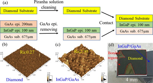
Here, we demonstrate the direct bonding of diamond and GaAs/InGaP, which has the self-heating problem leading to the deterioration of device performance and reliability [Citation14,Citation15]. High-pressure and high-temperature synthetic Ib type (100) single-crystal diamond substrate and GaAs/InGaP epitaxial layer grown on GaAs substrate were used for the bonding experiments. The GaAs/InGaP epitaxial substrate was composed of a 200-nm-thick GaAs layer and a 100-nm-thick InGaP layer grown on GaAs (100) substrate. Before bonding, the diamond was cleaned by an H2SO4/H2O2 mixture solution at 80 °C for 10 min, the mixture ratio of H2SO4 and H2O2 was 4: 1. After cleaning, the diamond was rinsed with deionized water for 3 min, then dried by an N2 flow. The GaAs/InGaP epitaxial substrate was cleaned by an acetone and isopropyl alcohol in an ultrasonic bath for 300 s, dried under N2 flow. After cleaning, the GaAs layer was removed by a mixture solution composed of H2SO4, H2O2, and H2O, the mixture ratio of H2SO4: H2O2: H2O was fixed to 1: 10: 100, then rinsed with deionized water for 1 min and dried by an N2 flow. A schematic of the bonding process is shown in . After removing the GaAs layer, the diamond substrate was directly placed onto the InGaP/GaAs substrate in atmospheric air, and then lightly pressed with a tweezer. The room temperature bonding of diamond and InGaP/GaAs was formed in atmospheric air.
Figure 1. (a) Schematic of the room temperature bonding process of diamond and InGaP. (b,c) AFM images of the diamond and the InGaP surface, respectively. (c) Optical microscope image of the diamond/InGaP bonded sample surface.
The effect of annealing temperature on the bonding interface structure was investigated. The annealing process was conducted in an ambient N2 gas for 1 min at 400 °C with a heating rate of 60 °C/min after removing the GaAs substrate. After annealing, the temperature was naturally cooled. The chemical bonding state of the diamond and the InGaP/GaAs substrate surfaces was evaluated by XPS (ESCA-3400) with a monochromatic Mg Kα X-ray radiation source. The surface roughness of the diamond and the InGaP/GaAs substrates was evaluated by AFM (SPM-9600). The microstructure and chemical composition analysis of the bonding interface were performed using TEM (JEM-2200FS) equipped with an EDS apparatus. The TEM samples were fabricated using the focused ion beam (FIB) technique at room temperature (Helios NanoLab600i; Thermo Fisher Scientific).
3. Results and discussion
AFM images of the diamond and the InGaP surfaces are shown in , respectively. The average roughness (Ra) values of the diamond and the InGaP surfaces were determined to be 0.27 and 2.93 nm, respectively, by AFM. The InGaP surface was found to be very rough; the Ra value was ten times larger than that of the diamond. Obviously, the InGaP with a rough surface is not suitable for room temperature bonding. The optical microscope image of the bonded sample surface is shown in . Some fringe patterns with a small area due to the unbonded region were observed at the contacting surface. However, no fringe pattern was observed in an about 85% contact area of diamond and InGaP, which indicated that the room temperature bonding of diamond and InGaP was achieved in atmospheric air at room temperature. After removing the GaAs substrate, an approximately 10% peeling of the bonded area was observed around the unbonded region due to the weak bonding strength. Furthermore, no significant reduction of the bonded area was observed in the 400 °C bonded sample.
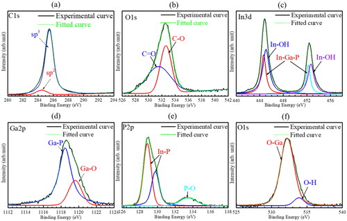
The C1s and O1s spectra of diamond surface are shown in , and , respectively. The spectra were fitted by a Gaussion function after subtracting the background using Shirley’s method. The C1s and O1s spectra were both decomposed into two components located at 284.5 and 285.5 eV, and 531.5 and 532.6 eV, which correspond to sp2 and sp3 bonded carbons, and C = O and C‒O bonding states, respectively [Citation16,Citation17]. As shown in , the In3d spectrum of InGaP surface was decomposed into four peaks located at 444.7, 445.1, 452.2, and 452.7 eV, which are associated with In‒Ga‒P and In‒OH bonding states, respectively [Citation18]. The Ga2p spectrum of InGaP is shown in . The two peaks located at 1118.5 and 1119.6 eV decomposed from the Ga2p spectrum are assigned to Ga‒P and Ga‒O chemical bonding states, respectively. The P2p spectrum was divided into three peaks located at 128.8, 129.8, and 133.5 eV (), which are contributed to P‒In and P‒O chemical bonding states, respectively. As shown in , the O1s spectrum of InGaP was decomposed into two peaks located at 532.3 and 533.9 eV, which are associated with O-Ga and O-H bonding states, respectively.
Figure 2. (a) C1s and (b) O1s spectra of diamond, (c) In3d, (d) Ga2p, (e) P2p, and (f) O1s spectra of InGaP.
shows a low-magnification cross-sectional TEM image, a high-resolution TEM (HRTEM) image taken from along the InGaP [001] direction, and an HRTEM image taken along the diamond [001] direction of the bonding interface before annealing, respectively. A thin layer between diamond and InGaP at the center of the TEM image as shown in was observed, which is contributed to the bonding interface. No unbonded micro-voids and mechanical cracks were observed at the bonding interface, which indicates that the direct bonding of diamond and InGaP in the micro-level was obtained. As shown in , we found that an intermediate layer with a thickness of about 8 nm was formed at the bonding interface and the intermediate layer was very uneven in thickness as shown in . EDX mappings of the bonding interface before annealing are shown in . To compare the EDX mappings of the bonding interface, it is evident that there is an oxide layer formed at the bonding interface. The X-ray intensity profiles of C, Ga, P, In, and O atoms near the bonding interface before annealing are shown in . A small peak of O atom was observed at the bonding interface because the bonding process was conducted in atmospheric air. The intensity gradients of C, Ga, P, and In atoms were observed, which indicated that there was an atomic intermixing layer formed at the bonding interface. In addition, it should be noted that a small peak of In atom at the diamond side of the bonding interface was observed. However, In atoms were depleted at the InGaP side of the bonding interface.
Figure 3. (a) Low-magnification cross-sectional TEM image, (b) HRTEM image taken along the InGaP [001] direction, (c) HRTEM image taken along the diamond [001] direction, (d) EDS mappings, and (e) X-ray intensity profiles of C, P, In, Ga, and O elements of the bonding interface before annealing.
![Figure 3. (a) Low-magnification cross-sectional TEM image, (b) HRTEM image taken along the InGaP [001] direction, (c) HRTEM image taken along the diamond [001] direction, (d) EDS mappings, and (e) X-ray intensity profiles of C, P, In, Ga, and O elements of the bonding interface before annealing.](/cms/asset/60a4185a-9bbe-432e-9ff6-0c2ca1d9a8f4/tfdi_a_1869435_f0003_c.jpg)
A low-magnification cross-sectional TEM image, an HRTEM image taken from along the InGaP [001] direction, an HRTEM image taken from along the diamond [001] direction of the bonding interface after annealing at 400 °C are shown in , respectively. After annealing at 400 °C, interfacial spalling and cracks caused by the difference in thermal expansion coefficient were not observed at the interface, which indicated that the bonding interface has excellent thermal stability. Like the bonding interface before annealing, an intermediate layer was also observed at the interface after annealing at 400 °C, as shown in . The thickness of the intermediate layer was determined to be about 10 nm, which is thicker than that of the bonding interface before annealing. Moreover, the intermediate layer is more uniform in thickness. shows the EDX mappings of the bonding interface after annealing at 400 °C. A high-intensity layer of the In and O atoms was observed at the interface. Furthermore, a transition layer of C atoms was also observed at the interface. X-ray intensity profiles of C, Ga, P, In, and O atoms at the bonding interface after annealing at 400 °C are shown in . The intensity peak positions of In and O atoms shifted to the InGaP side were observed. It was found that the peak intensity of In atoms was increased after annealing. However, the densities of Ga and P atoms were depleted at the interface after annealing at 400 °C. The depletion part of Ga and P atoms was replaced with the C atoms increase.
Figure 4. (a) Low-magnification cross-sectional TEM image, (b) HRTEM image taken along the InGaP [001] direction, (c) HRTEM image taken along the diamond [001] direction, (d) EDS mappings, and (e) X-ray intensity profiles of C, P, In, Ga, and O elements of the bonding interface after annealing at 400 °C.
![Figure 4. (a) Low-magnification cross-sectional TEM image, (b) HRTEM image taken along the InGaP [001] direction, (c) HRTEM image taken along the diamond [001] direction, (d) EDS mappings, and (e) X-ray intensity profiles of C, P, In, Ga, and O elements of the bonding interface after annealing at 400 °C.](/cms/asset/e3e0326c-2cf0-4d9e-bb30-71644c941fec/tfdi_a_1869435_f0004_c.jpg)
On the basis of the experimental results, we found that the intermediate layer formed at the bonding interface was composed of C, In, Ga, P, and O atoms; the ununiform of the intermediate layer in the thickness was attributed to the morphology of the InGaP surface due to rough surface (). For the room temperature direct bonding, the surface roughness of bonding materials is a very important factor. The Ra value of bonding material surface smaller than 1 nm was necessary for achieving the direct bonding of diamond and semiconductor substrates [Citation11,Citation13]. Although the Ra value (2.93 nm) of the InGaP surface was larger than 1 nm, the direct bonding of diamond and InGaP was achieved. The main reason was due to the chemical reaction occurred between the oxide layer formed on InGaP and the C = O and C-O chemical bonds formed on the diamond after contacting. The oxide layer should originate from the In-OH, Ga-O, P-O, O-Ga, and O-H chemical bonds formed on InGaP, as shown in . Since there is no alloy composed of C, Ga, In, and P atoms, it is difficult to find a long-distance mutual diffusion at the interface. Moreover, there is not a stable phase composed of the In-OH, Ga-O, P-O, O-Ga, O-H, C = O, and C-O chemical bonds. Therefore, each element at the interface should move after annealing. The increased amorphous layer thickness should be associated with the oxygen atoms moving. In fact, the oxygen intensity peak is moving to the InGaP side as shown in . On the other hand, the rich In atom layer formed at the diamond side of the bonding interface should also play an important role in the direct bonding of diamond and InGaP. It has been reported that the direct bonding of Si wafer using an indium tin oxide layer at low temperatures was achieved [Citation19]. In addition, wafer bonding using a thin indium film at 140 °C has also been reported [Citation20].
The thermal expansion coefficient (5.4 × 10⁻⁶/K at 300 K) of InGaP is several times higher than that of diamond (2.3 × 10⁻⁶/K at 300 K). However, no interfacial spalling and mechanical cracks were observed at the 400 °C-annealed interface. In addition, no exfoliation of the InGaP layer bonded to diamond was observed in the 400 °C-annealed sample. The thickness of the InGaP layer bonded to diamond may be too thin so that the thermal stress caused by the thermal expansion coefficient mismatch was too small to induce the InGaP layer cracks or the spalling. These results imply that the bonding interface with thermal stability of 400 °C should be related to the atomic intermixing layer formed at the bonding interface. No lattice fringes were observed in the atomic intermixing layer even changing electron beam incident direction during TEM observation, which indicated that the atomic intermixing layer is an amorphous layer. The amorphous layer should play a role in relieving stress caused by the difference in thermal expansion coefficient between diamond and InGaP. A similar result has been reported for the diamond/Si interface fabricated by SAB [Citation21]. After annealing at 400 °C, the increased amorphous layer thickness is more helpful in the relaxation of the stress. The amorphous layer thickness increase is unlike the heterointerfaces fabricated by SAB, in which the amorphous layer thickness decreased with increasing annealing temperature due to the recrystallization of the amorphous layer [Citation22–26]. The main difference is no oxygen atoms detected in the SAB-fabricated interface because the bonding processes were conducted in the extremely high-level vacuum condition. The amorphous layer thickness increased should be correlated with the diffusion of O atoms toward the InGaP. The O atom diffusion destroyed the crystal structure of InGaP and made it form amorphous.
The amorphous layer formed at the bonding interface should affect the thermal boundary conductance. It has been reported that the thermal boundary conductance of the GaN/SiC interface with an amorphous layer was 1.35 times larger than that of the interface without amorphous layer [Citation27]. Because the amorphous layer has lower thermal conductivity than the bulk materials, the increase of the amorphous layer thickness also has impact on the thermal boundary conductance. As reported, the thermal conductivity of the amorphous layer decreases by 70% when the thickness increases from 2 nm to 1000 nm [Citation28]. Obviously, the decrease in the thermal conductivity of the amorphous layer formed at the diamond/InGaP interface due to the amorphous layer thickness increasing in several nanometers can be ignored. In addition, the thermal boundary conductance of the Ga2O3/SiC interface with a 10 nm Al2O3 interlayer was 30% lower in comparison with that of the interface with a 30 nm Al2O3 interlayer, as reported in a previous study [Citation29]. Consequently, although the amorphous layer has a certain effect on the thermal boundary conductance, the intrinsic thermal boundary conductance of the diamond/InGaP interface is the main factor to affect the heat dissipation properties of InGaP-on-diamond devices.
It is difficult to evaluate the bonding strength by the conventional tensile test due to the small diamond substrate size. Therefore, a simple bond strength test was conducted, when a load was applied to the GaAs cross-section of the bonded sample, no peeling of the bonding interface was observed until the GaAs fractured. This simple test indicated that the bonding interface has the mechanical strength higher than that of bulk GaAs. In addition, the TEM samples were fabricated on the InGaP layer bonded to the diamond after removing GaAs substrate by mechanical polishing and selective wet etching methods. No large area exfoliation of the bonding interface was observed during GaAs removing processes, which indicated that the bonding interface has excellent mechanical strength and chemical stability. Furthermore, the bonding interface can withstand the annealing process required for the ohmic formation of Si and GaAs semiconductors. Most important of all, the direct bonding of diamond and InGaP can be performed in atmospheric air at room temperature. This technique does not require expensive experimental equipment, but only require simple treatment of the bonding material surface with chemicals. In addition, it is possible to bond semiconductors with a rough surface. Therefore, this method is very suitable for the direct bonding of diamond and semiconductors with a large area. However, whether it can be applied to other materials is unclear, it is necessary to further investigate.
4. Conclusion
We have demonstrated a new technique for the room temperature bonding of diamond and InGaP in atmospheric air. Although the InGaP surface has a Ra value of 2.93 nm, no interfacial voids and cracks were observed at the diamond/InGaP bonding interface. An atomic intermixing layer composed of C, In, Ga, P, and O atoms was formed at the bonding interface. The intermixing layer thickness was obtained to be about 8 nm, which was increased to 10 nm after the bonding interface annealed at 400 °C. No interfacial exfoliation or mechanical cracks resulting from the thermal expansion coefficient mismatch between diamond and InGaP were observed at the bonding interface. The bonding interface demonstrated excellent thermal stability for the device fabrication process. These results suggest that this bonding method could be applied to the large-diameter wafer bonding of diamond and semiconductor materials.
Disclosure statement
No potential conflict of interest was reported by the authors.
Additional information
Notes on contributors
Jianbo Liang
Dr. Jianbo Liang is working in Department of Physical Electronics and Informatics at Osaka City University as an associate professor. His research is currently engaged in the direct bonding of various material at room temperature for realizing advanced electronics devices and the devices characterization.
Yuji Nakamura
Mr. Yuji Nakamura will receive the B. Eng. Degree in Applied Physics and Electronics form Osaka City University.
Yutaka Ohno
Dr. Yutaka Ohno is working in the Institute for Materials Research, Tohoku University, as an associate professor (http:// http://www-lab.imr.tohoku.ac.jp/∼yutakaohno/). A focus is on quantitative analyses of the impurity segregation ability of grain boundaries in Si and compounds by APT combined with STEM and ab-initio calculations, but also on the study of atomistic structures of semiconductor nanostructures by optical measurements (cathodoluminescence, micro-photoluminescence, near-field optical measurements) under TEM.
Yasuo Shimizu
Dr. Yasuo Shimizu is working at National Institute for Materials Science (Japan) as a special researcher. His research is focused on dopant behavior analysis in Si and Ge-based semiconductor materials and nanostructures by using atom probe tomography combined with a site-specific focused ion beam technique. The present work was carried out at the Oarai Center, Institute for Materials Research, Tohoku University (Japan).
Yasuyoshi Nagai
Dr. Yasuyoshi Nagai is working in the Institute for Materials Research, Tohoku University, as a professor. A focus is to analyze fine defects, their clusters, and impurity segregation and clustering, by using atom probe tomography, TEM and positron annihilation spectroscopy etc.
Hongxing Wang
Dr. Hongxing Wang is working in School of Electronic and Information Engineering at Xian Jiaotong University as a professor. His research is focused on diamond crystal growth, diamond based electronic devices fabrication, and their characterization.
Naoteru Shigekawa
Dr. Naoteru Shigekawa is working at Osaka City University as a professor. A focus is on the fabrication of hetero-interfaces and advanced hybrid semiconductor devices such as multijunction solar cells and heterojunction bipolar transistors using surface activated bonding and their characterization.
References
- Yamamoto Y, Imai T, Tanabe K, et al. The measurement of thermal properties of diamond. Diamond Relat Mater. 1997; 6(8): 1057–1061.
- Nosaeva K, Weimann N, Rudolph M, et al. Erratum: Improved thermal management of InP transistors in transferred-substrate technology with diamond heat-spreading layer. Electron Lett. 2015; 51(13): 1010–1012.
- Cho J, Francis D, Altman D, et al. Phonon conduction in GaN-diamond composite substrate. J Appl Phys. 2017; 121(5): 055105.
- Käding OW, Rösler M, Zachai R, et al. Lateral thermal diffusivity of epitaxial diamond films. Diamond Relat Mater. 1994; 3(9): 1178–1182.
- Sun H, Pomeroy J, Simon R, et al. Temperature-dependent thermal resistance of GaN-on-diamond HEMT wafers. IEEE Electron Device Lett. 2016; 37(5): 621–624.
- Zhou Y, Anaya J, Pomeroy J, et al. Barrier-layer optimization for enhanced GaN-on-diamond device cooling. ACS Appl Mater Interfaces. 2017; 9(39): 34416–34422.
- Matsumae T, Kurashima Y, Umezawa Y, et al. Room-temperature bonding of single-crystal diamond and Si using Au/Au atomic diffusion bonding in atmospheric air. Microelectron Eng. 2018; 195: 68–73.
- Minoura Y, Ohki T, Okamoto N, et al. Surface activated bonding of SiC/diamond for thermal management of high-output power GaN HEMTs. Jpn J Appl Phys. 2020; 59 (Suppl G): SGGD03.
- Mu F, He R, Suga T. Room temperature GaN-diamond bonding for high-power GaN-on-diamond devices. Scr Mater. 2018; 150: 148–151.
- Cheng Z, Mu F, Yates L, et al. Interfacial thermal conductance across room-temperature-bonded GaN/diamond interfaces for GaN-on-diamond devices. ACS Appl Mater Interfaces. 2020; 12(7): 8376–8384.
- Liang J, Masuya S, Kasu M, et al. Realization of direct bonding of single crystal diamond and Si substrates. Appl Phys Lett. 2017; 110(11): 111603.
- Liang J, Masuya S, Kim S, et al. Stability of diamond/Si bonding interface during device fabrication process. Appl Phys Express. 2019; 12(1): 016501.
- Matsumae T, Kurashima Y, Umezawa H, et al. Hydrophilic direct bonding of diamond (111) substrate using treatment with H2SO4/H2O2. Jpn J Appl Phys. 2020; 59 (Suppl B): SBBA01.
- Choi S, Peake GM, Keeler GA, et al. Thermal design and characterization of heterogeneously integrated InGaP/GaAs HBTs. IEEE Trans Compon Packag Manuf Technol. 2016; 6(5): 740–748.
- Pierściński K, Pierścińska D, Iwińska M, et al. Investigation of thermal properties of mid-infrared AlGaAs/GaAs quantum cascade lasers. J Appl Phys. 2012; 112(4): 043112.
- Humbert B, Hellala N, Ehrhardt JJ, et al. X-ray photoelectron and Raman studies of microwave plasma assisted chemical vapour deposition (PACVD) diamond films. Appl Surf Sci. 2008; 254(20): 6400–6409.
- Wang C, Huang N, Zhuang H, et al. Photochemical functionalization of diamond films using a short carbon chain acid. Chem Phys Lett. 2016; 646: 87–90.
- López-Escalante MC, Gabás M, García I, et al. Differences between GaAs/GaInP and GaAs/AlInP interfaces grown by movpe revealed b depth profiling and angle-resolved X-ray photoelectron spectroscopies. Appl Surf Sci. 2016; 360: 477–484.
- Hönle M, Oberhumer P, Hingerl K, et al. Mechanism of indium thin oxide//indium tin oxide direct wafer bonding. Thin Solid Films. 2020; 704: 137964.
- Straessle R, Pétremand Y, Briand D, et al. Evaluation of thin film indium bonding at wafer level. Procedia Eng. 2011; 25: 1493–1496.
- Liang J, Zhou Y, Masuya S, et al. Annealing effect of surface-activated bonded diamond/Si interface. Diamond Relat Mater. 2019; 93: 187–192.
- Liang J, Nishida S, Arai M, et al. Effects of thermal annealing process on the electrical properties of p+-Si/n-SiC heterojunctions. Appl Phys Lett. 2014; 104(16): 161604.
- Howlader MMR, Zhang F. Void-free strong bonding of surface activated silicon wafers from room temperature to annealing at 600 °C. Thin Solid Film. 2010; 519(2): 804–808.
- Liang J, Ohno Y, Yamashita Y, et al. Characterization of nanoscopic Cu/diamond interfaces prepared by surface-activated bonding: implications for thermal management. ACS Appl Nano Mater. 2020; 3(3): 2455–2462.
- Takagi H, Maeda R, Hosoda N, et al. Transmission electron microscope observations of Si/Si interface bonded at room temperature by Ar beam surface activation. Jpn J Appl Phys. 1999; 38 (Part 1, No. 3A): 1589–1594.
- Takagi H, Kikuchi K, Maeda R, et al. Surface activated boding of silicon wafers at room temperature. Appl Phys Lett. 1996; 68(16): 2222–2224.
- Mu F, Cheng Z, Shi J, et al. High thermal boundary conductance across bonded heterogeneous GaN-SiC interfaces. ACS Appl Mater Interfaces. 2019; 11(36): 33428–33434.
- Al Mohtar A, Tessier G, Ritasalo R, et al. Thickness-dependent thermal properties of amorphous insulating thin films measured by photoreflectance microscopy. Thin Solid Films. 2017; 642: 157–162.
- Cheng Z, Mu F, You T, et al. Thermal transport across ion-cut monocrystalline β-Ga2O3 thin films and bonded β-Ga2O3–SiC interfaces. ACS Appl Mater Interfaces. 2020; 12(40): 44943–44951.