
Abstract
We report the tailoring of the electrical properties of mechanically exfoliated multilayer (ML) molybdenum disulfide (MoS2) by chemical doping. Electrical charge transport and Raman spectroscopy measurements revealed that the p-toluene sulfonic acid (PTSA) imposes n-doping in ML MoS2. The shift of threshold voltage for ML MoS2 transistor was analyzed as a function of reaction time. The threshold voltage shifted toward more negative gate voltages with increasing reaction time, which indicates an n-type doping effect. The shift of the Raman peak positions was also analyzed as a function of reaction time. PTSA treatment improved the field-effect mobility by a factor of ~4 without degrading the electrical characteristics of MoS2 devices.
1. Introduction
Over the last several years, two-dimensional (2D) semiconducting transition-metal dichalcogenide (TMD) has attracted increased research attention because of its emerging electrical and optical properties and great potential in practical applications [Citation1, Citation2]. Graphene is a representative 2D material that has a conical Dirac spectrum of energy states without a band gap, which results in many interesting physical properties as well as stimulating applications [Citation3–Citation6]. However, the gapless band structure of graphene makes it unsuitable as an electronic material in logic circuits. Molybdenum disulfide (MoS2), a layered TMD, has emerged as a feasible alternative to graphene because it has a moderate energy gap with mechanical flexibility, chemical and thermal stability, and absence of dangling bonds [Citation7–Citation14]. A layer of MoS2 consists of a molybdenum monolayer sandwiched between two sulfur monolayers. The strong intralayer bonds and weak interlayer van der Waals forces make it possible to exfoliate individual MoS2 layers. MoS2 crystals can also be obtained in a large scale by chemical exfoliation and chemical vapor deposition (CVD) techniques [Citation15].
MoS2-based electronic and optoelectronic devices such as field-effect transistors (FETs), integrated circuits, solar cells, photodetectors, memory devices, chemical and biosensors, supercapacitors, and photocatalyzed hydrogen evolution reactors have been successfully fabricated [Citation10, Citation14–Citation17]. FET is a basic and important application of semiconducting TMD materials. Several issues, including reducing the contact resistance, using different substrates, and depositing high-k materials as the top gate, have been focused on to improve the performance of MoS2 FET [Citation18–Citation22]. Given the ultrathin structure of MoS2 layers, doping of this material has yet to be fully developed. Traditional methods of doping such as ion implantation are not suitable for MoS2 thin layer; hence, alternative approaches, such as chemical and molecular doping, must be explored.
Chemical doping has been used to investigate the surface charge transfer between dopant molecules and MoS2 layer [Citation23]. The charge transfer between dopant and host material modulates the Fermi level and results in the modification of the optical and electrical properties of 2D materials. Chemical doping of MoS2 nanoflakes with solution-based dopants, gases, metal nanoparticles, or self-assembled monolayers has already been reported [Citation24–Citation28]. Mouri et al reported the tunable photoluminescence of monolayer MoS2 flakes by n-type and p-type dopants in chemical solution [Citation25]. Fang et al reported a degenerate n-doping of MoS2 by potassium metal ions and the significant change in the electron density of MoS2 nanoflakes [Citation26]. Gold nanoparticles were used by Shi et al to effectively decorate MoS2 layers via wet chemical method [Citation27]. They found that gold nanoparticles impose p-doping to the MoS2 transistors. Li et al studied the carrier doping of MoS2 nanoflakes by functional self-assembled monolayers with different dipole moments [Citation28]. Our group also demonstrated ultraviolet light-induced reversible and stable charge carrier modulation in single-layer, bilayer and multilayer (ML) MoS2 nanosheets with a combination of N2 and O2 gases [Citation29].
Here, we report the tailoring of the electronic properties of ML MoS2 by p-toluene sulfonic acid (PTSA) molecular doping. PTSA is a well-known dopant for conducting polymers and is highly soluble in water. The charge transport measurements and Raman spectroscopy revealed that PTSA molecule imposes n-doping in ML MoS2. The threshold voltages shifted toward more negative gate voltages after exposure of PTSA molecules for different periods of time, revealing the n-doping in ML MoS2. The charge carrier density and field-effect mobility were also estimated and found to be significantly improved after PTSA treatment. Results indicate that chemical modification is a simple approach to tailor the electrical properties of few-layered MoS2 while maintaining its important electrical characteristics.
2. Experimental details
2.1. Sample preparation
ML MoS2 film was mechanically exfoliated from bulk crystals of molybdenite (SPI Supplies, USA) by the scotch tape method and then transferred to a 300 nm thick highly p-doped SiO2/Si substrate. Optical microscopy, Raman spectroscopy, and atomic force microscopy (AFM) aided in identifying the number of layers of the MoS2 flakes. The ML MoS2 had seven to eight monolayers. Raman spectra were obtained with a Renishaw microspectrometer with 514 nm laser wavelength at room temperature. The laser power was kept at ≈1.0 mW to avoid local heating and defect introduction by the laser.
2.2. Device fabrication and measurements
Photolithography technique was used to make large patterned electrodes (Cr/Au of 6/30 nm thicknesss) for ML MoS2 devices. As the final process, Cr/Au (10/80 nm) ohmic contacts were patterned by e-beam lithography. The channel length of transistors was kept almost same (~2.8 μm) for all devices. The devices were annealed in a tube furnace at 200 °C in a flow of 100 sccm Ar and 10 sccm H2 for 4 h to remove lithography resist residue and minimize the contact resistance of the devices. Electrical characterizations of the devices were performed using Keithley 2400 and Picometer 6485 instruments by two-probe measurements at room temperature in vacuum.
2.3. PTSA doping and characterizations
Electrical charge transport measurements and Raman spectroscopy were used to characterize the pristine ML MoS2 film. The same device was then doped with PTSA for different periods of time, and the effect of PTSA doping was investigated by charge transport measurements and Raman spectroscopy. The PTSA monohydrate (ACS reagent, ≥ 98.5%, Aldrich) was dissolved in deionized water to make a PTSA solution with 0.1 M concentration. The ML MoS2 film on the Si/SiO2 substrate was soaked in the PTSA solution for certain periods of time and blow-dried by nitrogen. The sample was then placed in a vacuum desiccator for 1 d to completely dry. The procedure described in our previous papers was followed [Citation30, Citation31].
3. Results and discussion
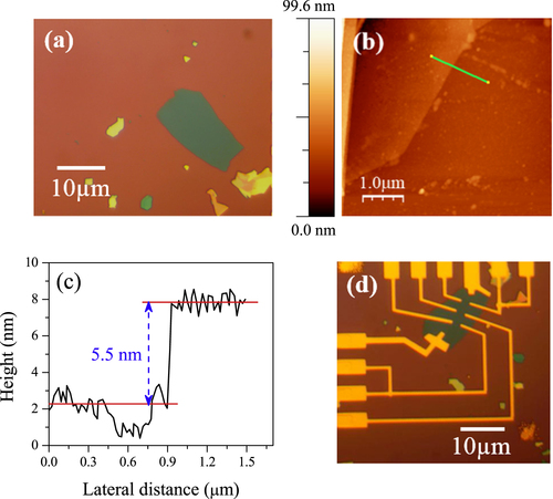
Figure (a) shows the optical image of ML MoS2 on SiO2 substrate. The fabrication process started with the micromechanical exfoliation of naturally occurring crystals of molybdenite using scotch tape method. The ML MoS2 flakes were then transferred to a 300 nm thick SiO2 substrate with underlying highly p-doped silicon. ML MoS2 was first identified by the contrast in an optical microscope. ML MoS2 was further characterized by Raman spectroscopy and AFM. Figures (b) and (c) show the surface morphology and corresponding height profile of the ML MoS2 film using AFM. The thickness of MoS2 is approximately 5.5 nm, which indicates seven to eight layers of MoS2. Figure (d) represents the optical image of the ML MoS2 film with Cr/Au electrical contacts. The thickness of the Cr/Au electrical contact is 6 nm/80 nm.
Figure 1. (a) The optical image of mechanically exfoliated ML MoS2 on Si/SiO2 substrate. (b) AFM image of ML MoS2. (c) Height profile measured along the green line in panel (b). (d) Optical image of fabricated device with source and drain electrodes of the transistors made of Cr/Au (6/80 nm).
Tailoring the electronic properties of semiconducting channel materials is essential for using these materials in high-performance electronic and optoelectronic devices. Several approaches have been applied to modulate the electronic properties of 2D nanomaterials by depositing dopant atoms, chemical modification by absorption of gas molecules/aromatic compounds, and by surface-induced interstitial doping [Citation32]. In general, interstitial doping is usually difficult to control and often introduces defects, thereby reducing the mobility of host materials. Chemical modification, especially non-covalent functionalization, is one of the most effective methods to tailor the electrical properties of 2D nanomaterials. This type of chemical modification does not change the basic electronic structure and preserves the desired electronic properties of 2D nanomaterials by minimizing the damage to the lattice. In our previous reports, the electronic properties of exfoliated single-layer, bilayer and tri-layer graphene, as well as CVD-grown single-layer graphene, were tailored by PTSA molecular doping without degrading its transparency and electrical properties [Citation30, Citation31].
Figure (a) shows the Raman spectra of ML MoS2 before and after PTSA modification for different periods of time. Two characteristic peaks, E12g (in-plane vibration) and A1g (out-of-plane vibration), appear around 384 and 408 cm–1, respectively. The frequency difference between these two Raman modes varies depending on the number of layers and can be easily used as a thickness indicator. The frequency difference between the Raman A1g and E12g modes (Δ = A1g − E12g) is approximately 24 cm–1, indicating few layers. The Raman spectra of ML MoS2 after PTSA treatment shows downward shifting of the E12g and A1g peak positions compared with pristine ML MoS2, as shown in figure (a). The downward shifting of the E12g and A1g peak positions is attributed to the n-doping of MoS2 as previously reported by others for different systems [Citation33, Citation34]. The shifting of the E12g and A1g peaks toward low wave numbers increases with increasing PTSA exposure time. The n-doping of ML MoS2 is also confirmed by the electrical charge transport measurements.
Figure 2. (a) The Raman spectra of ML MoS2 with 514 nm laser source at room temperature before and after PTSA treatment for different exposure times. (b) Drain–source current as a function of back gate voltage (Vg) for ML MoS2 before and after PTSA treatment for different exposure times.
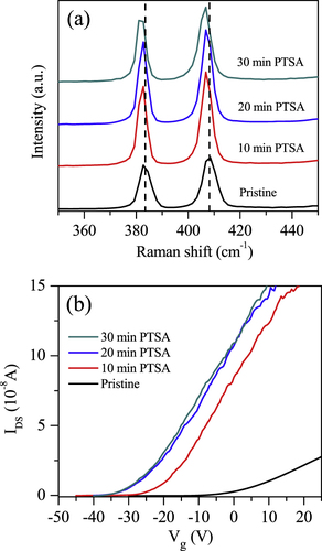
Figure (b) displays the drain current IDS as a function of the applied back-gate voltage Vg at a fixed drain–source voltage, VDS = 10 mV, for pristine and PTSA-doped ML MoS2. All electrical characterizations of the devices were performed at room temperature in a vacuum chamber. The IDS–Vg graph reveals an n-type channel for ML MoS2. The IDS shifts toward negative Vg after PTSA treatment. The shift toward the negative gate voltage increases with increasing PTSA exposure time, as shown in figure (b). Shifting of the threshold voltage toward the negative gate voltage reveals the n-doping in the ML MoS2 layers. The same trend is observed on the other devices.
Figure (a) illustrates the threshold voltage as a function of PTSA exposure time. The threshold voltage shifts toward the negative gate voltage as the PTSA reaction time increases, revealing the n-doping in MoS2. This chemical doping turns out to be very stable and the same characteristics of the PTSA doped devices have been observed after 10 days in the ambient atmosphere.
Figure 3. (a) Threshold voltage as a function of the PTSA exposure time of ML MoS2. (b) Charge carrier density at Vg = 0 V and field-effect mobility as a function of the PTSA exposure time of ML MoS2.
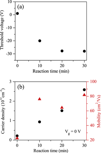
Figure (b) shows the field-effect mobility of ML MoS2 as a function PTSA reaction time. The mobility of the samples was determined using the relation where L is the channel length, W is the channel width,
is the slope of the transfer characteristic of the device in the linear region for particular doping time, and VDS = 0.01 V. The length and width of the fabricated device are 2.8 and 9.7 μm, respectively. The gate capacitance Cg for Si/SiO2 is ∼115 aF μm−2. The mobility of pristine ML MoS2 was measured as 22.4 cm2 V−1 s−1. The mobility remarkably improved after PTSA treatment, and it was found to be 84 cm2 V−1 s−1 after 30 min of exposure to PTSA molecules. The improvement in mobility may be due to reduction of Schottky barrier height between source/drain and MoS2 layers. PTSA increases the electron density in MoS2 channel, which changes the Fermi level of MoS2 and lowers the Schottky barrier height between the electrode and MoS2. Figure (b) also shows the charge carrier density (n) of ML MoS2 as a function of PTSA exposure time at Vg = 0 V. Figure (b) clearly shows that the charge carrier density of ML MoS2 significantly changed after different periods of PTSA treatment. The charge carrier densities of our ML MoS2 transistors were estimated using the relation
where e is the elementary charge and VT is the corresponding threshold voltage of the device at different PTSA exposure times.
The n-type doping effect by PTSA solution can be understood as follows. Mo is electropositive in nature as it belongs to 4th transition group of periodic table. The valence electronic configuration of Mo (5S14d5) shows a capacity to accept electrons. On the other hand, has three oxygen atoms, in which two are doubly bonded and the third one is singly bonded with S atom, so there is a resonance in the [O = S–O] bond.
can coordinate via monodentate and bidentate moieties owing to the presence of resonance in its structure. The aromatic ring of PTSA contains two groups (CH3 and SO3), and
is more reactive than
coordinates with Mo through bidentate mode and shifts electrons to s and d-orbitals of Mo. By accepting the electrons, Mo becomes electron rich and causes n-doping.
4. Conclusions
A simple technique to modulate the electronic properties of ML MoS2 by PTSA molecular doping was demonstrated. The effect of PTSA doping on the electric properties of ML MoS2 was investigated by Raman spectroscopy and charge transport measurements. The charge transport and Raman spectroscopy measurements revealed that PTSA molecules impose n-doping in ML MoS2. The threshold voltage shifted toward more negative gate voltages, thereby confirming n-doping in ML MoS2. The shift of the Raman peak frequencies was also analyzed as a function of reaction time. Our study demonstrated that molecular n-doping using PTSA is a feasible scheme for improving the electronic properties of MoS2-based devices.
Acknowledgments
This research was supported by Nano-Material Technology Development Program (2012M3A7B4049888) through the National Research Foundation of Korea (NRF) funded by the Ministry of Science, ICT and Future Planning. This research was also supported by Priority Research Center Program (2010-0020207) and the Basic Science Research Program (2013R1A1A2061396) through NRF funded by the Ministry of Education.
References
- LeeCYanHBrusL EHeinzT FHoneJRyuS 2010 Anomalous lattice vibrations of single- and few-layer MoS2 ACS Nano 4 2695 2700 2695–700 10.1021/nn1003937
- RadisavljevicBRadenovicABrivioJGiacomettiVKisA 2011 Single-layer MoS2 transistors Nat. Nanotechnol. 6 147 150 147–50 10.1038/nnano.2010.279
- NovoselovK SGeimA KMorozovS VJiangDKatsnelsonM IGrigorievaI VDubonosS VFirsovA A 2005 Two-dimensional gas of massless Dirac fermions in graphene Nature 438 197 200 197–200 10.1038/nature04233
- SchwierzF 2010 Graphene transistors Nat. Nanotechnol. 5 487 496 487–96 10.1038/nnano.2010.89
- LiaoLLinY CBaoMChengRBaiJLiuYQuYWangK LHuangYDuanX 2010 High-speed graphene transistors with a self-aligned nanowire gate Nature 467 305 308 305–8 10.1038/nature09405
- LinY M 2011 Wafer-scale graphene integrated circuit Science 332 1294 1297 1294–7 10.1126/science.1204428
- XiaFMuellerTLinY MValdes-GarciaAAvourisP 2009 Ultrafast graphene photodetector Nat. Nanotechnol. 4 839 843 839–43 10.1038/nnano.2009.292
- MakK FLeeCHoneJShanJHeinzT F 2010 Atomically thin MoS(2): a new direct-gap semiconductor Phys. Rev. Lett. 105 136805 10.1103/PhysRevLett.105.136805
- SplendianiASunLZhangYLiTKimJChimC YGalliGWangF 2010 Emerging photoluminescence in monolayer MoS2 Nano Lett. 10 1271 1275 1271–5 10.1021/nl903868w
- GhatakSPalA NGhoshA 2011 Nature of electronic states in atomically thin MoS(2) field-effect transistors ACS Nano 5 7707 7712 7707–12 10.1021/nn202852j
- LiuHYeP D D 2012 MoS2 dual-gate MOSFET with atomic-layer-deposited Al2O3 as top-gate dielectric IEEE Electr. Device Lett. 33 546 548 546–8 10.1109/LED.2012.2184520
- LiuHGuJ JYeP D 2012 MoS2 nanoribbon transistors: transition from depletion mode to enhancement mode by channel-width trimming IEEE Electr. Device Lett. 33 1273 1275 1273–5 10.1109/LED.2012.2202630
- JariwalaDSangwanV KLateD JJohnsJ EDravidV PMarksT JLauhonL JHersamM C 2013 Band-like transport in high mobility unencapsulated single-layer MoS2 transistors Appl. Phys. Lett. 102 173107 10.1063/1.4803920
- LiuHSiMNajmaeiSNealA TDuYAjayanP MLouJYeP D 2013 Statistical study of deep submicron dual-gated field-effect transistors on monolayer chemical vapor deposition molybdenum disulfide films Nano Lett. 13 2640 2646 2640–6 10.1021/nl400778q
- WangHYuL LLeeY HShiY MHsuAChinM LLiL JDubeyMKongJPalaciosT 2012 Integrated circuits based on bilayer MoS2 transistors Nano Lett. 12 4674 4680 4674–80 10.1021/nl302015v
- YuTLimBXiaY 2010 Aqueous-phase synthesis of single-crystal ceria nanosheets Angew. Chem. 49 4484 4487 4484–7 10.1002/anie.201001521
- MatteH SGomathiAMannaA KLateD JDattaRPatiS KRaoC N 2010 MoS2 and WS2 analogues of graphene Angew. Chem. 49 4059 4062 4059–62 10.1002/anie.201000009
- LateD JLiuBMatteH SDravidV PRaoC N 2012 Hysteresis in single-layer MoS2 field effect transistors ACS Nano 6 5635 5641 5635–41 10.1021/nn301572c
- WangQ HKalantar-ZadehKKisAColemanJ NStranoM S 2012 Electronics and optoelectronics of two-dimensional transition metal dichalcogenides Nat. Nanotechnol. 7 699 712 699–712 10.1038/nnano.2012.193
- BertolazziSKrasnozhonDKisA 2013 Nonvolatile memory cells based on MoS2/graphene heterostructures ACS Nano 7 3246 3252 3246–52 10.1021/nn3059136
- LateD J 2013 Sensing behavior of atomically thin-layered MoS2 transistors ACS Nano 7 4879 4891 4879–91 10.1021/nn400026u
- DhakalK PDuongD LLeeJNamHKimMKanMLeeY HKimJ 2014 Confocal absorption spectral imaging of MoS2: optical transitions depending on the atomic thickness of intrinsic and chemically doped MoS2 Nanoscale 6 13028 13035 13028–35 10.1039/C4NR03703K
- ChoiM SQuDLeeDLiuXWatanabeKTaniguchiTYooW J 2014 Lateral MoS2 p–n junction formed by chemical doping for use in high-performance optoelectronics ACS Nano 8 9332 9340 9332–40 10.1021/nn503284n
- KimS 2012 High-mobility and low-power thin-film transistors based on multilayer MoS2 crystals Nat. Commun. 3 1011 10.1038/ncomms2018
- MouriSMiyauchiYMatsudaK 2013 Tunable photoluminescence of monolayer MoS2 via chemical doping Nano Lett. 13 5944 5948 5944–8 10.1021/nl403036h
- FangHTosunMSeolGChangT CTakeiKGuoJJaveyA 2013 Degenerate n-doping of few-layer transition metal dichalcogenides by potassium Nano Lett. 13 1991 1995 1991–5 10.1021/nl400044m
- ShiYHuangJ KJinLHsuY TYuS FLiL JYangH Y 2013 Selective decoration of Au nanoparticles on monolayer MoS2 single crystals Sci. Rep. 3 1839 10.1038/srep01839
- LiYXuC YHuPZhenL 2013 Carrier control of MoS2 nanoflakes by functional self-assembled monolayers ACS Nano 7 7795 7804 7795–804 10.1021/nn402682j
- SinghA KAndleebSSinghJDungH TSeoYEomJ 2014 Ultraviolet-light-induced reversible and stable carrier modulation in MoS2 field-effect transistors Adv. Funct. Mater. 24 7125 7132 7125–32
- SinghA KAhmadMSinghV KShinKSeoYEomJ 2013 Tailoring the electrical properties of graphene layers by molecular doping ACS Appl. Mater. Interfaces 5 5276 5281 5276–81 10.1021/am401119j
- SinghA KIqbalM WSinghV KIqbalM ZLeeJ HChunS HShinKEomJ 2012 Molecular n-doping of chemical vapor deposition grown graphene J. Mater. Chem. 22 15168 15174 15168–74 10.1039/c2jm32716c
- HanS W 2011 Band-gap transition induced by interlayer van der Waals interaction in MoS2 Phys. Rev. B 84 045409 10.1103/PhysRevB.84.045409
- KiriyaDTosunMZhaoPKangJ SJaveyA 2014 Air-stable surface charge transfer doping of MoS(2) by benzyl viologen J. Am. Chem. Soc. 136 7853 7856 7853–6 10.1021/ja5033327
- YuL 2014 Graphene/MoS2 hybrid technology for large-scale two-dimensional electronics Nano Lett. 14 3055 3063 3055–63 10.1021/nl404795z