
Figures & data
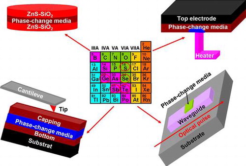
Figure 1. An example of memory taxonomy.
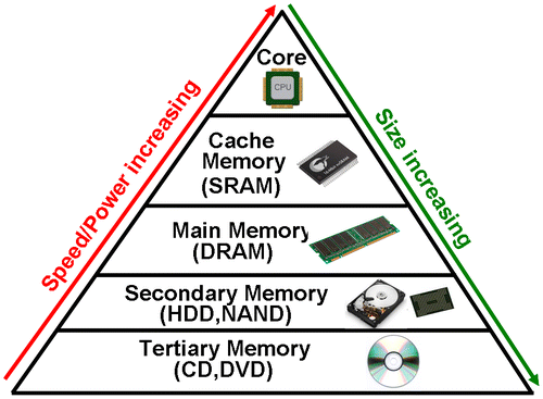
Figure 2. A modified memory taxonomy for the age of ‘big data’.
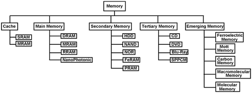
Figure 3. Typical elements in the chalcogenide family used for memory.
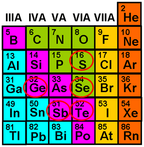
Figure 4. Tertiary Ge-Sb-Te phase diagram with some popular chalcogenide alloys highlighted.
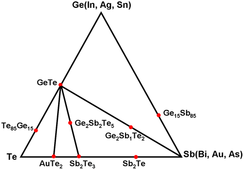
Figure 5. Crystallization kinetics of (a) nucleation-dominate and (b) growth-dominant materials.
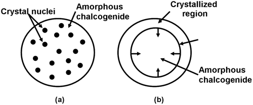
Figure 6. Crystallization and amorphization processes along with the temporal evolution of temperature.
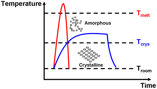
Figure 7. ‘Threshold switching’ phenomenon.
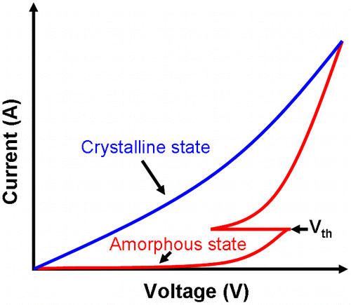
Figure 8. Measured resistance as a function of time for different annealing temperatures TA, under conditions TR = TA (a) and TR = 30°C (b). Note the different temperature behaviour of the curve slope, indicating the power-law exponent ν of resistance drift. Reprinted with permission from [Citation64].
![Figure 8. Measured resistance as a function of time for different annealing temperatures TA, under conditions TR = TA (a) and TR = 30°C (b). Note the different temperature behaviour of the curve slope, indicating the power-law exponent ν of resistance drift. Reprinted with permission from [Citation64].](/cms/asset/fe266729-68b1-45ef-a847-08f142b00920/tsta_a_1332455_f0008_oc.gif)
Figure 9. Optical near-field storage system.
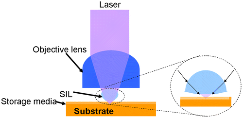
Figure 10. The ‘Millipede’ system when operated in its write and readout modes. Upgraded and reprinted with permission from [Citation106].
![Figure 10. The ‘Millipede’ system when operated in its write and readout modes. Upgraded and reprinted with permission from [Citation106].](/cms/asset/263d6abf-caea-49a4-9c59-f3d9f0b45c9d/tsta_a_1332455_f0010_oc.gif)
Figure 11. Phase-change probe memory when operated in (a) write mode, and (b) read mode. Reprinted with permission from [Citation17].
![Figure 11. Phase-change probe memory when operated in (a) write mode, and (b) read mode. Reprinted with permission from [Citation17].](/cms/asset/dfa0f04d-501d-4004-8e3a-1e57a7d345ef/tsta_a_1332455_f0011_oc.gif)
Figure 12. The typical architecture of SPPCM.
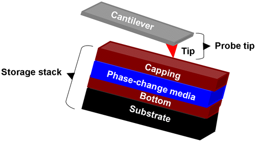
Figure 13. The designed optimized storage stack for SPPCM.
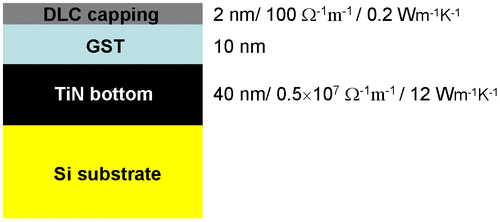
Figure 14. (a) Schematic of the ‘encapsulated’ tip concept, and (b) the experimentally fabricated encapsulated tip. Upgraded and reprinted with permission from [Citation124].
![Figure 14. (a) Schematic of the ‘encapsulated’ tip concept, and (b) the experimentally fabricated encapsulated tip. Upgraded and reprinted with permission from [Citation124].](/cms/asset/85eade69-bec0-47e7-8187-19f088af526e/tsta_a_1332455_f0014_oc.gif)
Figure 15. The resulting crystalline bit from the designed optimal electrical probe memory. The written bit exhibits a radius of approximately 5 nm, corresponding to 10 Tbit/in2. Reprinted with permission from [Citation130].
![Figure 15. The resulting crystalline bit from the designed optimal electrical probe memory. The written bit exhibits a radius of approximately 5 nm, corresponding to 10 Tbit/in2. Reprinted with permission from [Citation130].](/cms/asset/82cf354f-472c-4cf2-87ab-cb9b76d49e0c/tsta_a_1332455_f0015_oc.gif)
Figure 16. Schematic (top) of conventional mark-position recording, as used in probe memories to date; schematic (middle) of a new mark-length recording strategy; and (bottom) a current image of mark-length recorded bits in a phase-change medium (image is 580 nm × 140 nm and recorded bit sequence is 11001110111101110001111000111 with a bit cell length of 20 nm). Reprinted with permission from [Citation131].
![Figure 16. Schematic (top) of conventional mark-position recording, as used in probe memories to date; schematic (middle) of a new mark-length recording strategy; and (bottom) a current image of mark-length recorded bits in a phase-change medium (image is 580 nm × 140 nm and recorded bit sequence is 11001110111101110001111000111 with a bit cell length of 20 nm). Reprinted with permission from [Citation131].](/cms/asset/19300522-4129-4524-ad94-67e4d04bf828/tsta_a_1332455_f0016_oc.gif)
Figure 17. (a) Front view and (b) top view of SPPCM based on patterned PCMs.
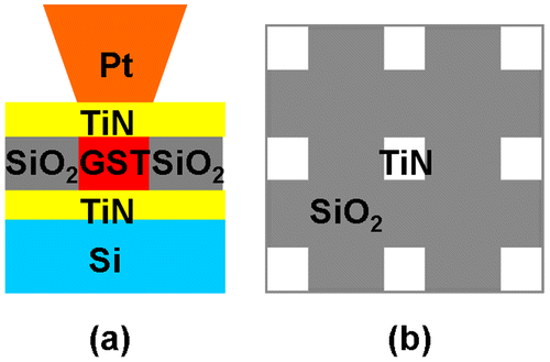
Figure 18. The cell structure of the OUM PRAM.
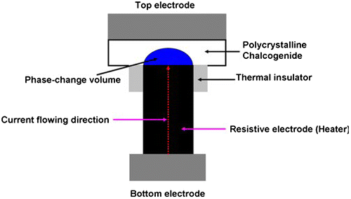
Figure 19. Various PRAM devices for threshold voltage scaling using: (a) additional electrode, reprinted with permission from [Citation154]; (b) phase-change nanowire, reprinted with permission from [Citation155]; (c) phase-change bridge, reprinted with permission from [Citation44]; and (d) carbon nanotube (CNT) electrode, reprinted with permission from [Citation160].
![Figure 19. Various PRAM devices for threshold voltage scaling using: (a) additional electrode, reprinted with permission from [Citation154]; (b) phase-change nanowire, reprinted with permission from [Citation155]; (c) phase-change bridge, reprinted with permission from [Citation44]; and (d) carbon nanotube (CNT) electrode, reprinted with permission from [Citation160].](/cms/asset/ff9bfb25-a12f-428e-9233-07fec3db4c1e/tsta_a_1332455_f0019_oc.gif)
Figure 20. Threshold field as a function of the length of the active phase-change region in a phase-change bridge memory for four different PCMs. Reprinted with permission from [Citation159]. ‘AIST’ refers to ‘Ag4In3Sb66Te27’.
![Figure 20. Threshold field as a function of the length of the active phase-change region in a phase-change bridge memory for four different PCMs. Reprinted with permission from [Citation159]. ‘AIST’ refers to ‘Ag4In3Sb66Te27’.](/cms/asset/f755c17c-539b-4463-b4df-ce81d635b443/tsta_a_1332455_f0020_oc.gif)
Figure 21. Various PRAM devices for ‘RESET’ current scaling using: (a) edge-contact type; (b) μTrench type; (c) ring-shaped type; (d) pillar type; (e) pore type; (f) cross-spacer type; and (g) dash type. Reprinted with permission from [Citation162].
![Figure 21. Various PRAM devices for ‘RESET’ current scaling using: (a) edge-contact type; (b) μTrench type; (c) ring-shaped type; (d) pillar type; (e) pore type; (f) cross-spacer type; and (g) dash type. Reprinted with permission from [Citation162].](/cms/asset/7e3e3ad3-6f14-403c-8b1a-0f08978ea8fe/tsta_a_1332455_f0021_oc.gif)
Figure 22. ‘RESET’ current as a function of equivalent contact diameter, showing a linear scaling trend with the effective contact area as the device feature size goes down. A constant ~40 MA/cm2 current density is required to program the PRAM cell. Reprinted with permission from [Citation14].
![Figure 22. ‘RESET’ current as a function of equivalent contact diameter, showing a linear scaling trend with the effective contact area as the device feature size goes down. A constant ~40 MA/cm2 current density is required to program the PRAM cell. Reprinted with permission from [Citation14].](/cms/asset/303995f1-7abe-4319-83d1-fb1df37fc0bf/tsta_a_1332455_f0022_oc.gif)
Figure 23. High-angle annular dark field (HAADF)-scanning transmission electron microscope (STEM) image of GeTe/Sb2Te3 superlatttice. Reprinted with permission from [Citation170].
![Figure 23. High-angle annular dark field (HAADF)-scanning transmission electron microscope (STEM) image of GeTe/Sb2Te3 superlatttice. Reprinted with permission from [Citation170].](/cms/asset/cb8ac507-1ef2-4696-ac23-7ef670f64845/tsta_a_1332455_f0023_oc.gif)
Figure 24. MLC for storing four logical states.
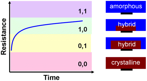
Figure 25. (a) Typical Rcell-Ipulse curve obtained by varying the current pulse amplitude for a mushroom phase-change memory cell. Reprinted with permission from [Citation174]. (b) Schematic illustrating the basic iterative programming concept using a sequence of adaptive write and verify steps. Reprinted with permission from [Citation179].
![Figure 25. (a) Typical Rcell-Ipulse curve obtained by varying the current pulse amplitude for a mushroom phase-change memory cell. Reprinted with permission from [Citation174]. (b) Schematic illustrating the basic iterative programming concept using a sequence of adaptive write and verify steps. Reprinted with permission from [Citation179].](/cms/asset/9bc744af-34f1-4fda-b1bb-7427372dabee/tsta_a_1332455_f0025_oc.gif)
Figure 26. Structure of the cross-point PRAM cell. Reprinted with permission from [Citation162].
![Figure 26. Structure of the cross-point PRAM cell. Reprinted with permission from [Citation162].](/cms/asset/5fc12d80-9392-4c26-88c0-770634a8434a/tsta_a_1332455_f0026_oc.gif)
Figure 27. Device structure and operation of VCCPCM. Reprinted with permission from [Citation190].
![Figure 27. Device structure and operation of VCCPCM. Reprinted with permission from [Citation190].](/cms/asset/5afd8320-b3ed-4ed3-805c-0c8a1c292295/tsta_a_1332455_f0027_oc.gif)
Figure 28. Schematics of the nanophotonic device using PCMs. Reprinted with permission from [Citation11].
![Figure 28. Schematics of the nanophotonic device using PCMs. Reprinted with permission from [Citation11].](/cms/asset/8965ea1f-64bd-4c4f-b54b-68d007a93bb9/tsta_a_1332455_f0028_oc.gif)
Figure 29. Eight clearly distinguishable levels are reached using this nanophotonic device by gradually changing the device transmission. Reprinted with permission from [Citation11].
![Figure 29. Eight clearly distinguishable levels are reached using this nanophotonic device by gradually changing the device transmission. Reprinted with permission from [Citation11].](/cms/asset/eab49213-6f76-4e1a-9b19-536f4222e0e2/tsta_a_1332455_f0029_oc.gif)