
Figures & data

Scheme 1. Schematic illustration of the structures and applications of HP-QDs composites discussed in this review. Produced with permission from [Citation69,Citation77]. © 2018 ACS Publications [Citation105,Citation117];. © 2017 Royal Society of Chemistry [Citation116,Citation121]; © 2017 ACS publications [Citation134]; © 2018 ScienceDirect [Citation122,Citation177]; © 2018 ScienceDirect.
![Scheme 1. Schematic illustration of the structures and applications of HP-QDs composites discussed in this review. Produced with permission from [Citation69,Citation77]. © 2018 ACS Publications [Citation105,Citation117];. © 2017 Royal Society of Chemistry [Citation116,Citation121]; © 2017 ACS publications [Citation134]; © 2018 ScienceDirect [Citation122,Citation177]; © 2018 ScienceDirect.](/cms/asset/0aadf15e-f984-4b32-b3aa-192ab8a6b1ec/tsta_a_1752115_sch0001_oc.jpg)
Scheme 2. An overview of the synthesis methods for various structures of HP-QDs based composites.
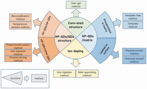
Figure 1. Schematic illustration of the synthesis strategies of (a) CsPbBr3 QD core/SiO2 shell structure. (b) CsPbBr3 QD core/TiO2 shell structure; transmission electron microscopy (TEM) images of (c) CsPbBr3 QDs (d) CsPbBr3 QD/TiO2 composites at single particle level. Produced with permission from [Citation69]. © 2018 ACS Publications, and [Citation70]. © 2018 Wiley.
![Figure 1. Schematic illustration of the synthesis strategies of (a) CsPbBr3 QD core/SiO2 shell structure. (b) CsPbBr3 QD core/TiO2 shell structure; transmission electron microscopy (TEM) images of (c) CsPbBr3 QDs (d) CsPbBr3 QD/TiO2 composites at single particle level. Produced with permission from [Citation69]. © 2018 ACS Publications, and [Citation70]. © 2018 Wiley.](/cms/asset/92767e62-7617-4621-b15f-669962f61790/tsta_a_1752115_f0001_oc.jpg)
Figure 2. (a) Schematic illustration of synthesis strategy of QD/silica composites. (b) The simplified synthesis of CsPbBr3/SiO2 composite; PL intensity of CsPbBr3/SiO2 composite under (c-d) heat, (e) 365 nm UV light (f) xenon lamp irradiation. Produced with permission from [Citation74]. © 2016 Wiley, and [Citation82]. © 2019 ScienceDirect.
![Figure 2. (a) Schematic illustration of synthesis strategy of QD/silica composites. (b) The simplified synthesis of CsPbBr3/SiO2 composite; PL intensity of CsPbBr3/SiO2 composite under (c-d) heat, (e) 365 nm UV light (f) xenon lamp irradiation. Produced with permission from [Citation74]. © 2016 Wiley, and [Citation82]. © 2019 ScienceDirect.](/cms/asset/03625760-23ab-4cb6-a54c-62c04438ba01/tsta_a_1752115_f0002_oc.jpg)
Figure 3. (a) Schematic illustration of MAPbBr3-QDs/PVDF synthesis via separate crystallization: Stage Ⅰ: mixture poured on the substrate; Stage II: evaporation of DMF; Stage III: removing the residual DMF. (b) Schematic illustration of the formation via Swelling-deswelling, and (c) via porous polymer template. Reproduced with permission from [Citation91,Citation92]. © 2016 Wiley, and [Citation105]. © 2017 Royal Society of Chemistry.
![Figure 3. (a) Schematic illustration of MAPbBr3-QDs/PVDF synthesis via separate crystallization: Stage Ⅰ: mixture poured on the substrate; Stage II: evaporation of DMF; Stage III: removing the residual DMF. (b) Schematic illustration of the formation via Swelling-deswelling, and (c) via porous polymer template. Reproduced with permission from [Citation91,Citation92]. © 2016 Wiley, and [Citation105]. © 2017 Royal Society of Chemistry.](/cms/asset/6bb7bb60-3c0a-4d3d-a7b4-8229cb53293b/tsta_a_1752115_f0003_oc.jpg)
Figure 4. (a) Schematic illustration of HP-QDs/MSP synthesis via physical stirring. (b-c) TEM images of HP-QDs/MSP obtained via capillary force. (d-e) TEM images of HP-QDs/MSP obtained via recrystallization. Reproduced with permission from [Citation101]. © 2016 Wiley, and [Citation102]. ©2016 ACS publication, and [Citation103]. © 2018 ACS publication.
![Figure 4. (a) Schematic illustration of HP-QDs/MSP synthesis via physical stirring. (b-c) TEM images of HP-QDs/MSP obtained via capillary force. (d-e) TEM images of HP-QDs/MSP obtained via recrystallization. Reproduced with permission from [Citation101]. © 2016 Wiley, and [Citation102]. ©2016 ACS publication, and [Citation103]. © 2018 ACS publication.](/cms/asset/b7f9005e-a0ad-40d7-99b8-ff7e67cda097/tsta_a_1752115_f0004_oc.jpg)
Figure 5. (a) Schematic illustration of the a-SiO2/HP-QDs synthesis. (b-d) TEM images of the a-SiO2/HP-QDs composite. (e) Size distribution of the loaded HP-QDs. Reproduced with permission from [Citation118]. © 2017 Wiley.
![Figure 5. (a) Schematic illustration of the a-SiO2/HP-QDs synthesis. (b-d) TEM images of the a-SiO2/HP-QDs composite. (e) Size distribution of the loaded HP-QDs. Reproduced with permission from [Citation118]. © 2017 Wiley.](/cms/asset/c7e2acd4-987f-4aa5-b928-416cf2fb08d7/tsta_a_1752115_f0005_oc.jpg)
Figure 6. Schematic illustrations of (a) the structures of crystal lattice of perovskite CsPbX3 before and after Mn2+doping; (b) the formation of CsPbBr3 and Eu3+:CsPbBr3 QDs via melt-quenching. (c-d) TEM images of Mn2+:CsPbX3 QDs prepared via HI. (e-f) TEM images of Eu3+:CsPbBr3 QDs prepared via melt-quenching. Reproduced with permission from [Citation121]. © 2017 ACS publications, and [Citation127]. © 2019 ScienceDirect.
![Figure 6. Schematic illustrations of (a) the structures of crystal lattice of perovskite CsPbX3 before and after Mn2+doping; (b) the formation of CsPbBr3 and Eu3+:CsPbBr3 QDs via melt-quenching. (c-d) TEM images of Mn2+:CsPbX3 QDs prepared via HI. (e-f) TEM images of Eu3+:CsPbBr3 QDs prepared via melt-quenching. Reproduced with permission from [Citation121]. © 2017 ACS publications, and [Citation127]. © 2019 ScienceDirect.](/cms/asset/dad8754e-2b8f-4d06-8490-2c38f82d44f5/tsta_a_1752115_f0006_oc.jpg)
Figure 7. Crystal structures of (a) CsPbBr3, (b) CsPb2Br5 and (c) dual-phase CsPbBr3/CsPb2Br5 composite. Reproduced with permission from [Citation134]. © 2018 ScienceDirect.
![Figure 7. Crystal structures of (a) CsPbBr3, (b) CsPb2Br5 and (c) dual-phase CsPbBr3/CsPb2Br5 composite. Reproduced with permission from [Citation134]. © 2018 ScienceDirect.](/cms/asset/641c02c5-8dbe-4197-918b-c91a229a2327/tsta_a_1752115_f0007_oc.jpg)
Figure 8. (a) PL spectra of CsPb(Br/I)3 QDs with varying Br/I ratio. (b) Picture of CsPb(Br/I)3 solution under UV light (top) and normal white light (bottom). (c) CIE color coordinates of CsPbBr3, CsPbBr1,2I1.8 and CsPbI3 separately. (d) Electroluminescence spectrum of CsPbBr3 QDs/SHFW composites, K2SiF6:Mn4+ and blue LED chip. (e) CIE color coordinate of CsPbBr3 QDs/SHFW/blue chip WLED. Reproduced with permission from [Citation83]. © 2018 ScienceDirect, and [Citation110]. © 2019 ACS Publications.
![Figure 8. (a) PL spectra of CsPb(Br/I)3 QDs with varying Br/I ratio. (b) Picture of CsPb(Br/I)3 solution under UV light (top) and normal white light (bottom). (c) CIE color coordinates of CsPbBr3, CsPbBr1,2I1.8 and CsPbI3 separately. (d) Electroluminescence spectrum of CsPbBr3 QDs/SHFW composites, K2SiF6:Mn4+ and blue LED chip. (e) CIE color coordinate of CsPbBr3 QDs/SHFW/blue chip WLED. Reproduced with permission from [Citation83]. © 2018 ScienceDirect, and [Citation110]. © 2019 ACS Publications.](/cms/asset/9da03d4f-df3b-49b2-8071-c18da9f3fe96/tsta_a_1752115_f0008_oc.jpg)
Figure 9. (a) Stability of PL quantum yield of CsPbBr3 QDs/SHFW in water. (b) Photos of CsPbBr3 QDs/SHFW in water after 3 months and 6 months under UV light (right) and normal white light (left). (c) Photos of CsPbBr3 QDs/SHFW in white light, UV light and under water drop. (d) PL spectra of CsPbBr3 QDs/SHFW composites. Reproduced with permission from [Citation110]. © 2019 ACS Publications.
![Figure 9. (a) Stability of PL quantum yield of CsPbBr3 QDs/SHFW in water. (b) Photos of CsPbBr3 QDs/SHFW in water after 3 months and 6 months under UV light (right) and normal white light (left). (c) Photos of CsPbBr3 QDs/SHFW in white light, UV light and under water drop. (d) PL spectra of CsPbBr3 QDs/SHFW composites. Reproduced with permission from [Citation110]. © 2019 ACS Publications.](/cms/asset/ba4214f4-5149-437a-a24a-b17a97773dac/tsta_a_1752115_f0009_oc.jpg)
Figure 10. Energy level diagram of (a) MAPbI3/TiO2, (b) CsPbBr3/TiO2 and CsPbBr3/ZrO2. (c) Schematic illustration of MAPbI3/TiO2 NTs composites. (d) I–V curves and (e) I-t curves of pure TiO2 NTs, MAPbI3/TiO2 NTs and MAPbI3/TiO2 NWs under darkness, 350 nm light, 700 nm light. Reproduced with permission from [Citation113]. © 2017 Wiley, and [Citation157]. © 2018 ACS Publications.
![Figure 10. Energy level diagram of (a) MAPbI3/TiO2, (b) CsPbBr3/TiO2 and CsPbBr3/ZrO2. (c) Schematic illustration of MAPbI3/TiO2 NTs composites. (d) I–V curves and (e) I-t curves of pure TiO2 NTs, MAPbI3/TiO2 NTs and MAPbI3/TiO2 NWs under darkness, 350 nm light, 700 nm light. Reproduced with permission from [Citation113]. © 2017 Wiley, and [Citation157]. © 2018 ACS Publications.](/cms/asset/dc876ed1-49ec-4b1a-94e6-18aaa61721c9/tsta_a_1752115_f0010_oc.jpg)
Figure 11. (a) Yield of product from CO2 reduction and (b) quantum efficiency using CsPbBr3 QD and CsPbBr3 QD/GO composite as the photocatalyst, respectively. (c) I-t curves under −0.4 V and electrochemical impedance Nyquist plots under 150 mW/cm2 and −0.4 V. Reproduced with permission from [Citation116]. © 2017 ACS Publications.
![Figure 11. (a) Yield of product from CO2 reduction and (b) quantum efficiency using CsPbBr3 QD and CsPbBr3 QD/GO composite as the photocatalyst, respectively. (c) I-t curves under −0.4 V and electrochemical impedance Nyquist plots under 150 mW/cm2 and −0.4 V. Reproduced with permission from [Citation116]. © 2017 ACS Publications.](/cms/asset/4d2401ed-5e82-4b18-84ce-2bac72382a54/tsta_a_1752115_f0011_oc.jpg)
Figure 12. (a) Schematic illustration and (b) EQE of traditional silicon solar cell. (c) Energy level diagram of Mn2+:CsPbCl3. (d) Working lifetime of pure Mn2+, CsPbCl3 QDs and Mn2+:CsPbCl3 QDs. (e) Schematic illustration and (f) Surface reflectance spectra of silicon solar cell with Mn2+:CsPbCl3 layer. Influence of Mn2+:CsPbCl3 QDs layer on second-reflection with different concentration. (g) 3 mg/mL and (h) 18 mg/mL. Reproduced with permission from [Citation122]. © 2018 ScienceDirect.
![Figure 12. (a) Schematic illustration and (b) EQE of traditional silicon solar cell. (c) Energy level diagram of Mn2+:CsPbCl3. (d) Working lifetime of pure Mn2+, CsPbCl3 QDs and Mn2+:CsPbCl3 QDs. (e) Schematic illustration and (f) Surface reflectance spectra of silicon solar cell with Mn2+:CsPbCl3 layer. Influence of Mn2+:CsPbCl3 QDs layer on second-reflection with different concentration. (g) 3 mg/mL and (h) 18 mg/mL. Reproduced with permission from [Citation122]. © 2018 ScienceDirect.](/cms/asset/35ea5b56-6267-4fbe-bfd5-3643c42d8298/tsta_a_1752115_f0012_oc.jpg)
Figure 13. (a) TEM image and (b) XRD pattern of pure CsPbBr3 QDs. (c) Schematic illustration of the device structure. (d) Optical absorption and (e) PL spectrum of pure CsPbBr3 QDs, PQT-12 and CsPbBr3 QDs/PQT-12 composites. Optical response of CsPbBr3 QDs/PQT-12 composites. Reproduced with permission from [Citation178]. © 2019 Wiley.
![Figure 13. (a) TEM image and (b) XRD pattern of pure CsPbBr3 QDs. (c) Schematic illustration of the device structure. (d) Optical absorption and (e) PL spectrum of pure CsPbBr3 QDs, PQT-12 and CsPbBr3 QDs/PQT-12 composites. Optical response of CsPbBr3 QDs/PQT-12 composites. Reproduced with permission from [Citation178]. © 2019 Wiley.](/cms/asset/af649b98-45ca-4a5e-969c-1ecf7c192154/tsta_a_1752115_f0013_oc.jpg)