
Figures & data
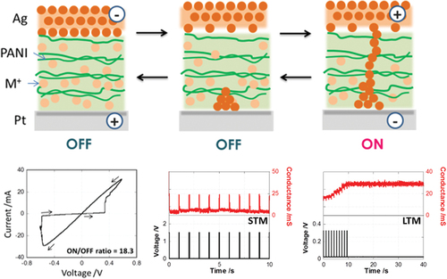
Figure 1. Chemical structure of polyaniline.
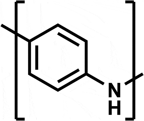
Figure 2. (a) Device architecture for Type I: Cu2+- doped devices; (b) I-V response to ± 0.6 V input at 1 hz sweep rate; (c, d) Conductance response of pulsed inputs of width (W) = 0.05 s at intervals (T) = 1 s for voltage amplitudes (V) = 1.5 V (c, STM) or 0.3 V (d, LTM).
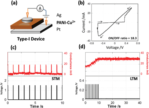
Figure 3. (a) Device architecture for Type II: Ag+- doped devices; (b) I-V response to ± 0.6 V input at 1 hz sweep rate.; (c – f) conductance response pulsed input. (c) input voltage (V) = 0.4 V, pulse width (W) = 0.5 s, interval (T) = 0.5 s; (d) V = 0.6 V, W = 0.5 s, T = 0.5 s; (e) V = 2.9 V, W = 0.1 s, T = 2 s; (f) V = 2.9 V, W = 0.1 s, T = 0.2 s.
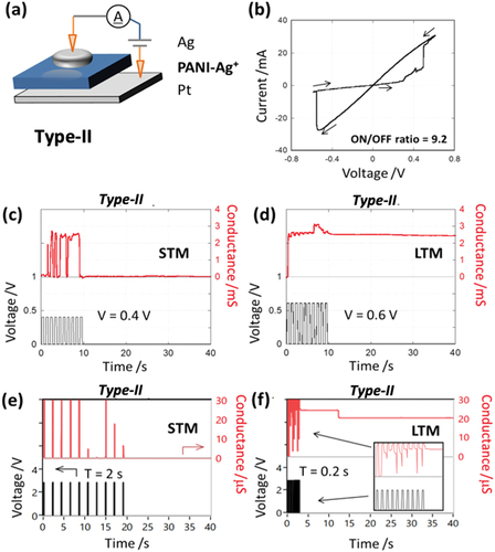
Figure 4. (a) Magnified region of the pulse response for Type-II devices (Figure 1d). (b) Histogram of G0 fitted by Gaussian curve (blue line). The number corresponds to each step observed in the change of conductance.
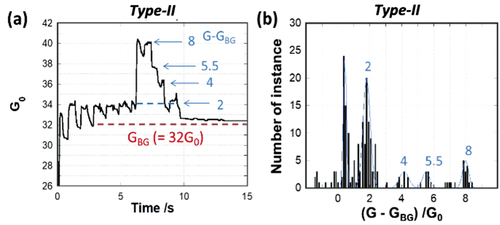
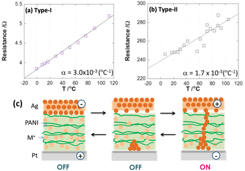
Figure 5. (a-b) Temperature dependence of resistance the on states. (c) Proposed mechanism of resistive switching for metal ion-doped device.