
Figures & data
Figure 1. Cross-sectional structure of (a) the fabricated In-Ga-Zn oxide (IGZO) thin-film transistor (TFT) with a temperature sensor on it and (b) a sample for evaluating the sensor with a heating element.
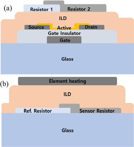
Figure 2. Optical microscopic images: (a) temperature sensor under IGZO TFT, (b) temperature sensor on IGZO TFT.
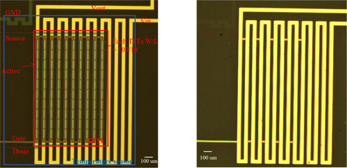
Figure 3. Output voltages and linear fit curve of the proposed temperature sensor.
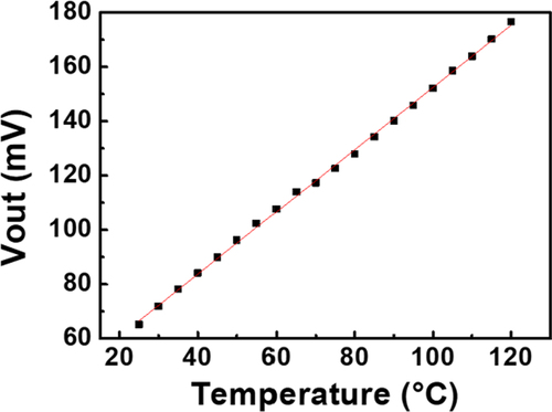
Figure 4. Hysteresis of the proposed temperature sensor.
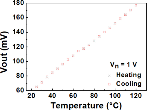
Figure 5. Repeatability of the proposed temperature sensor.
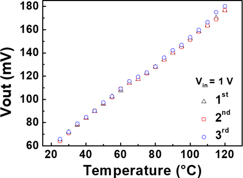
Table 1. Characteristics of the thin-film temperature sensor.
Figure 6. Electrical characteristics of the amorphous IGZO (a-IGZO) TFTs with a thin-film temperature sensor on it. (a) Transfer characteristics and (b) output characteristics.
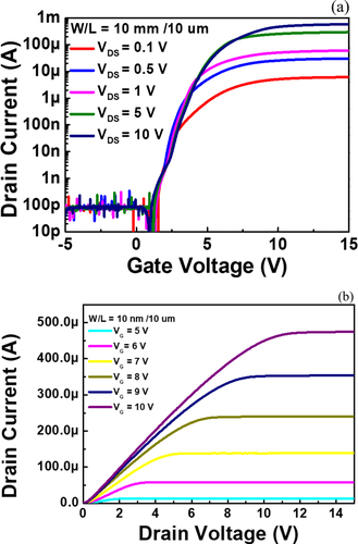
Figure 7. Positive-bias illumination stress of the a-IGZO TFTs. (a) Drain current of the a-IGZO TFT without the light-shielding (LS) layer and (b) drain current of the a-IGZO TFT with the LS layer.
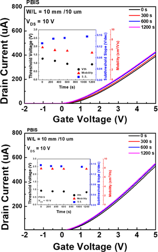
Figure 8. (a) Optical microscopic image of the TFT with an embedded temperature sensor, forward-looking infrared (FLIR) images at (b) VDS = 5 V, (c) 13 V, (d) 15 V, (e) 18 V (e), and (f) 20 V.
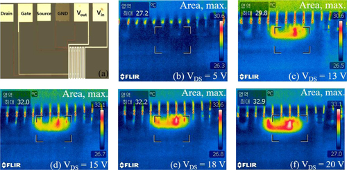
Figure 9. Measured output voltages of the temperature sensor and FLIR temperature according to the IGZO TFT currents.
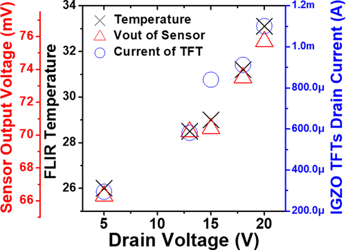
Table 2. Temperature sensor embedded TFT.