Figures & data
Figure 1. (a) Schematic diagram of the bilayer IGZO/GZO top-gate TFT structure and the Ga:Zn ALD subcycle ratios for the growth of the GZO layers used in the S1–S3 devices, (b) Transfer curves, and (c) electrical parameters of the S1-S3 TFTs (average values extracted from 10 evaluated devices for each condition). (d) Time evolution of Vth under PBTS (temperature = 60°C, bias = 2 MV cm−1 for 1 h) and NBIS (warm white light = 1000 lux, bias = −2 MV cm−1 for 1 h) for the S1–S3 devices.
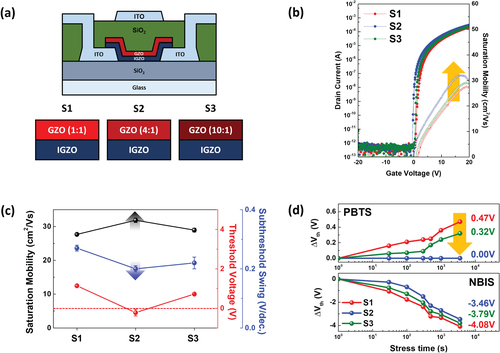
Table 1. Electrical parameters were obtained from the transfer curves of the PEALD IGZO/GZO TFTs (average values (± standard deviation) extracted from 10 devices for each condition).
Figure 2. The chemical, optical, and physical properties of the PEALD GZO thin films (G1–G3): (a) XPS spectra of O 1 s; (b) optical band gap; (c) crystallinity; and (d) root mean square (RMS) roughness.
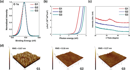
Table 2. Elemental compositions (Ga, Zn, and O were analyzed before surface etching) and carbon impurities (C was analyzed after surface etching) of PEALD GZO films obtained by XPS analyses with respect to Ga: Zn subcycle ratios.
Figure 3. (a) PL spectra of the GZO thin films (G1–G3) and (b) magnified portion (photon energy from 1.5 to 1.85 eV). (c) Schematic illustrating the deexcitation of electrons between subgap defect states.
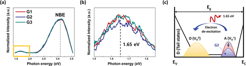
Figure 4. Schematic band diagram of bilayer IGZO/GZO TFTs (S1-S3) with different GZO compositions. The Ga: Zn ALD subcycle ratios of the GZO films are (a) 1:1, (b) 4:1, and (c) 10:1.
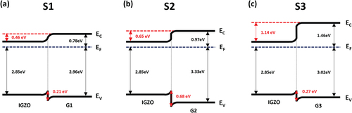
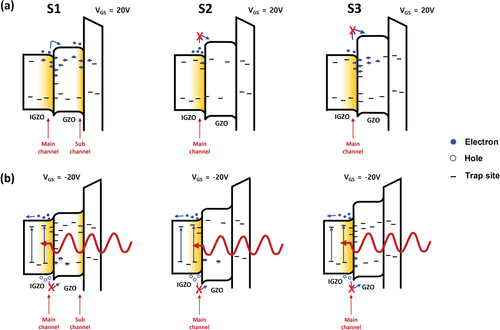
Figure 5. Degradation mechanism of IGZO/GZO TFTs (S1-S3) under (a) PBTS (60°C, 2 MV cm−1) and (b) NBIS (1000 lux, −2 MV cm−1).