Figures & data
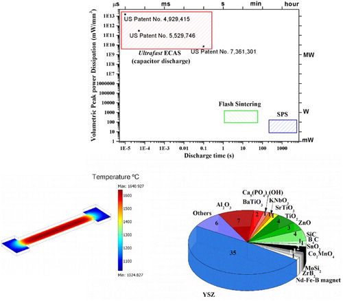
Figure 1. Some snapshots taken from initial work linked to FS. (a) Patent front page of ‘electrical glower light’ dated 1897 taken from original document GB189719424. The lamp described in this document employed a magnesia glower (7 mm length, hollow cylinder outer diameter 1.4 mm and inner diameter 0.4 mm). The glower was first heated using a flame, when it reached a sufficient temperature an AC power source was switched on (0.23 A, 118 V) and the 27 W lamp emitted an intensity of 26 cd (candles). (b) Snapshot of document published in 1908 on electroluminescence of selected oxides [Citation8]. In this work, when the material could not be prepared by melting is was produced by sintering pastes. (c) Drawing showing an experimental setup for FS (see top heading) developed by Hill et al. [Citation9] in 1952. A ceramic lining allowed electrical insulation between the punches and the die, thus allowing current to entirely flow across the powder.
![Figure 1. Some snapshots taken from initial work linked to FS. (a) Patent front page of ‘electrical glower light’ dated 1897 taken from original document GB189719424. The lamp described in this document employed a magnesia glower (7 mm length, hollow cylinder outer diameter 1.4 mm and inner diameter 0.4 mm). The glower was first heated using a flame, when it reached a sufficient temperature an AC power source was switched on (0.23 A, 118 V) and the 27 W lamp emitted an intensity of 26 cd (candles). (b) Snapshot of document published in 1908 on electroluminescence of selected oxides [Citation8]. In this work, when the material could not be prepared by melting is was produced by sintering pastes. (c) Drawing showing an experimental setup for FS (see top heading) developed by Hill et al. [Citation9] in 1952. A ceramic lining allowed electrical insulation between the punches and the die, thus allowing current to entirely flow across the powder.](/cms/asset/db156435-7025-4780-8aac-72a880cf2b3c/yaac_a_1251051_f0001_c.jpg)
Figure 2. Volumetric peak power dissipation vs. electrical discharge time for different sintering ECAS techniques. The referred operating conditions are taken from typical processing parameters reported in the literature. The peak power density for Ultrafast ECAS was calculated by assuming a sample volume of 63–625 mm3 (current density of 100–1500 A mm−2 and voltages of 3 V–30 kV). The peak power densities in FS are derived from Raj et al. [Citation12], even higher peak dissipation can be reached during switching from voltage to current control mode. The discharge time does not account for incubation time. The peak power densities in SPS have been calculated assuming a power of 1–10 kW for a graphite moulding having diameter of 20 mm.
![Figure 2. Volumetric peak power dissipation vs. electrical discharge time for different sintering ECAS techniques. The referred operating conditions are taken from typical processing parameters reported in the literature. The peak power density for Ultrafast ECAS was calculated by assuming a sample volume of 63–625 mm3 (current density of 100–1500 A mm−2 and voltages of 3 V–30 kV). The peak power densities in FS are derived from Raj et al. [Citation12], even higher peak dissipation can be reached during switching from voltage to current control mode. The discharge time does not account for incubation time. The peak power densities in SPS have been calculated assuming a power of 1–10 kW for a graphite moulding having diameter of 20 mm.](/cms/asset/457dc04f-85cb-45ff-aa8a-f3c3023b9cda/yaac_a_1251051_f0002_c.jpg)
Figure 3. The temperature-dependence of conductivity of typical metallic, semiconductor (narrow and wide band gap) and ionic conductor, W (Tm = 3380°C) [Citation21], Cu (Tm = 1084°C) [Citation22], B4.3C (Tm* = 2447°C) [Citation23], SiC (Tm* = 2730°C, 3.1 eV) [Citation24], YSZ (Tm ≈ 2700°C) [Citation25], BaTiO3 (Tm = 1618°C, 1.55 eV) [Citation26], Al2O3 (Tm = 2050°C) [Citation27]. Colour coded: metals (grey), semiconductors (green), oxygen ion conductors (blue) and insulating oxides (red). * The material might decompose before melting.
![Figure 3. The temperature-dependence of conductivity of typical metallic, semiconductor (narrow and wide band gap) and ionic conductor, W (Tm = 3380°C) [Citation21], Cu (Tm = 1084°C) [Citation22], B4.3C (Tm* = 2447°C) [Citation23], SiC (Tm* = 2730°C, 3.1 eV) [Citation24], YSZ (Tm ≈ 2700°C) [Citation25], BaTiO3 (Tm = 1618°C, 1.55 eV) [Citation26], Al2O3 (Tm = 2050°C) [Citation27]. Colour coded: metals (grey), semiconductors (green), oxygen ion conductors (blue) and insulating oxides (red). * The material might decompose before melting.](/cms/asset/55c24605-6e08-4d9b-ad28-e5af1a41b1d3/yaac_a_1251051_f0003_c.jpg)
Figure 4. Schematic representation of different FS experimental setups: (a) sample is suspended in a furnace using two Pt wire electrodes (adapted from Cologna et al. [Citation33]); (b) sample is pressed between two electrodes (adapted from Caliman et al. [Citation34]); (c) a commercially available SPS machine is used (adapted from Grasso et al. [Citation35]); (d) contactless mode where a plasma is used to carry current across the sample (adapted from Saunders et al. [Citation36]); and (e) setup developed at Rutgers University (RU Tech ID#: 2014-056).
![Figure 4. Schematic representation of different FS experimental setups: (a) sample is suspended in a furnace using two Pt wire electrodes (adapted from Cologna et al. [Citation33]); (b) sample is pressed between two electrodes (adapted from Caliman et al. [Citation34]); (c) a commercially available SPS machine is used (adapted from Grasso et al. [Citation35]); (d) contactless mode where a plasma is used to carry current across the sample (adapted from Saunders et al. [Citation36]); and (e) setup developed at Rutgers University (RU Tech ID#: 2014-056).](/cms/asset/f50d720f-e17a-4895-91bf-0d3a4775ba1c/yaac_a_1251051_f0004_c.jpg)
Figure 5. (a) Power density and shrinkage relationship in 3YSZ under a field of 100 V cm−1 (DC). (b) Powder density and specimen temperature measured by lattice thermal expansion in situ by synchrotron during FS of 3YSZ under a field of 170 V cm−1 (DC). Adapted from Raj [Citation19] and Lebrun et al. [Citation62].
![Figure 5. (a) Power density and shrinkage relationship in 3YSZ under a field of 100 V cm−1 (DC). (b) Powder density and specimen temperature measured by lattice thermal expansion in situ by synchrotron during FS of 3YSZ under a field of 170 V cm−1 (DC). Adapted from Raj [Citation19] and Lebrun et al. [Citation62].](/cms/asset/e53af13e-ed0b-4533-8cd8-b60e4ce46001/yaac_a_1251051_f0005_c.jpg)
Table 1. Sets of real-time input and output parameters that can be adjusted and recorded during FS.
Figure 6. (a) FS setup and dimensions of DBS green sample (adapted from Naik et al. [Citation63]). (b) Sketch of the experimental setup for dilatometric measurements which can be coupled with impedance spectroscopy during the FS event. LVDT and Pt–Pt 10%Rh thermocouple are used to measure the linear shrinkage. Adapted from Francis et al. [Citation49].
![Figure 6. (a) FS setup and dimensions of DBS green sample (adapted from Naik et al. [Citation63]). (b) Sketch of the experimental setup for dilatometric measurements which can be coupled with impedance spectroscopy during the FS event. LVDT and Pt–Pt 10%Rh thermocouple are used to measure the linear shrinkage. Adapted from Francis et al. [Citation49].](/cms/asset/417a2950-c701-4cf6-897b-2948744537d4/yaac_a_1251051_f0006_c.jpg)
Table 2. Physical principle and probing position for the different temperature measurement methods used in the literature.
Figure 7. Emission spectra collected in situ for W powder matching black body radiation and temperatures (obtained from black body radiation fitting) at different time intervals [Citation68].
![Figure 7. Emission spectra collected in situ for W powder matching black body radiation and temperatures (obtained from black body radiation fitting) at different time intervals [Citation68].](/cms/asset/722eeeee-169a-463c-88d9-3363535e0e5f/yaac_a_1251051_f0007_c.jpg)
Figure 8. The arrangement for in situ XRD experiments at the Pohang Light Source II. Adapted from Terauds et al. [Citation71].
![Figure 8. The arrangement for in situ XRD experiments at the Pohang Light Source II. Adapted from Terauds et al. [Citation71].](/cms/asset/12190c96-1f7d-4fc1-beb8-eed91503b7e0/yaac_a_1251051_f0008_c.jpg)
Figure 9. Pie chart showing the number of papers published on FS, grouped by material type. The conductivity mechanism (at TOnset) is colour coded: oxygen ion conductors (blue), insulating oxides (red), semiconductors (green), metals (grey). Some materials might show a mixed conductivity mode depending on the temperature. Some of the materials have been consolidated as composites.
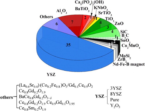
Figure 10. (a) Research papers published starting from July 2010 till the May 2016. (b) Pie chart showing the nationality of first author’s institution.
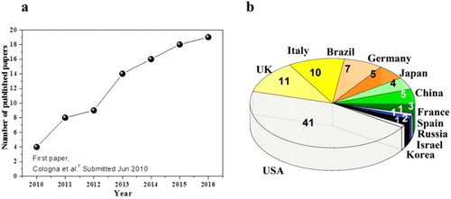
Figure 11. (a) Arrhenius plot of volumetric power dissipation for several different ceramics sintered by FS using DC fields. The furnace heating rate was 10°C min−1 and the currents were limited to 80 mA mm−2. The dark grey region with a power dissipation ranging from 7 to 40 mW mm−3 highlights the ‘abrupt’ increase in electrical conductivity of the sample. The sample is DBS with gauge length 20 mm and cross-section 3 × 1.6 mm2. (b) Linear shrinkage measured during FS of 3YSZ under various DC electric fields. (c) Multi-layered NiO–ZrO2 anode to 8YSZ electrolyte with and without the applied field (DC) heated at a rate of 10°C min−1. Adapted from Lebrun et al. [Citation62], Cologna et al. [Citation5], and Francis et al. [Citation49], respectively.
![Figure 11. (a) Arrhenius plot of volumetric power dissipation for several different ceramics sintered by FS using DC fields. The furnace heating rate was 10°C min−1 and the currents were limited to 80 mA mm−2. The dark grey region with a power dissipation ranging from 7 to 40 mW mm−3 highlights the ‘abrupt’ increase in electrical conductivity of the sample. The sample is DBS with gauge length 20 mm and cross-section 3 × 1.6 mm2. (b) Linear shrinkage measured during FS of 3YSZ under various DC electric fields. (c) Multi-layered NiO–ZrO2 anode to 8YSZ electrolyte with and without the applied field (DC) heated at a rate of 10°C min−1. Adapted from Lebrun et al. [Citation62], Cologna et al. [Citation5], and Francis et al. [Citation49], respectively.](/cms/asset/9881e44c-2417-4cc8-adcb-7681fda14564/yaac_a_1251051_f0011_c.jpg)
Table 3. Experimental procedures for FS, including materials, conductivity mode, crystallite size of starting powder, sample size, FS condition current, voltages, relative density and grain size of the produced materials.
Figure 12. SEM micrographs of (a) 3YSZ, (b) 8YSZ and (c) Y2O3 FSed as described in the text above using DC fields. Adapted from Baraki et al. [Citation86], M'Peko et al. [Citation70], and Yoshida et al. [Citation47], respectively.
![Figure 12. SEM micrographs of (a) 3YSZ, (b) 8YSZ and (c) Y2O3 FSed as described in the text above using DC fields. Adapted from Baraki et al. [Citation86], M'Peko et al. [Citation70], and Yoshida et al. [Citation47], respectively.](/cms/asset/1e31d3d9-2595-46f7-8fb6-3478edf23d62/yaac_a_1251051_f0012_b.gif)
Figure 13. Effect of applied electric field (0–1000 V cm−1) on the shrinkage for (a) pure Al2O3 and (b) MgO (0.25 wt-% MgO) doped Al2O3. The resulting SEM micrographs for MgO-doped Al2O3 obtained using (c) FS (1000 V cm−1, DC) TF = 1260°C) and (d) conventional sintering (1550°C for 1 h), the resulting grain sizes were 0.8 and 1.5 µm. In both cases the furnace heating rate was 10°C min−1. Adapted from Cologna et al. [Citation33].
![Figure 13. Effect of applied electric field (0–1000 V cm−1) on the shrinkage for (a) pure Al2O3 and (b) MgO (0.25 wt-% MgO) doped Al2O3. The resulting SEM micrographs for MgO-doped Al2O3 obtained using (c) FS (1000 V cm−1, DC) TF = 1260°C) and (d) conventional sintering (1550°C for 1 h), the resulting grain sizes were 0.8 and 1.5 µm. In both cases the furnace heating rate was 10°C min−1. Adapted from Cologna et al. [Citation33].](/cms/asset/e2cbcf22-5c19-426f-9cb9-e55586d364a1/yaac_a_1251051_f0013_b.gif)
Figure 14. SEM micrographs of SrTiO3 obtained using (a) FS (150 V cm−1 DC), TF = 1200°C) and (b) conventional sintering (1400°C for 1 h). Adapted from Yoshida et al. [Citation47].
![Figure 14. SEM micrographs of SrTiO3 obtained using (a) FS (150 V cm−1 DC), TF = 1200°C) and (b) conventional sintering (1400°C for 1 h). Adapted from Yoshida et al. [Citation47].](/cms/asset/b2e93191-df16-41fc-97d4-360f044c8466/yaac_a_1251051_f0014_b.gif)
Figure 15. (a) Microstructure of FSed BaTiO3 at an applied voltage (DC) of 250 V cm−1 and current limit of 9.3 mA mm−2, TF = 822°C. (b) TEM bright field image and the electron diffraction pattern of a secondary phase in flash-sintered BaTiO3 at an applied voltage of 100 V cm−1 (DC), TF = 1020°C for 60 s. (c) Microstructure of flash-sintered KNbO3 with applied electric field of 600 V cm−1 (DC), TF = 750°C. Adapted from M'Peko et al. [Citation94], Uehashi et al. [Citation77], and Shomrat et al. [Citation78], respectively.
![Figure 15. (a) Microstructure of FSed BaTiO3 at an applied voltage (DC) of 250 V cm−1 and current limit of 9.3 mA mm−2, TF = 822°C. (b) TEM bright field image and the electron diffraction pattern of a secondary phase in flash-sintered BaTiO3 at an applied voltage of 100 V cm−1 (DC), TF = 1020°C for 60 s. (c) Microstructure of flash-sintered KNbO3 with applied electric field of 600 V cm−1 (DC), TF = 750°C. Adapted from M'Peko et al. [Citation94], Uehashi et al. [Citation77], and Shomrat et al. [Citation78], respectively.](/cms/asset/9fb12181-7e55-4e90-a6b0-009e4be2c3a7/yaac_a_1251051_f0015_b.gif)
Figure 16. Microstructures of ZnO obtained using at 80 V cm−1 (AC) stopped (a) before and (b) after FS as well as fully sintered specimens at (c) 0 V cm−1 for 2 h, (d) 40 V cm−1 for 1 h, (e) 80 V cm−1 for 2 h and (f) 160 V cm−1 1 h, with TF = 700°C. Current densities were between 54 and 151 mA mm−2. Adapted from Schmerbauch et al. [Citation41].
![Figure 16. Microstructures of ZnO obtained using at 80 V cm−1 (AC) stopped (a) before and (b) after FS as well as fully sintered specimens at (c) 0 V cm−1 for 2 h, (d) 40 V cm−1 for 1 h, (e) 80 V cm−1 for 2 h and (f) 160 V cm−1 1 h, with TF = 700°C. Current densities were between 54 and 151 mA mm−2. Adapted from Schmerbauch et al. [Citation41].](/cms/asset/8b2256ca-9415-40ea-abf9-733b416d3968/yaac_a_1251051_f0016_b.gif)
Figure 17. (a) SEM micrograph of FSed Co2MnO4 (DC). (Adapted from Prette et al. [Citation37]). (b) The relative density and grain size vs. discharge time for FSPSed (pulsed DC) ZrB2 sample and (c) SEM microstructure of ZrB2 after 35 s discharge. (Adapted from Grasso et al. [Citation35] (d) SEM micrograph of Nd–Fe–B type permanent magnetic material with aligned nanocrystalline platelike grains. Adapted from Castle et al. [Citation98]).
![Figure 17. (a) SEM micrograph of FSed Co2MnO4 (DC). (Adapted from Prette et al. [Citation37]). (b) The relative density and grain size vs. discharge time for FSPSed (pulsed DC) ZrB2 sample and (c) SEM microstructure of ZrB2 after 35 s discharge. (Adapted from Grasso et al. [Citation35] (d) SEM micrograph of Nd–Fe–B type permanent magnetic material with aligned nanocrystalline platelike grains. Adapted from Castle et al. [Citation98]).](/cms/asset/cbeed7b7-d49b-4c48-99df-75ca5da1aa11/yaac_a_1251051_f0017_c.jpg)
Figure 18. (a) Temperature of 8YSZ samples (0.6–0.9 mm thick) under constant voltage (8–8.5 V (DC)) as function of time (no current limit). Inset: decrease in resistance (AC real component) divided by its room temperature reference value. (b) Empirical relationship between DC electric field and incubation time for FS of 3YSZ at different isotherms TF (1000, 1200, 1275 and 1300°C). Adapted from Park and Chen [Citation69] and Naik [Citation106], respectively.
![Figure 18. (a) Temperature of 8YSZ samples (0.6–0.9 mm thick) under constant voltage (8–8.5 V (DC)) as function of time (no current limit). Inset: decrease in resistance (AC real component) divided by its room temperature reference value. (b) Empirical relationship between DC electric field and incubation time for FS of 3YSZ at different isotherms TF (1000, 1200, 1275 and 1300°C). Adapted from Park and Chen [Citation69] and Naik [Citation106], respectively.](/cms/asset/6ec2a60d-45a6-4535-aae4-9b312abdcb23/yaac_a_1251051_f0018_c.jpg)
Figure 19. (a) Effect of particle size on the FS behaviour of 3YSZ, the shrinkage is plotted against furnace temperature with and without field (100 V cm−1 (DC)) (Adapted from Francis et al. [Citation82]). (b) Difference in conductivity for polycrystalline and single crystal 8YSZ and (c) the resulting power absorption of dense specimens while heating in flash mode. The figures were kindly provided by Professor Jian Luo from University of California, San Diego Jian Luo PDP. 2016. Private communication.
![Figure 19. (a) Effect of particle size on the FS behaviour of 3YSZ, the shrinkage is plotted against furnace temperature with and without field (100 V cm−1 (DC)) (Adapted from Francis et al. [Citation82]). (b) Difference in conductivity for polycrystalline and single crystal 8YSZ and (c) the resulting power absorption of dense specimens while heating in flash mode. The figures were kindly provided by Professor Jian Luo from University of California, San Diego Jian Luo PDP. 2016. Private communication.](/cms/asset/0c8f0018-a681-4ef7-88a6-5d9d314ef33b/yaac_a_1251051_f0019_c.jpg)
Figure 20. Shrinkage strain of 3YSZ samples under different uniaxial pressures using the setup shown in (b) in a 100 V cm−1 applied field. Adapted from Francis [Citation54].
![Figure 20. Shrinkage strain of 3YSZ samples under different uniaxial pressures using the setup shown in Figure 4(b) in a 100 V cm−1 applied field. Adapted from Francis [Citation54].](/cms/asset/19301d31-9e82-4514-81d0-e2fd2f66ef28/yaac_a_1251051_f0020_c.jpg)
Figure 21. (a) Measured electric power dissipation plotted against furnace temperature and (b) measured conductivity as function of the reciprocal of the estimated TS for FS ZnO using four different atmospheres (in a 300 V cm−1 DC electric field). Adapted from Zhang and Luo [Citation96].
![Figure 21. (a) Measured electric power dissipation plotted against furnace temperature and (b) measured conductivity as function of the reciprocal of the estimated TS for FS ZnO using four different atmospheres (in a 300 V cm−1 DC electric field). Adapted from Zhang and Luo [Citation96].](/cms/asset/13272943-e73a-4fb1-a0aa-1cd6c012bff1/yaac_a_1251051_f0021_c.jpg)
Figure 22. FS attempts in β-Al2O3 with different electrode materials and atmospheres during isothermal at 550°C under an applied AC field of 100 V cm−1 (AC). FS occurred when Ag electrodes were used instead of Pt. Adapted from Caliman et al. [Citation34].
![Figure 22. FS attempts in β-Al2O3 with different electrode materials and atmospheres during isothermal at 550°C under an applied AC field of 100 V cm−1 (AC). FS occurred when Ag electrodes were used instead of Pt. Adapted from Caliman et al. [Citation34].](/cms/asset/39ab547f-671d-4200-ba53-60f0e6b74e78/yaac_a_1251051_f0022_c.jpg)
Table 4. Bulk effects occurring within the material as result of DC bias applied across sample during FS.
Figure 23. (a) The relationship between AC conductivity measured at room temperature plotted against the amount of oxygen deficiency of 3YSZ. Adapted from Sano et al. [Citation113]. The sample was reduced in controlled conditions using electrochemical reduction. (b) Electrical conductivity (real component) for 12YSZ measured using IS for low and high sub-stoichiometric (ZrO2−X) samples. Adapted from Levy et al. [Citation114].
![Figure 23. (a) The relationship between AC conductivity measured at room temperature plotted against the amount of oxygen deficiency of 3YSZ. Adapted from Sano et al. [Citation113]. The sample was reduced in controlled conditions using electrochemical reduction. (b) Electrical conductivity (real component) for 12YSZ measured using IS for low and high sub-stoichiometric (ZrO2−X) samples. Adapted from Levy et al. [Citation114].](/cms/asset/5d87b42f-bbf7-4ff2-9041-f90a1758db7f/yaac_a_1251051_f0023_b.gif)
Figure 24. SEM micrograph of fracture in 8YSZ along a cross-section parallel to the electric field (50 mA mm−2, (DC) electric-loading time: 1440 min at TF of 1250°C, thickness: 1.5 mm). Adapted from Kim et al. [Citation116].
![Figure 24. SEM micrograph of fracture in 8YSZ along a cross-section parallel to the electric field (50 mA mm−2, (DC) electric-loading time: 1440 min at TF of 1250°C, thickness: 1.5 mm). Adapted from Kim et al. [Citation116].](/cms/asset/301ce1e4-b02e-4020-8810-62b93790704d/yaac_a_1251051_f0024_c.jpg)
Figure 25. SEM micrographs of the fractured surfaces of FSed ZnO (300 V cm−1, DC): (a) near the anode; and (b) cathode, respectively. (Adapted from Zhang et al. [Citation56]). A schematic of the Peltier effect occurring during FS for an n-type semiconductor was added by us.
![Figure 25. SEM micrographs of the fractured surfaces of FSed ZnO (300 V cm−1, DC): (a) near the anode; and (b) cathode, respectively. (Adapted from Zhang et al. [Citation56]). A schematic of the Peltier effect occurring during FS for an n-type semiconductor was added by us.](/cms/asset/6b6e0029-f94d-4d04-9dd8-499a0adce99d/yaac_a_1251051_f0025_c.jpg)
Figure 26. Images of 5L5NS during 150 V cm−1 (DC) when the furnace temperature was (a) T < TOnset and (b) TOnset < T < TSoft of EFIS. The anode and cathode are at the top and the bottom, respectively. (c) Photoemission spectra at the 200 V cm−1 test condition ranging from 350 to 900 nm for NS and 2L8NS. Note: Intensity of 2L8NS was offset by an arbitrary amount for comparison. (Adapted from McLaren et al. [Citation123]). (d) Emission spectra of Na and Li oxidation (added by us).
![Figure 26. Images of 5L5NS during 150 V cm−1 (DC) when the furnace temperature was (a) T < TOnset and (b) TOnset < T < TSoft of EFIS. The anode and cathode are at the top and the bottom, respectively. (c) Photoemission spectra at the 200 V cm−1 test condition ranging from 350 to 900 nm for NS and 2L8NS. Note: Intensity of 2L8NS was offset by an arbitrary amount for comparison. (Adapted from McLaren et al. [Citation123]). (d) Emission spectra of Na and Li oxidation (added by us).](/cms/asset/11d3a37d-a77d-45eb-87d3-f8fef4b4635e/yaac_a_1251051_f0026_c.jpg)
Figure 27. (a) Temperature dependence (Arrhenius-like plot) of macroscopic conductivity for the bulk and grain boundaries (gb) in 3YSZ (adapted from M’Peko et al. [Citation70]). (b) Comparison of mechanical bending strength in 3YSZ (adapted from Francis [Citation54]). (c) O-K edge ELNES profiles in undoped Y2O3 obtained using a* conventional sintering at 1600°C in air, b* at 1550°C in flowing N2 + 5% H2 gas, and c* FS at 1000 V cm−1 (adapted from Yoshida et al. [Citation87]). (d) PL intensity (black) and DLE to NBE ratio (blue) in ZnO specimens as function of external electrical fields (adapted from Schmerbauch et al. [Citation41]). (e) Raman spectra of (top) FSPS (35 s) and conventional SPS (2100°C) samples (adapted from Grasso et al. [Citation35]).
![Figure 27. (a) Temperature dependence (Arrhenius-like plot) of macroscopic conductivity for the bulk and grain boundaries (gb) in 3YSZ (adapted from M’Peko et al. [Citation70]). (b) Comparison of mechanical bending strength in 3YSZ (adapted from Francis [Citation54]). (c) O-K edge ELNES profiles in undoped Y2O3 obtained using a* conventional sintering at 1600°C in air, b* at 1550°C in flowing N2 + 5% H2 gas, and c* FS at 1000 V cm−1 (adapted from Yoshida et al. [Citation87]). (d) PL intensity (black) and DLE to NBE ratio (blue) in ZnO specimens as function of external electrical fields (adapted from Schmerbauch et al. [Citation41]). (e) Raman spectra of (top) FSPS (35 s) and conventional SPS (2100°C) samples (adapted from Grasso et al. [Citation35]).](/cms/asset/019c7d71-7a6f-4918-bf12-9859e2049008/yaac_a_1251051_f0027_c.jpg)
Table 5. Atomic ratios in 10 mol-% Y2O3-doped ZrO2 bicrystal with a symmetric 24° [001] tilt grain boundary.
Figure 28. (a) Blackening observed in 8YSZ after flash heating of dense samples at TF = 800°C, the current was limited to 65 mA mm−2 (voltage was increase at 5 V min−1 (DC)). The dense material had grain size of 0.66, 3.8, 5.3, 11.5 µm from left to right. The cathodic reaction occurred at the upper side, blackening was apparent for all samples except the one with 0.6 µm. (b) Measured current plotted against electric field (4 point measurements) for 8YSZ single crystal (TF = 600°C) heated in flash mode (voltage was increase at 5 V min−1 until runaway took place), the deviation from the Ohmic behaviour at a field of 25 V cm−1 and current density of 0.01 mA mm−2 corresponded to the blackening. Both figures adapted from Downs [Citation134].
![Figure 28. (a) Blackening observed in 8YSZ after flash heating of dense samples at TF = 800°C, the current was limited to 65 mA mm−2 (voltage was increase at 5 V min−1 (DC)). The dense material had grain size of 0.66, 3.8, 5.3, 11.5 µm from left to right. The cathodic reaction occurred at the upper side, blackening was apparent for all samples except the one with 0.6 µm. (b) Measured current plotted against electric field (4 point measurements) for 8YSZ single crystal (TF = 600°C) heated in flash mode (voltage was increase at 5 V min−1 until runaway took place), the deviation from the Ohmic behaviour at a field of 25 V cm−1 and current density of 0.01 mA mm−2 corresponded to the blackening. Both figures adapted from Downs [Citation134].](/cms/asset/c0d6e94a-7dc8-428e-9b9d-3afe0da6ca40/yaac_a_1251051_f0028_c.jpg)
Table 6. Summary of work carried on modelling of FS. Materials, type of modelling, results achieved and limitation/assumption of the models are listed.
Figure 29. FEM simulation of TS distribution in 3YSZ for the application of 70 W electric power supply (DC) for 3 s. Sample gauge section: 120 V cm−1; TF: 850°C. Adapted from Grasso et al. [Citation67].
![Figure 29. FEM simulation of TS distribution in 3YSZ for the application of 70 W electric power supply (DC) for 3 s. Sample gauge section: 120 V cm−1; TF: 850°C. Adapted from Grasso et al. [Citation67].](/cms/asset/37fe1cf4-4e09-410f-a3f7-17e53a89c21e/yaac_a_1251051_f0029_c.jpg)
Figure 30. FS data taken from literature showing the linear relation between vs. 1000/TOnset. The linearity is applicable to semiconductors circled in green, oxygen ion conductors in blue, and insulating oxides in red. Adapted from Dong and Chen [Citation143] references are numbered in the original work.
![Figure 30. FS data taken from literature showing the linear relation between vs. 1000/TOnset. The linearity is applicable to semiconductors circled in green, oxygen ion conductors in blue, and insulating oxides in red. Adapted from Dong and Chen [Citation143] references are numbered in the original work.](/cms/asset/d7395432-6819-427a-b543-efbde3a58183/yaac_a_1251051_f0030_c.jpg)
Figure 31. First industrial scale demonstration of FS process for continuous manufacturing of floor tiles (15 × 15 cm) fabricated using FS. (courtesy of Lucideon Ltd., UK).