Figures & data
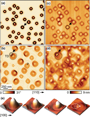
Figure 1. Three-dimensional islands resulting from Stranski–Krastanov growth processes. (a) Pyramid and dome islands obtained by deposition of 0.8 nm of Ge on Si(001) at 560°C (320 × 320 nm2, vertical scale 19 nm, image courtesy of C. Manzano. (b) Strained, intermediate and ripened islands obtained by deposition of 5.4 nm of Ge on Si(111) at 500°C (3 × 3 µm2, vertical scale 29 nm, image courtesy of N. Motta, adapted from Citation44.
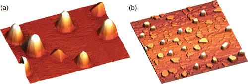
Figure 2. Average coordination numbers for Ge–Ge and Ge–Si bonds as measured by X-ray absorption spectroscopy. The results are displayed as a function of the amount of Ge deposited on Si(001) at 600°C Citation50. Reprinted with permission from F. Boscherini, G. Capellini, L. Di Gaspare, F. Rosei, N. Motta, S. Mobilio, Appl. Phys. Lett. 76, 682 (2000). Copyright 2000, American Institute of Physics.
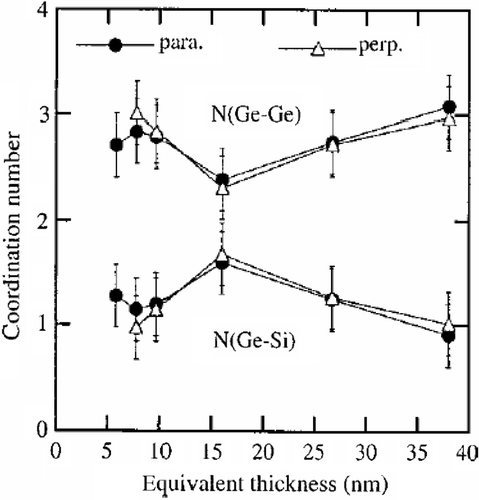
Figure 3. (a) Composition maps and (b) corresponding elastic energy maps for Ge dome islands grown on Si(001) by (A) CVD at 600°C, (B) MBE at 700°C (image courtesy of G. Medeiros-Ribeiro, adapted from Citation23)
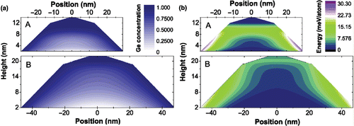
Figure 4. Computed z component of the strain tensor 2 nm below a sharp Ge–Si interface, in the region under a dome (left panel) and a pyramid (right panel) Citation65. Reprinted with permission from P. Raiteri, L. Miglio, F. Valentinotti, M. Celino, Appl. Phys. Lett. 80, 3736 (2002). Copyright 2002, American Institute of Physics.
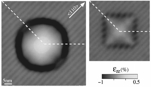
Figure 5. (a) Stress and (b) composition profile of a dome island before and after alloying respectively (adapted from Citation60). Reprinted with permission from G. Hadjisavvas, P.C. Kelires, Phys. Rev. B, 72, 75334 (2005). Copyright 2005 by the American Physical Society.
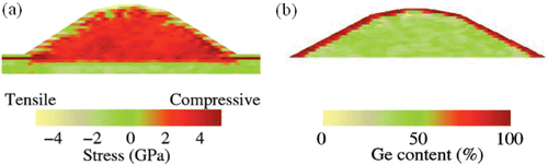
Figure 6. (a) Si content at the surface of a typical Ge/Si(111) nanostructure grown at 450°C; (b) low-energy electron microscopy image of the island in (a), displaying its faceted morphology; (c) and (d) relevant Si2p and Ge3d micrographs used for computing (a) Citation26.
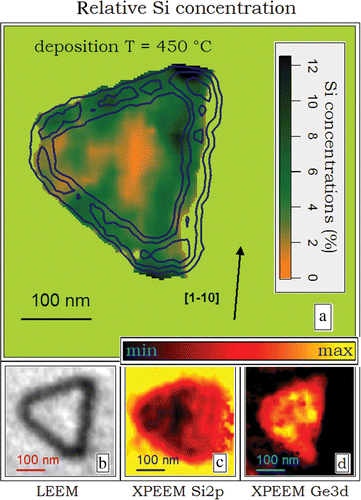
Figure 7. AFM images of Ge/Si(001) samples before (left column) and after (right column) the selective etching process. The growth temperatures are 580°C, 600°C and 620°C for the upper, central and lower row, respectively. The insets show a higher magnification (80 × 80 nm2) of the observed etched morphologies. The two different types of etched pyramids in (d) are attributed to the locally non-uniform distribution and density of the islands Citation35. Reprinted with permission from G. Katsaros, G. Costantini, M. Stoffel, R. Esteban, A.M. Bittner, A. Rastelli, U. Denker, O.G. Schmidt, K. Kern, Phys. Rev. B 72, 195320 (2005). Copyright 2005 by the American Physical Society.
Figure 8. Island shape and composition map of an axisymmetric Ge prepyramid on Si(001). Width r, height Z and composition (contour plot) are represented in scaled units. Colour code: bright regions are Si-rich, dark ones are Ge-rich Citation94. Reprinted with permission from B.J. Spencer, M. Blanariu, Phys. Rev. Lett. 95, 206101 (2005). Copyright 2005 by the American Physical Society.
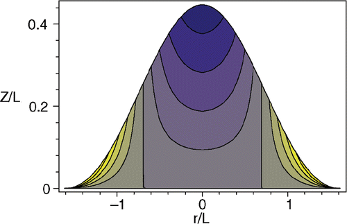
Figure 9. Simulated (left column) and measured (right column) 65% Ge isocompositional surface profiles of islands grown at increasing substrate temperatures (adapted from Citation35).
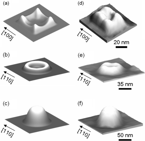
Figure 10. Representative AFM images of SiGe islands before (a), (b) and after selective removal of the SiGe layer (c), (d) of samples with 10 ML Ge grown at 740°C. In (a), (c) the surface was cooled to room temperature immediately after growth. In (b), (d) the sample was subject to a further annealing for 20 min at 740°C. (e) AFM images (440 × 440 nm2) of a SiGe island annealed for 10 minutes at 740°C (left side) and etched in NH4OH:H2O2 for (from left to right) 80 min, 170 min, and 620 min (adapted from Citation78).