Figures & data
Figure 1. SIMS profiles for samples with gate oxidation.
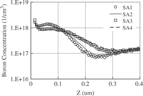
Table 1. Samples used to study segregation during gate oxidation.
Figure 2. Doping concentration of PMOS transistor constructed by 2-D process simulation.
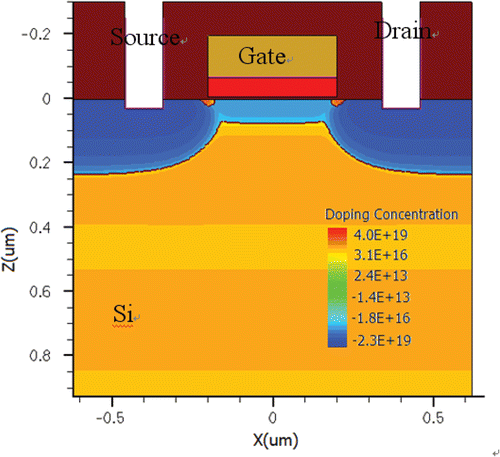
Figure 3. Id-Vg profiles of SA3 (NO annealed gate dielectric) sample for LVN and LVP transistor. Length dependency is shown well fitted due to the calibration of process simulation parameters.
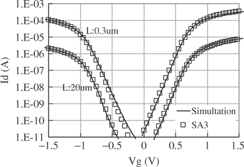
Figure 4. SIMS profile of SA3 sample and calibrated simulation result near Si/SiO2 interface.
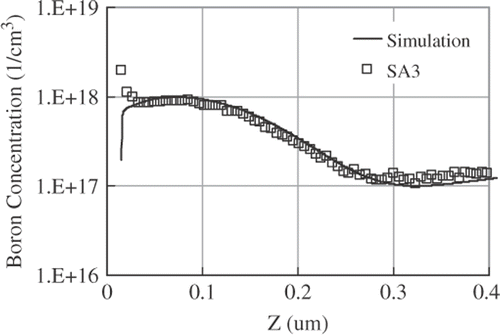
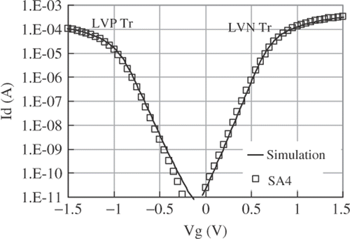
Figure 5. Id-Vg profiles for LVN and LVP transistor. SA4 sample (plasma nitrided gate dielectric) possesses 0.1 V lower VTH value than SA3 sample.
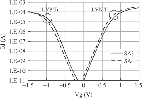
Figure 6. C-V profiles of surface channel NMOS and buried channel PMOS capacitors with different gate oxidation conditions. Buried channel PMOS capacitor of SA4 exhibits uncommon shape near Vg = 0 V.
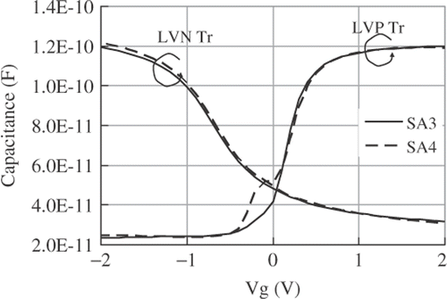
Figure 7. C-V profile for buried channel PMOS capacitor with SA4 sample and calibrated simulation result. Nit value equals 9E11 which is three times higher than that of SA3 sample.
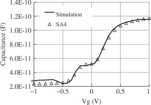
Figure 8. Id-Vg profiles for surface channel NMOS and buried channel PMOS transistor of SA4 sample. Simulation results with NIT value of 9E11 show good agreement with experiments.