Figures & data
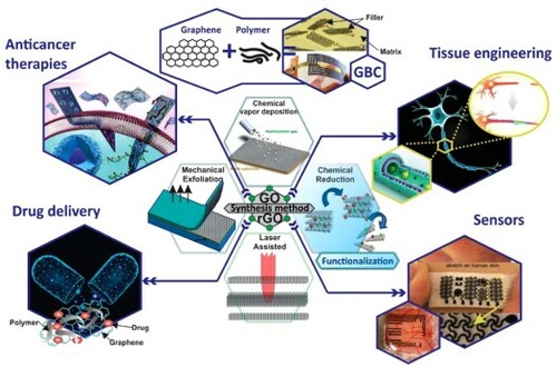
Figure 1. Typical graphene structure and their variants.
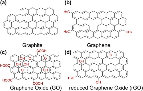
Figure 2. Hybrid graphene/Fe3O4 composites made by solvothermal reaction at 180°C. (A,B,C) TEM analysis of hybrid graphene/Fe3O4 composites made by solvothermal reaction at 4, 8, and 16 h, respectively; (D) HRTEM vision of boxed region of (C); (E, F) the subsequent SAED pattern and conventional EDS pattern of the hybrid composite graphene/Fe3O4. Reprinted from (Citation13) © 1999, the Royal Society of Chemistry.
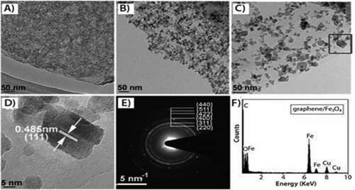
Figure 3. N-doped TiO2/graphene nano composite prepared at 180°C at varying reaction times of 7 h, 14 h, 21 h, respectively; (A, B, C), HRTEM micrograph (D), SAED pattern (E); and typical EDX pattern of N-doped TiO2 (F). Reprinted from (Citation15) © 1999, the Royal Society of Chemistry.
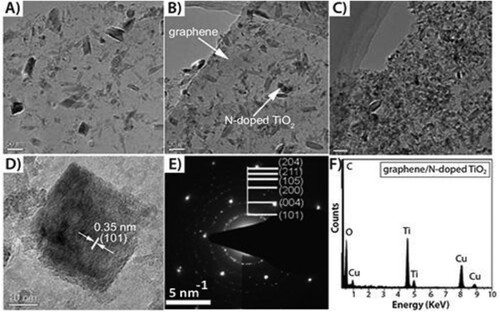
Figure 4. Different techniques of graphene producing. (a) Epitaxial growth; (b) chemical exfoliation; (c) chemical vapor deposition; (d) mechanical exfoliation; and (e) laser-assisted. Adapted from (Citation20) © 2012, Elsevier.
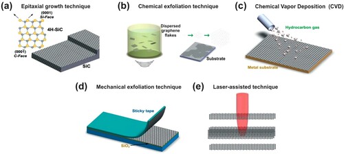
Figure 5. Schematic diagram showing expatial growth of graphene. Adapted from open access publication (Citation23) © 2018, MDPI.
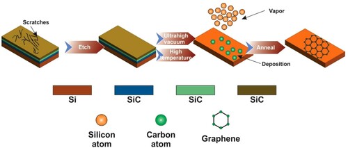
Figure 6. Schematic presentation of GBCs applications as biomaterials.
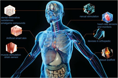
Figure 7. Schematic diagram showing graphene properties and its applications in biomedical. Adapted from open access publication (Citation16) © 2020, Taylor & Francis.
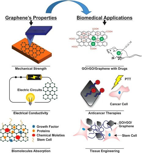
Figure 8. Potential application of GBCs as sensors for the medical field. (a) GB sensors for nervous system: schematic of graphene transistor (left) and their correspondent implant; (b) GB metabolic sensor; (c) GB bioelectrical electrode; (d) GB strain sensor; (e) GB sensor for nervous system: comparison between neural response to electrical stimulation with platinum and graphene electrode; (f) invasive sensor: The difference between tumor image captured with camera of the endoscope through metalelectronic devices (right) and transparent bioelectronic devices based on graphene (left). Adapted from open access publication (Citation111) © 2019, Frontiers.
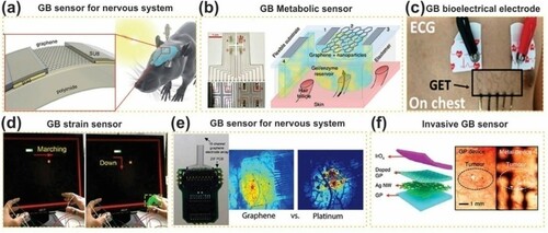
Figure 9. Graphene hybrid nanostructures for neuro-regenerative medicine. (a) Experimental substrates and (b) enhanced growth and alignment on GO-nanoparticle structure. Reprinted from (Citation121) © 2013, Wiley.
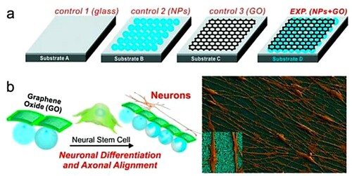
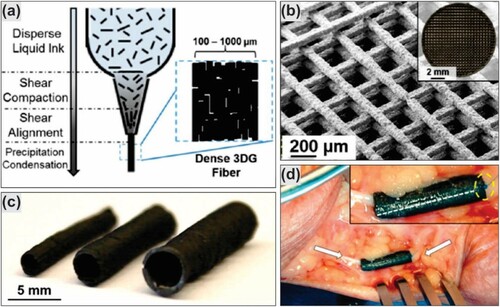
Figure 10. 3D graphene ink printed nerve conduits: (a) 3D graphene ink printed process; (b) SEM and optical (inset) images of graphene-PGA 3D printed; (c) uniaxial multichannel nerve guide of different size; and (d) nerve conduit of 3D graphene ink implanted in human cadaver. Reproduced with permission from (Citation129) © 2015, American Chemical Society.