
Figures & data
Figure 1. Freeform fabrication of robotic and shape-changing devices using smart polymeric materials: (a1) fused-filament fabrication (3D printing) of IPMC soft crawling robot, (a2) locomotion of 3D-printed IPMC-based crawling robot, and (a3) photo of 3D-printed IPMC-based crawling robot crawling along a tube; (b1) fabrication of an ionogel-based crawling robot, (b2) locomotion of an ionogel-based crawling robot, (b3) photo of an ionogel-based crawling robot crawling along a PDMS substrate; (c1) micro-projection stereolithographic (µSLA) fabrication of a SMP based flower, (c2) restoration of SMP flowers unstrained shape in response to heat, and (c3) picture of SMP flower in its unstrained shape; (d1) inkjet printing and micromachining of a phototropic liquid crystal elastomer (LCE) based artificial cilia array, (d2) actuation cycle of LCE based artificial cilia array in response to visible and UV light, and (d3) picture of actuating LCE based artificial cilia array exhibiting fast response time. Figures (a1)-(a3) adapted with permission from [Citation11]. Figures (b1)-(b3) adapted with permission from [Citation7]. Figures (c1)-(c3) adapted with permission from [Citation9]. Figures (d1)-(d3) adapted with permission from [Citation6].
![Figure 1. Freeform fabrication of robotic and shape-changing devices using smart polymeric materials: (a1) fused-filament fabrication (3D printing) of IPMC soft crawling robot, (a2) locomotion of 3D-printed IPMC-based crawling robot, and (a3) photo of 3D-printed IPMC-based crawling robot crawling along a tube; (b1) fabrication of an ionogel-based crawling robot, (b2) locomotion of an ionogel-based crawling robot, (b3) photo of an ionogel-based crawling robot crawling along a PDMS substrate; (c1) micro-projection stereolithographic (µSLA) fabrication of a SMP based flower, (c2) restoration of SMP flowers unstrained shape in response to heat, and (c3) picture of SMP flower in its unstrained shape; (d1) inkjet printing and micromachining of a phototropic liquid crystal elastomer (LCE) based artificial cilia array, (d2) actuation cycle of LCE based artificial cilia array in response to visible and UV light, and (d3) picture of actuating LCE based artificial cilia array exhibiting fast response time. Figures (a1)-(a3) adapted with permission from [Citation11]. Figures (b1)-(b3) adapted with permission from [Citation7]. Figures (c1)-(c3) adapted with permission from [Citation9]. Figures (d1)-(d3) adapted with permission from [Citation6].](/cms/asset/71cadfb6-dedf-4ee7-9c6d-66791aab21de/tsnm_a_1438534_f0001_c.jpg)
Figure 2. Structure and mechanics of actuation of IPMCs: (a) IPMC composed of platinum electrodes and a Nafion ionomer, (b) molecular composition of Nafion in its acid form (with H+ neutralized end groups), (c) IPMCs, exhibiting even distribution of hydrated cations within the ion-exchange membrane and (d) response of a hydrated IPMC to an applied voltage across its electrodes, exhibiting the migration of hydrated cations towards the cathode and a resulting bending towards the anode. Figures (a) and (b) taken with permission from [Citation222].
![Figure 2. Structure and mechanics of actuation of IPMCs: (a) IPMC composed of platinum electrodes and a Nafion ionomer, (b) molecular composition of Nafion in its acid form (with H+ neutralized end groups), (c) IPMCs, exhibiting even distribution of hydrated cations within the ion-exchange membrane and (d) response of a hydrated IPMC to an applied voltage across its electrodes, exhibiting the migration of hydrated cations towards the cathode and a resulting bending towards the anode. Figures (a) and (b) taken with permission from [Citation222].](/cms/asset/8f77a746-8a39-44b5-859e-11da9853ba6c/tsnm_a_1438534_f0002_c.jpg)
Table 1. Ion exchange/poly-electrolyte materials for use in ionic polymer metal composites and other ionic polymer actuators. All values pertain to the acid(H+) form unless specified differently. Costs are from Sigma-Aldrich.
Figure 3. Methods of shaping ionomeric materials such as Nafion: (a1) heat and pressure are used to fuse Nafion membranes together (hot pressing), (a2) ion-exchange material is pressed into a heated mold, (b1) solvents are evaporated out of Nafion dispersions in a vacuum oven (dispersion recasting), (b2) dispersion is patterned onto the surface of a material using a stencil, (c1) freeform fabrication of IPMCs using dispersions of ionomeric material cast into a 3D-printed silicone mold and fused filament fabrication of precursor to ion-exchange material. Figure (a2) reprinted with permission from [Citation223]. Figure (b2) reprinted with permission from [Citation224]. Figure (c1) reprinted with permission from [Citation4]. Figure (c2) reprinted with permission from [Citation11].
![Figure 3. Methods of shaping ionomeric materials such as Nafion: (a1) heat and pressure are used to fuse Nafion membranes together (hot pressing), (a2) ion-exchange material is pressed into a heated mold, (b1) solvents are evaporated out of Nafion dispersions in a vacuum oven (dispersion recasting), (b2) dispersion is patterned onto the surface of a material using a stencil, (c1) freeform fabrication of IPMCs using dispersions of ionomeric material cast into a 3D-printed silicone mold and fused filament fabrication of precursor to ion-exchange material. Figure (a2) reprinted with permission from [Citation223]. Figure (b2) reprinted with permission from [Citation224]. Figure (c1) reprinted with permission from [Citation4]. Figure (c2) reprinted with permission from [Citation11].](/cms/asset/11572b4b-c850-486a-8b0c-bbfa552335aa/tsnm_a_1438534_f0003_c.jpg)
Figure 4. Growth of ‘nanothorn’ clusters at Nafion-platinum electrode interface and improved bending performance in response to repeated chemical plating processes where Pt(n) indicates an IPMC fabricated with n number of plating processes: (a) Nafion-platinum electrode interface, (b) bending response of IPMCs to 0.1 Hz, 1 V square-wave inputs, (c) bending response of IPMCs to 0.1 Hz, 3 V square-wave inputs. Figures reprinted with permission from [Citation83].
![Figure 4. Growth of ‘nanothorn’ clusters at Nafion-platinum electrode interface and improved bending performance in response to repeated chemical plating processes where Pt(n) indicates an IPMC fabricated with n number of plating processes: (a) Nafion-platinum electrode interface, (b) bending response of IPMCs to 0.1 Hz, 1 V square-wave inputs, (c) bending response of IPMCs to 0.1 Hz, 3 V square-wave inputs. Figures reprinted with permission from [Citation83].](/cms/asset/7bc5a87a-ef25-4704-8061-b2bc70a05932/tsnm_a_1438534_f0004_c.jpg)
Figure 5. Comparison of ionic polymer actuators with conventional platinum electrodes and laser-scribed reduced graphene oxide paper: (a) conventional IPMC actuator exhibiting cracked electrodes due to fatigue and electrolyte loss through the electrode cracks, and (b) novel ionic polymer-graphene composite (IPGC) exhibiting durable electrodes and no electrolyte loss. Figure reprinted with permission from [Citation92] (Copyright 2014 American Chemical Society).
![Figure 5. Comparison of ionic polymer actuators with conventional platinum electrodes and laser-scribed reduced graphene oxide paper: (a) conventional IPMC actuator exhibiting cracked electrodes due to fatigue and electrolyte loss through the electrode cracks, and (b) novel ionic polymer-graphene composite (IPGC) exhibiting durable electrodes and no electrolyte loss. Figure reprinted with permission from [Citation92] (Copyright 2014 American Chemical Society).](/cms/asset/c3b79715-8b2c-48b8-8041-562238ab17f4/tsnm_a_1438534_f0005_c.jpg)
Figure 6. Fused-filament 3D printing for fabrication of custom-shaped IPMCs: (a1) 3D printing of custom geometry using precursor of an ion-exchange material, (a2) example structures 3D printed using precursor of an ion-exchange material (b1) functionalization of printed structures by hydrolysis with a strong base and swelling agent followed by plating of the functionalized structure by an impregnation reduction process, (b2) example custom shaped IPMCs, (c) actuation response of an example custom shaped IPMC. Figures (a2), (b2) and (c) reprinted with permission from [Citation212].
![Figure 6. Fused-filament 3D printing for fabrication of custom-shaped IPMCs: (a1) 3D printing of custom geometry using precursor of an ion-exchange material, (a2) example structures 3D printed using precursor of an ion-exchange material (b1) functionalization of printed structures by hydrolysis with a strong base and swelling agent followed by plating of the functionalized structure by an impregnation reduction process, (b2) example custom shaped IPMCs, (c) actuation response of an example custom shaped IPMC. Figures (a2), (b2) and (c) reprinted with permission from [Citation212].](/cms/asset/cecf702c-379b-4c7d-b535-42450e076b17/tsnm_a_1438534_f0006_c.jpg)
Figure 7. Conventionally assembled IPMC actuators vs. 3D-printed IPMC actuators exhibiting attenuated response of thicker 3D-printed IPMCs to 2.5 volt, 0.5 Hz periodic inputs due to longer response time and greater stiffness: (a1) actuation of linear actuator constructed from IPMC actuators and passive materials, (a2) actuation of 3D-printed linear actuator, (b1) actuation of rotary actuator constructed from IPMC actuators and passive materials, (b2) actuation of 3D-printed rotary actuator, (c1) lateral actuation of MDoF actuator constructed from IPMC actuators and passive materials, (c2) lateral actuation of 3D-printed MDoF actuator, (d1) translational actuation of MDoF actuator constructed from IPMC actuators and passive materials, (d2) translational actuation of 3D-printed MDoF actuator. Figures (a2), (b2), (c2) and (d2) reprinted with permission from [Citation212]. (a1) reprinted with permission from [Citation95]. Figure (b1) reprinted with permission from [Citation96]. (c1) and (d1) reprinted with permission from [Citation14].
![Figure 7. Conventionally assembled IPMC actuators vs. 3D-printed IPMC actuators exhibiting attenuated response of thicker 3D-printed IPMCs to 2.5 volt, 0.5 Hz periodic inputs due to longer response time and greater stiffness: (a1) actuation of linear actuator constructed from IPMC actuators and passive materials, (a2) actuation of 3D-printed linear actuator, (b1) actuation of rotary actuator constructed from IPMC actuators and passive materials, (b2) actuation of 3D-printed rotary actuator, (c1) lateral actuation of MDoF actuator constructed from IPMC actuators and passive materials, (c2) lateral actuation of 3D-printed MDoF actuator, (d1) translational actuation of MDoF actuator constructed from IPMC actuators and passive materials, (d2) translational actuation of 3D-printed MDoF actuator. Figures (a2), (b2), (c2) and (d2) reprinted with permission from [Citation212]. (a1) reprinted with permission from [Citation95]. Figure (b1) reprinted with permission from [Citation96]. (c1) and (d1) reprinted with permission from [Citation14].](/cms/asset/695f662f-1191-4745-a0cb-526080b32452/tsnm_a_1438534_f0007_c.jpg)
Figure 8. Response of 3D-printed custom-shaped monolithic actuators shown in : (a) mean response of linear actuator shown in ) to square wave inputs over ten successive cycles over a range of 0.5 to 3 volts and from 0.01 to 5 Hz, (b) mean response of rotary actuator shown in ) to square wave inputs over ten successive cycles over a range of 0.5 to 3 volts and from 0.01 to 5 Hz (c) mean response of MDoF actuator shown in ) in lateral direction to square wave inputs over ten successive cycles over a range of 0.5 to 3 volts and from 0.01 to 5 Hz to anti-phase voltage inputs, (d) mean response of MDoF actuator shown in ) in translational direction to square wave inputs over ten successive cycles over a range of 0.5 to 3 volts and from 0.01 to 5 Hz to in phase voltage inputs.
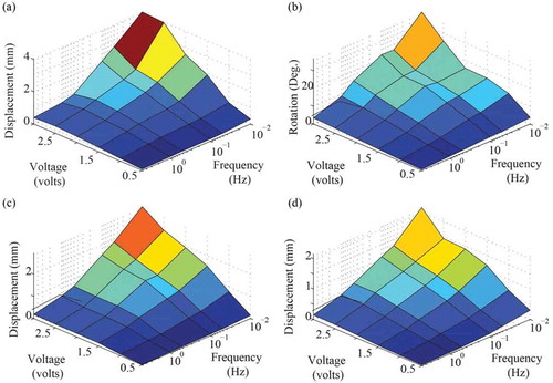
Figure 9. Successive step responses of the tip displacement of a cantilevered IPMC actuator exhibiting back-relaxation and non-repeatability. In response to a step input, a cantilevered IPMC actuator initially rises and then falls back past its initial position. A subsequent test on the same system under the same conditions also exhibits back-relaxation but the response is different than the response elicited in the first test. Figure reprinted with permission from [Citation42].
![Figure 9. Successive step responses of the tip displacement of a cantilevered IPMC actuator exhibiting back-relaxation and non-repeatability. In response to a step input, a cantilevered IPMC actuator initially rises and then falls back past its initial position. A subsequent test on the same system under the same conditions also exhibits back-relaxation but the response is different than the response elicited in the first test. Figure reprinted with permission from [Citation42].](/cms/asset/36cf8fdd-7476-4a42-91b2-a84f019c9443/tsnm_a_1438534_f0009_c.jpg)
Figure 10. Use of sectored ionic polymer-metal composite (IPMC) to address back-relaxation: (a) conceptual design of sectored IPMC actuator, (b) illustration of the cancellation effect using the responses of the independent sectors. Figure reprinted with permission from [Citation43].
![Figure 10. Use of sectored ionic polymer-metal composite (IPMC) to address back-relaxation: (a) conceptual design of sectored IPMC actuator, (b) illustration of the cancellation effect using the responses of the independent sectors. Figure reprinted with permission from [Citation43].](/cms/asset/d874b13f-fc25-4c0d-b3da-1326b2f167ac/tsnm_a_1438534_f0010_c.jpg)
Figure 11. Self-sensing IPMC actuator designs: (a) change in electrode surface resistance (R1 and R2 vs. R1′ and R2′) due to strain from IPMC bending, (b) self-sensing IPMC design using difference in voltage drop along electrodes of the constrained sections of IPMC and electrodes along the unconstrained sections of the IPMC ((UM1 – UF1) − (UM2 – UF2)), (c) IPMC sectored into three sectors consisting of actuator, shielding and sensor regions, (d) input signal into IPMC actuator in Fig. (b) consisting of actuation signal with high frequency component that can be utilized for sensing after filtering out low frequency component, (e) bridge configuration utilized with IPMC actuator in Fig. (c) for sensing. Figures (a-d) reprinted with permission from [Citation141]. Figure (e) reprinted with permission from [Citation101].
![Figure 11. Self-sensing IPMC actuator designs: (a) change in electrode surface resistance (R1 and R2 vs. R1′ and R2′) due to strain from IPMC bending, (b) self-sensing IPMC design using difference in voltage drop along electrodes of the constrained sections of IPMC and electrodes along the unconstrained sections of the IPMC ((UM1 – UF1) − (UM2 – UF2)), (c) IPMC sectored into three sectors consisting of actuator, shielding and sensor regions, (d) input signal into IPMC actuator in Fig. (b) consisting of actuation signal with high frequency component that can be utilized for sensing after filtering out low frequency component, (e) bridge configuration utilized with IPMC actuator in Fig. (c) for sensing. Figures (a-d) reprinted with permission from [Citation141]. Figure (e) reprinted with permission from [Citation101].](/cms/asset/28b654bb-2302-47bf-9cf8-95815a63ac29/tsnm_a_1438534_f0011_c.jpg)
Figure 12. IPMC actuators integrated with resistive or piezoelectric sensors: (a1) cantilevered IPMC bending actuator integrated with a strain gauge and a tube-shaped IPMC actuator integrated with nichrome wire, (a2) Wheatstone bridge circuit for use with resistive sensor like a strain gauge or nichrome wire, (b2) cantilevered IPMC bending actuator integrated with insulation and two layers of PVDF film, and (b2) differential charge amplifier circuit for use with PVDF film sensors. Figures (a1) and (a2) taken with permission from [Citation222]. Figures (b1) and (b2) reprinted with permission from [Citation101].
![Figure 12. IPMC actuators integrated with resistive or piezoelectric sensors: (a1) cantilevered IPMC bending actuator integrated with a strain gauge and a tube-shaped IPMC actuator integrated with nichrome wire, (a2) Wheatstone bridge circuit for use with resistive sensor like a strain gauge or nichrome wire, (b2) cantilevered IPMC bending actuator integrated with insulation and two layers of PVDF film, and (b2) differential charge amplifier circuit for use with PVDF film sensors. Figures (a1) and (a2) taken with permission from [Citation222]. Figures (b1) and (b2) reprinted with permission from [Citation101].](/cms/asset/8f23ff38-46a9-4604-98ae-048670d10408/tsnm_a_1438534_f0012_c.jpg)
Figure 13. Equivalent circuit models of IPMC electrical dynamics and comparison to experimentally measured impedance of an IPMC over a range of frequencies: (a) a resistor and capacitor in series, (b) a resistor and capacitor in series with a resistor added in parallel [Citation110], (c) two parallel arrangements of a resistor and a capacitor connected in series with a bulk resistor [Citation111], (d) model including eight components as well as nonlinear diodes [Citation112], (e) RC circuit with a Warburg impedance element [Citation109], (f) real part of the impedance of an IPMC compared to models, (g) imaginary part of the impedance of an IPMC compared to models. Figure adapted with permission from [Citation109].
![Figure 13. Equivalent circuit models of IPMC electrical dynamics and comparison to experimentally measured impedance of an IPMC over a range of frequencies: (a) a resistor and capacitor in series, (b) a resistor and capacitor in series with a resistor added in parallel [Citation110], (c) two parallel arrangements of a resistor and a capacitor connected in series with a bulk resistor [Citation111], (d) model including eight components as well as nonlinear diodes [Citation112], (e) RC circuit with a Warburg impedance element [Citation109], (f) real part of the impedance of an IPMC compared to models, (g) imaginary part of the impedance of an IPMC compared to models. Figure adapted with permission from [Citation109].](/cms/asset/0dee782d-ef2b-4b1a-972f-444a42c355b7/tsnm_a_1438534_f0013_c.jpg)
Figure 14. Methods for controlling IPMCs: model-based feedforward control of an IPMC that functions by determining the requisite input (uff) to produce the desired output (yd), (b) feedback control of an IPMC that uses sensor information to determine a control effort based on the error (e) between the desired output (yd) and the actual output (y), and (c) integrated feedforward/feedback control that uses feedback control to correct for disturbances and modelling error. Figure taken with permission from [Citation222].
![Figure 14. Methods for controlling IPMCs: model-based feedforward control of an IPMC that functions by determining the requisite input (uff) to produce the desired output (yd), (b) feedback control of an IPMC that uses sensor information to determine a control effort based on the error (e) between the desired output (yd) and the actual output (y), and (c) integrated feedforward/feedback control that uses feedback control to correct for disturbances and modelling error. Figure taken with permission from [Citation222].](/cms/asset/38e95d53-188d-4542-a6d3-d780080308dc/tsnm_a_1438534_f0014_b.gif)
Figure 15. Composition of conductive polymers illustrating their conjugated structure of alternating single and double bonds and the reduced and oxidized states: (a) undoped conjugated polymer (reduced), (b) doped conjugated polymer (oxidized). Figure reprinted with permission from [Citation120].
![Figure 15. Composition of conductive polymers illustrating their conjugated structure of alternating single and double bonds and the reduced and oxidized states: (a) undoped conjugated polymer (reduced), (b) doped conjugated polymer (oxidized). Figure reprinted with permission from [Citation120].](/cms/asset/e1b167b9-0269-40a3-86c1-7709432d13e9/tsnm_a_1438534_f0015_b.gif)
Figure 16. Demonstration of the difference in bending direction of ionic gels with an anionic and cationic polymer network: (a) no electric field is applied and no bending is exhibited, (b) an electric field is applied causing the cationic gel (blue) to bend toward the anode and the anionic gel (red) to bend toward the cathode.
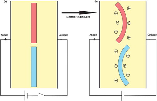
Figure 17. Illustration of a tri-layer conjugated polymer actuator demonstrating bending actuation (left) and linear actuation (right). Figure reprinted with permission from [Citation225].
![Figure 17. Illustration of a tri-layer conjugated polymer actuator demonstrating bending actuation (left) and linear actuation (right). Figure reprinted with permission from [Citation225].](/cms/asset/88eb158e-3306-410e-87d5-a9a359c24392/tsnm_a_1438534_f0017_c.jpg)
Figure 18. Applications of conductive polymerbi-layer actuators: (a) robot for handling microscopic glass beads, (b) cell clinic with an active hinge. Figure (a) reprinted with permission from [Citation2]. Figure (b) reprinted with permission from [Citation3].
![Figure 18. Applications of conductive polymerbi-layer actuators: (a) robot for handling microscopic glass beads, (b) cell clinic with an active hinge. Figure (a) reprinted with permission from [Citation2]. Figure (b) reprinted with permission from [Citation3].](/cms/asset/e3453280-1e6d-4a33-8aca-3ffb48a3b29b/tsnm_a_1438534_f0018_c.jpg)
Figure 19. Applications of ionic gels: (a) walking robot fabricated by laser cutting prefabricated ionic gels, (b) multi-stimuli responsive micro-robots fabricated using a microfluidic device and photo-lithographic techniques. Figure (a) reprinted with permission from [Citation7]. Figure (b) reprinted with permission from [Citation5].
![Figure 19. Applications of ionic gels: (a) walking robot fabricated by laser cutting prefabricated ionic gels, (b) multi-stimuli responsive micro-robots fabricated using a microfluidic device and photo-lithographic techniques. Figure (a) reprinted with permission from [Citation7]. Figure (b) reprinted with permission from [Citation5].](/cms/asset/0082f206-1f86-47b9-a225-dee3ad9e722e/tsnm_a_1438534_f0019_c.jpg)
Figure 20. Deposition of conjugated polymer film: (a) from spin coating a dispersion of the conjugated polymer (b) spin coating a precursor of the conjugated polymer, followed by curing, (c) vapor deposition, (d) electro-polymerization. Figure reprinted with permission from [Citation129].
![Figure 20. Deposition of conjugated polymer film: (a) from spin coating a dispersion of the conjugated polymer (b) spin coating a precursor of the conjugated polymer, followed by curing, (c) vapor deposition, (d) electro-polymerization. Figure reprinted with permission from [Citation129].](/cms/asset/a4715c3b-2797-49bf-bc9d-fe746b76d100/tsnm_a_1438534_f0020_b.gif)
Figure 21. In situ polymerization of vinyl monomers dissolved in an ionic liquid to produce an ionic gel. Figure reprinted with permission from [Citation131] (Copyright 2009 American Chemical Society).
![Figure 21. In situ polymerization of vinyl monomers dissolved in an ionic liquid to produce an ionic gel. Figure reprinted with permission from [Citation131] (Copyright 2009 American Chemical Society).](/cms/asset/19c0faaa-9d8c-4427-9bdd-11f744f3d019/tsnm_a_1438534_f0021_c.jpg)
Figure 22. Composition of a ‘bucky-gel’ actuator: (a) schematic of layered structure of bucky-gel actuator consisting of a ionic gel with single wall nanotubes (SMNT)s as the electrode layer and a pristine ionic gel as the polyelectrolyte layer sandwiched between the electrode layers, (b) chemical formula of the ionic liquid, 1-butyl-3-methylimidazolium tetrafluoroborate (BMIBF4), and the polymer, poly(vinylidene fluoride-co-hexafluoropropylene) (PVdF(HFP). Figure reprinted with permission from [Citation136].
![Figure 22. Composition of a ‘bucky-gel’ actuator: (a) schematic of layered structure of bucky-gel actuator consisting of a ionic gel with single wall nanotubes (SMNT)s as the electrode layer and a pristine ionic gel as the polyelectrolyte layer sandwiched between the electrode layers, (b) chemical formula of the ionic liquid, 1-butyl-3-methylimidazolium tetrafluoroborate (BMIBF4), and the polymer, poly(vinylidene fluoride-co-hexafluoropropylene) (PVdF(HFP). Figure reprinted with permission from [Citation136].](/cms/asset/88fb8f5f-6250-401e-876c-88db246401df/tsnm_a_1438534_f0022_c.jpg)
Figure 23. Micromachining methods of patterning conjugated polymers and electrodes: (a) direct patterning of conjugated polymer using UV light and a mask, (b) deposition of conjugated polymer onto selectively patterned electrodes, (c) selective deposition of conjugated polymer using etched photo resist, (d) etching of deposited conjugated polymer layer after being deposited, (e) selectively removing conductivity of conjugated polymer, (f) selective doping of conjugated polymer. Figure reprinted with permission from [Citation129].
![Figure 23. Micromachining methods of patterning conjugated polymers and electrodes: (a) direct patterning of conjugated polymer using UV light and a mask, (b) deposition of conjugated polymer onto selectively patterned electrodes, (c) selective deposition of conjugated polymer using etched photo resist, (d) etching of deposited conjugated polymer layer after being deposited, (e) selectively removing conductivity of conjugated polymer, (f) selective doping of conjugated polymer. Figure reprinted with permission from [Citation129].](/cms/asset/27128fa0-7072-4f3c-9d10-54c53e426824/tsnm_a_1438534_f0023_b.gif)
Figure 24. Micromachining methods of creating out of plane conjugated polymer bending actuators: (a) use of a sacrificial layer (b) differential adhesion method. Figure reprinted with permission from [Citation129].
![Figure 24. Micromachining methods of creating out of plane conjugated polymer bending actuators: (a) use of a sacrificial layer (b) differential adhesion method. Figure reprinted with permission from [Citation129].](/cms/asset/011f3cf4-aa4b-4796-bdf4-6034aa2a338e/tsnm_a_1438534_f0024_b.gif)
Figure 25. Freeform fabrication of ionic gel robots and devices: (a1) use of a microfluidic device and photo-polymerization using an ultraviolet (UV) light and photo-mask to selectively cure solutions of monomers and ionic liquids to sequentially fabricate miniature ionogels, (a2) a biomimetic aqua-bot fabricated using this technique, (b1) laser-cutting device components out of prefabricated ionogel material, (b2) a walking robot fabricated using this laser cutting technique. Figures (a1) and (a2) adapted with permission from [Citation5]. Figures (b1) and (b2) adapted with permission from [Citation7].
![Figure 25. Freeform fabrication of ionic gel robots and devices: (a1) use of a microfluidic device and photo-polymerization using an ultraviolet (UV) light and photo-mask to selectively cure solutions of monomers and ionic liquids to sequentially fabricate miniature ionogels, (a2) a biomimetic aqua-bot fabricated using this technique, (b1) laser-cutting device components out of prefabricated ionogel material, (b2) a walking robot fabricated using this laser cutting technique. Figures (a1) and (a2) adapted with permission from [Citation5]. Figures (b1) and (b2) adapted with permission from [Citation7].](/cms/asset/53aeb933-5e77-46a0-98ca-3197cb598e91/tsnm_a_1438534_f0025_c.jpg)
Figure 26. Proposed self-sensing feedback control of a tri-layer polymer bending actuator: (a) schematic of tri-layer polymer bending actuator with a groove cut in the conjugated polymer that acts as the electrode to electrically isolate the actuator from the sensor region, (b) proposed control method utilizing the inverse dynamics of the sensor. Figure reprinted with permission from [Citation140].
![Figure 26. Proposed self-sensing feedback control of a tri-layer polymer bending actuator: (a) schematic of tri-layer polymer bending actuator with a groove cut in the conjugated polymer that acts as the electrode to electrically isolate the actuator from the sensor region, (b) proposed control method utilizing the inverse dynamics of the sensor. Figure reprinted with permission from [Citation140].](/cms/asset/5b436fdd-2f9b-4bc5-880d-fbd3a4ff3cd2/tsnm_a_1438534_f0026_c.jpg)
Figure 27. Cycle of ‘programming’ a thermal active SMP with a deformed shape and then restoring its undeformed shape through the following steps: (1) straining the material by applying a mechanical load, (2) cooling the material to ‘freeze’ in the deformed shape, (3) unloading the material, and finally (4) heating the material to restore its undeformed shape. Figure adapted with permission from [Citation226].
![Figure 27. Cycle of ‘programming’ a thermal active SMP with a deformed shape and then restoring its undeformed shape through the following steps: (1) straining the material by applying a mechanical load, (2) cooling the material to ‘freeze’ in the deformed shape, (3) unloading the material, and finally (4) heating the material to restore its undeformed shape. Figure adapted with permission from [Citation226].](/cms/asset/6ffb7975-9e83-4894-b6ae-08b1f78ce3eb/tsnm_a_1438534_f0027_c.jpg)
Figure 28. Photo-fixing and photo-cleaving of light responsive SMP through irradiation with light of appropriate wavelengths. The chromophores (open triangles) are covalently grafted onto the permanent polymer network, forming photoreversible cross-links (filled diamonds). The SMP is ‘programed’ with a deformed shaped by irradiating it with light of a suitable wavelength. The undeformed shape is restored by irradiating the polymer with light of a different wavelength. Figure reprinted with permission from [Citation163].
![Figure 28. Photo-fixing and photo-cleaving of light responsive SMP through irradiation with light of appropriate wavelengths. The chromophores (open triangles) are covalently grafted onto the permanent polymer network, forming photoreversible cross-links (filled diamonds). The SMP is ‘programed’ with a deformed shaped by irradiating it with light of a suitable wavelength. The undeformed shape is restored by irradiating the polymer with light of a different wavelength. Figure reprinted with permission from [Citation163].](/cms/asset/43a0164a-0373-4294-806a-c8e27f0a9519/tsnm_a_1438534_f0028_b.gif)
Figure 29. Projection micro-stereolithographic printing of a multi-material SMP: (a) Process of fabricating multi-material monolithic structure, (b) Photo-curable shape memory polymer network constructed using mono-functional monomer, Benzyl methacrylate (BMA) as linear chain builder (LCB), and multi-functional oligomers, Poly (ethylene glycol) dimethacrylate (PEGDMA), Bisphenol A ethoxylate dimethacrylate (BPA), and Di(ethylene glycol) dimethacrylate (DEGDMA) as crosslinkers. Figure adapted with permission from [Citation166].
![Figure 29. Projection micro-stereolithographic printing of a multi-material SMP: (a) Process of fabricating multi-material monolithic structure, (b) Photo-curable shape memory polymer network constructed using mono-functional monomer, Benzyl methacrylate (BMA) as linear chain builder (LCB), and multi-functional oligomers, Poly (ethylene glycol) dimethacrylate (PEGDMA), Bisphenol A ethoxylate dimethacrylate (BPA), and Di(ethylene glycol) dimethacrylate (DEGDMA) as crosslinkers. Figure adapted with permission from [Citation166].](/cms/asset/16d4a017-c92f-44f2-9b2f-a23bfdec337f/tsnm_a_1438534_f0029_c.jpg)
Figure 30. Self-folding using SMPs: (a) fabrication of self-folding element consisting of PVC (SMP material), adhesive and supporting layers, (b) architecture and activation of self-folding element, (c) fold pattern of self-folding origami robot, (d) folded origami robot. Figure reprinted with permission from [Citation167].
![Figure 30. Self-folding using SMPs: (a) fabrication of self-folding element consisting of PVC (SMP material), adhesive and supporting layers, (b) architecture and activation of self-folding element, (c) fold pattern of self-folding origami robot, (d) folded origami robot. Figure reprinted with permission from [Citation167].](/cms/asset/8c457f71-8e49-4314-8bab-fb4f57342a3e/tsnm_a_1438534_f0030_c.jpg)
Figure 31. Restoration of the undeformed shape of a 3D-printed, light-triggered, thermal-responsive SMP: (a) in response to an 87 mW cm2 light source and (b) in respnse to sunlight. Note that the largest material displacement occurred between 0 and 40s and that the amount of displacement decreased in each subsequent time frame. Images reprinted with permission from [Citation165].
![Figure 31. Restoration of the undeformed shape of a 3D-printed, light-triggered, thermal-responsive SMP: (a) in response to an 87 mW cm2 light source and (b) in respnse to sunlight. Note that the largest material displacement occurred between 0 and 40s and that the amount of displacement decreased in each subsequent time frame. Images reprinted with permission from [Citation165].](/cms/asset/97437485-e3ef-40b5-870d-b6102d57ddd6/tsnm_a_1438534_f0031_c.jpg)
Figure 32. The SMP film actuator presented in [Citation165]. An image of the 3D-printed film is shown in (a) and (b). The illumination time versus deformation angle for varying film thicknesses are shown in (c). The illumination time versus deformation angle with varying light intensities are shown in (d). Finally, the three axis graph of the illumination time versus light intensity versus deformation angle is shown in (e). Figure reprinted with permission from [Citation165].
![Figure 32. The SMP film actuator presented in [Citation165]. An image of the 3D-printed film is shown in (a) and (b). The illumination time versus deformation angle for varying film thicknesses are shown in (c). The illumination time versus deformation angle with varying light intensities are shown in (d). Finally, the three axis graph of the illumination time versus light intensity versus deformation angle is shown in (e). Figure reprinted with permission from [Citation165].](/cms/asset/189b25f2-5c2f-49b2-ae7d-80ee9d6db8fe/tsnm_a_1438534_f0032_c.jpg)
Figure 33. Liquid crystal polymers: (a1) smectic A liquid crystal phase exhibiting alignment and layers, (a2) smectic C liquid crystal phase exhibiting alignment and layers, (a3) nematic liquid crystal phase exhibiting alignment and but not layers, (a4) isotropic phase exhibiting neither alignment nor layers, (b1) main chain liquid crystal polymer with mesogenic groups incorporated into backbone polymer, (b2) side-on liquid crystal polymer with mesogenic groups side linked to backbone, (b3) end-on liquid crystal polymer with mesogenic group end linked to backbone, (c1) cross-linking of a liquid crystal network (LCN), (c2) cross-linking of a liquid crystal elastomer (LCE), (d1) representative linear LCP, with melting temp in excess of 300◦ C, elastic modulus in excess of 100 GPa and minimal change in entropy in response to stimuli, (d2) representative liquid crystal network with a glass transition temperature of 40–120◦ C, an elastic modulus of 0.8–2 GPa and a change in entropy of about 5%, representative liquid crystal elastomer with a glass transition temperature of less than 20◦ C, an elastic modulus of between 0.1–5 MPa and a change in entropy in excess of 90% [Citation1,Citation29]. Figures (d1)-(d3) reprinted with permission from [Citation29].
![Figure 33. Liquid crystal polymers: (a1) smectic A liquid crystal phase exhibiting alignment and layers, (a2) smectic C liquid crystal phase exhibiting alignment and layers, (a3) nematic liquid crystal phase exhibiting alignment and but not layers, (a4) isotropic phase exhibiting neither alignment nor layers, (b1) main chain liquid crystal polymer with mesogenic groups incorporated into backbone polymer, (b2) side-on liquid crystal polymer with mesogenic groups side linked to backbone, (b3) end-on liquid crystal polymer with mesogenic group end linked to backbone, (c1) cross-linking of a liquid crystal network (LCN), (c2) cross-linking of a liquid crystal elastomer (LCE), (d1) representative linear LCP, with melting temp in excess of 300◦ C, elastic modulus in excess of 100 GPa and minimal change in entropy in response to stimuli, (d2) representative liquid crystal network with a glass transition temperature of 40–120◦ C, an elastic modulus of 0.8–2 GPa and a change in entropy of about 5%, representative liquid crystal elastomer with a glass transition temperature of less than 20◦ C, an elastic modulus of between 0.1–5 MPa and a change in entropy in excess of 90% [Citation1,Citation29]. Figures (d1)-(d3) reprinted with permission from [Citation29].](/cms/asset/722c1862-e7ec-4745-916e-077d173e4fa5/tsnm_a_1438534_f0033_c.jpg)
Figure 34. Macroscopic shape changes in liquid crystal polymers resultant from various mesogen structures: (a) planar uniaxial shape change resultant from isomerization of corresponding mesogen structure, (b) cholesteric shape change resultant from isomerization of corresponding mesogen structure, (c) twisted nematic shape change resultant from isomerization of corresponding mesogen structure, (d) splay-bend shape change resultant from isomerization of corresponding mesogen structure. Figure reprinted with permission from [Citation29].
![Figure 34. Macroscopic shape changes in liquid crystal polymers resultant from various mesogen structures: (a) planar uniaxial shape change resultant from isomerization of corresponding mesogen structure, (b) cholesteric shape change resultant from isomerization of corresponding mesogen structure, (c) twisted nematic shape change resultant from isomerization of corresponding mesogen structure, (d) splay-bend shape change resultant from isomerization of corresponding mesogen structure. Figure reprinted with permission from [Citation29].](/cms/asset/c4db6668-9f31-4380-a6ab-bec363042b31/tsnm_a_1438534_f0034_c.jpg)
Figure 35. Applications of liquid crystal elastomers (LCE): (a1) anisotropic shape change of thermotropic LCE in response to change in temperature, (a2) thermotropic LCE lifting a weight in response to heating, (a3) dimensional changes of thermotropic LCE in response to heating where L is the original length, Liso is the heated (isotropic length) and Lper is the width (length perpendicular) of the thermotropic LCE, (b1) diagram of peristaltic locomotion of a phototropic LCE worm-like robot using structured light, (b2) photos of the locomotion sequence of a phototropic LCE worm-like robot using structured light, (c1) diagram of ray- like swimming of a phototropic LCE using structured light, (c2) photos of the locomotion sequence of a phototropic LCE using structured light. Figures (a1)-(a3) reprinted with permission from [Citation29]. Figures (b1) and (b2) reprinted with permission from [Citation182]. Figures (c1) and (c2) reprinted with permission from [Citation183].
![Figure 35. Applications of liquid crystal elastomers (LCE): (a1) anisotropic shape change of thermotropic LCE in response to change in temperature, (a2) thermotropic LCE lifting a weight in response to heating, (a3) dimensional changes of thermotropic LCE in response to heating where L is the original length, Liso is the heated (isotropic length) and Lper is the width (length perpendicular) of the thermotropic LCE, (b1) diagram of peristaltic locomotion of a phototropic LCE worm-like robot using structured light, (b2) photos of the locomotion sequence of a phototropic LCE worm-like robot using structured light, (c1) diagram of ray- like swimming of a phototropic LCE using structured light, (c2) photos of the locomotion sequence of a phototropic LCE using structured light. Figures (a1)-(a3) reprinted with permission from [Citation29]. Figures (b1) and (b2) reprinted with permission from [Citation182]. Figures (c1) and (c2) reprinted with permission from [Citation183].](/cms/asset/9fa3f899-5abd-4399-8ff2-cdc64bca1518/tsnm_a_1438534_f0035_c.jpg)
Figure 36. Applications of splay bend LCN bending actuators: (a) illustration of the bending deformation that results from activation of the LCN, (b1) response of a thermotropic LCN bending actuator to changing temperature, (b2) diagrams of a gripper using a thermotropic LCN for handling of silicone wafers, (b3) pictures of a gripper using a thermotropic LCN for handling of silicone wafers, (c1) response of a composite phototropic LCN bending actuator in response to visible and ultraviolet (UV) light, (c2) diagrams of artificial cilia array composed of composite phototropic LCN bending actuators, (c3) pictures of artificial cilia array composed of composite phototropic LCN bending actuators. Figures (a) and (b1)-(b3) reprinted with permission from [Citation184]. Figures (c1)-(c3) reprinted with permission from [Citation6].
![Figure 36. Applications of splay bend LCN bending actuators: (a) illustration of the bending deformation that results from activation of the LCN, (b1) response of a thermotropic LCN bending actuator to changing temperature, (b2) diagrams of a gripper using a thermotropic LCN for handling of silicone wafers, (b3) pictures of a gripper using a thermotropic LCN for handling of silicone wafers, (c1) response of a composite phototropic LCN bending actuator in response to visible and ultraviolet (UV) light, (c2) diagrams of artificial cilia array composed of composite phototropic LCN bending actuators, (c3) pictures of artificial cilia array composed of composite phototropic LCN bending actuators. Figures (a) and (b1)-(b3) reprinted with permission from [Citation184]. Figures (c1)-(c3) reprinted with permission from [Citation6].](/cms/asset/deddc27d-5cb6-40e1-b39d-a4026522758b/tsnm_a_1438534_f0036_c.jpg)
Figure 37. Four routes for synthesizing LCEs: (a) ‘one-pot’ method mixing all reactants in a palladium-catalyzed reaction, (b) liquid crystal polymers are mixed with a cross-linker that react with functional groups in the polymers, (c) liquid crystal polymers already containing cross-linking groups are activated, for instance by ultraviolet (UV) light, (d) a liquid crystal monomer is mixed with a cross-linker and is then polymerized, for instance, using UV light [Citation30]. Reprinted with permission from [Citation30].
![Figure 37. Four routes for synthesizing LCEs: (a) ‘one-pot’ method mixing all reactants in a palladium-catalyzed reaction, (b) liquid crystal polymers are mixed with a cross-linker that react with functional groups in the polymers, (c) liquid crystal polymers already containing cross-linking groups are activated, for instance by ultraviolet (UV) light, (d) a liquid crystal monomer is mixed with a cross-linker and is then polymerized, for instance, using UV light [Citation30]. Reprinted with permission from [Citation30].](/cms/asset/7cfe509b-5968-4c1f-b1cd-5b65e1a4f5e2/tsnm_a_1438534_f0037_b.gif)
Figure 38. Fabrication of a liquid crystal elastomer (LCE) by a platinum catalyzed hydrosilylation reaction: (a1) reactant poly(methylhydrogensiloxane), (a2) reactant 4-but-3-enyloxybenzoic acid 4-methoxyphenyl ester mesogen side chain, (a3) reactant nematic polyether based on 1-(4-hydroxy-4-biphenyl)-2-[4- (10-undecenyloxy)phenyl]butane, end-functionalized by vinyl groups, (b) LCE product from platinum catalyzed hydrosilylation at 60◦ C. Figure reprinted with permission from [Citation23].
![Figure 38. Fabrication of a liquid crystal elastomer (LCE) by a platinum catalyzed hydrosilylation reaction: (a1) reactant poly(methylhydrogensiloxane), (a2) reactant 4-but-3-enyloxybenzoic acid 4-methoxyphenyl ester mesogen side chain, (a3) reactant nematic polyether based on 1-(4-hydroxy-4-biphenyl)-2-[4- (10-undecenyloxy)phenyl]butane, end-functionalized by vinyl groups, (b) LCE product from platinum catalyzed hydrosilylation at 60◦ C. Figure reprinted with permission from [Citation23].](/cms/asset/00bfc73b-be76-4cf8-99c6-a4c2a678f3c3/tsnm_a_1438534_f0038_b.gif)
Figure 39. Fabrication of phototropic liquid crystal network (LCN) based artificial cilia array: (a) structured deposition of polyvinyl alcohol (PVA) release layer, 1, (b) spin-coating of polyimide alignment layer, 2, followed by curing and buffing to give desired pre-tilt, (c) ink-jet deposition of mesogenic and cross-linking monomers with azobenzene dyes, 3 & 4, which are then cured, (d) dissolving the PVA release layer. Figure reprinted with permission from [Citation6].
![Figure 39. Fabrication of phototropic liquid crystal network (LCN) based artificial cilia array: (a) structured deposition of polyvinyl alcohol (PVA) release layer, 1, (b) spin-coating of polyimide alignment layer, 2, followed by curing and buffing to give desired pre-tilt, (c) ink-jet deposition of mesogenic and cross-linking monomers with azobenzene dyes, 3 & 4, which are then cured, (d) dissolving the PVA release layer. Figure reprinted with permission from [Citation6].](/cms/asset/8684c56d-c9a4-4241-bed8-55e6cefb9d87/tsnm_a_1438534_f0039_b.gif)
Figure 40. Designable shape changes in LCEs from the inclusion of topological defects: (a) topological defects in a liquid crystal elastomer, causing a 360◦ change in director orientation, (b) shape change of thermotropic LCE with nine evenly spaced topological defects, exhibiting azimuthal contraction and radial expansion resulting in peaks centered on the topological defects, (c) multi-modal shape change of a strip of thermotropic LCE resulting from combinations of up and down modes of individual defects. Figure reprinted with permission from [Citation188].
![Figure 40. Designable shape changes in LCEs from the inclusion of topological defects: (a) topological defects in a liquid crystal elastomer, causing a 360◦ change in director orientation, (b) shape change of thermotropic LCE with nine evenly spaced topological defects, exhibiting azimuthal contraction and radial expansion resulting in peaks centered on the topological defects, (c) multi-modal shape change of a strip of thermotropic LCE resulting from combinations of up and down modes of individual defects. Figure reprinted with permission from [Citation188].](/cms/asset/80929ab7-4acf-42fc-b498-40bc5b14645b/tsnm_a_1438534_f0040_c.jpg)
Figure 41. Comparison of DEAs (left) vs. PVC gel actuators (right). On top is a DEA and a PVC gel actuator with no applied DC field. On bottomis a DEA and a PVC gel actuator with an applied DC field.
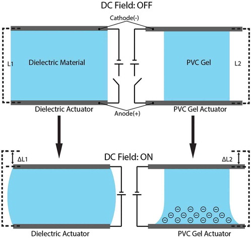
Table 2. Ionic EAP actuators. Unless otherwise stated, values are from [Citation206]. Material costs are approximate and based on pricing from commercial vendors.
Table 3. Thermal-responsive polymer actuators. Material costs are approximate and based on pricing from commercial vendors.
Figure 42. Ionic electroactive polymer actuators: (a) Conductive polymers, (b) IPMCs, (c) CNTs.
Figure 43. Thermally activated polymer actuators: (a) thermotropic LCEs, (b) thermal-responsive SMPs.
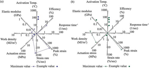
Table 4. Light-responsive smart polymeric materials.