Figures & data
Figure 1. Phase diagram of Co-Ni.[Citation12]
![Figure 1. Phase diagram of Co-Ni.[Citation12]](/cms/asset/7386b375-f761-4cbe-b52e-67b953e8f440/tmrl_a_989460_f0001_c.jpg)
Table 1. Composition of electroplating baths used in the present study.
Table 2. Pulse plating conditions leading to acceptable nanocrystalline Co-Ni deposits from saccharin-containing electrolyte.
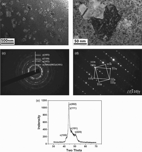
Figure 2. Initial structure (1.bright-field, 2.dark-field, 3.SAED, 4.XRD) of as-deposited samples with different nickel contents: (a) Co-20.6at%Ni; (b) Co-31.0at%Ni and (c) Co-48.0at%Ni.
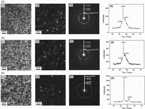
Figure 3. Typical tensile engineering stress–strain curves under a tensile rate of 0.5 mm/min: (a) free-standing sample; (b) sample together with substrate; (c) 304 stainless steel substrate and (d) curve of deposit layer estimated by ROM. The inset shows the geometry of tensile samples (R, radius of curvature).
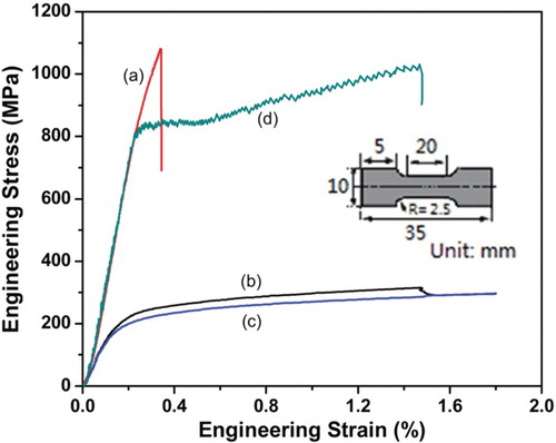
Figure 4. Bight-field TEM images of Co-31.0at%Ni after different tensile tests: (a) = 0.35% (free-standing sample); (b)
= 0.6%; (c)
= 1.0%; (d)
= 1.4% and (e)
= 1.5%.
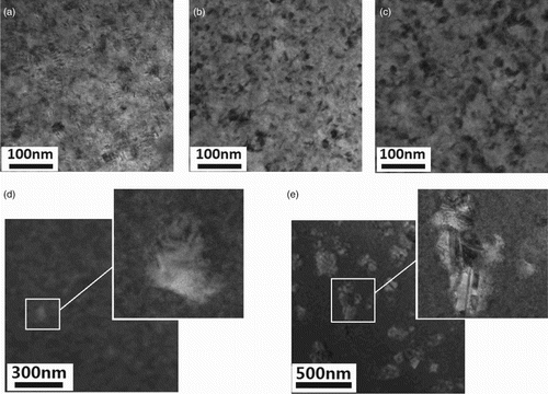
Figure 5. Structure of Co-31.0at%Ni samples after tensile failure up to = 1.5%: (a) overall bright-field image; (b) bright-field image of the grown grains; (c) SAED pattern corresponding to the background; (d) SAED pattern corresponding to the grains grown up, which is measured by nano-beam diffraction (NBD) model and (e) X-ray diffraction pattern.