Figures & data
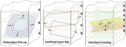
Figure 1. Predominant deformation mechanisms in laminated A/B composites: dislocation pile-up, confined layer slip, and interface crossing, with respect to layer thickness. Arrows indicate the motion direction of dislocations.
Figure 2. The crystallography of slip across interface: (a) general case, (b) parallel slip systems case, and (c) twin-oriented case. The arrows indicate the glide direction of lattice dislocations under compression normal to the interface.
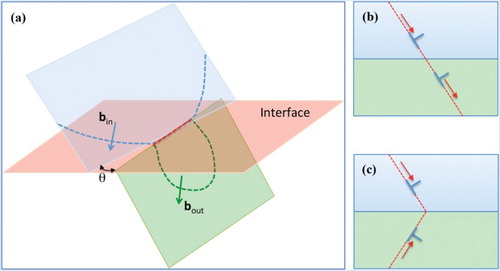
Figure 3. Maximum strength of nanolaminated materials with respect to the combination of constituent phases: (a) metal–metal crystalline laminates (b) metal-crystalline hard phase laminates, and (c) metal-metallic glass laminates. Black squares indicate the strength of constituent 1 under the black line and red circles represent the strength of constituent 2 above the black line in the horizontal axis. Blue triangles represent the strength of nanolaminated composites.
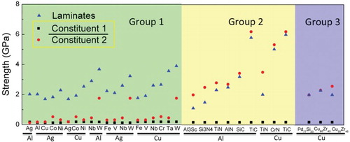
Figure 4. Stress fields in 10 nm Al—5 nm TiN in association with the deposited interface dislocations with the average spacing of 10 nm, showing (a) the normal stress parallel to the interface and (b) the resolved shear stress with respect to a glide plane (denoted as dashed white lines) [Citation83].
![Figure 4. Stress fields in 10 nm Al—5 nm TiN in association with the deposited interface dislocations with the average spacing of 10 nm, showing (a) the normal stress parallel to the interface and (b) the resolved shear stress with respect to a glide plane (denoted as dashed white lines) [Citation83].](/cms/asset/9867a3c5-fd6e-4538-93c2-28c90913e2d5/tmrl_a_1225321_f0004_c.jpg)
Figure 5. Schematic of key strengthening mechanisms in nanolaminates: (a) coherency stresses associated with lattice-matched nanolayers, (b) discontinuity of slip across twin interface, (c) glide dislocations pinned by grid of misfit dislocations at a semi-coherent interface, and (d) cross-slip of lattice dislocation in the weak shear interface.
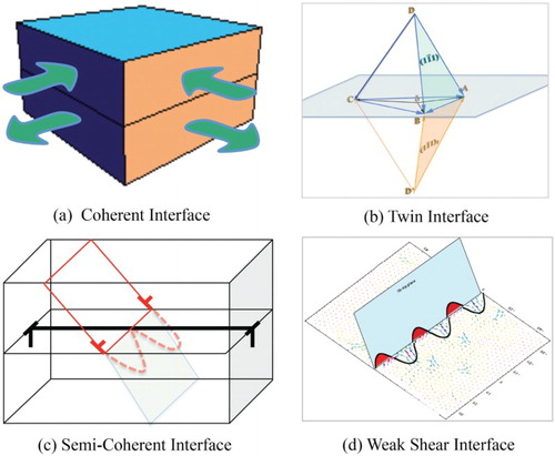
Figure 6. The maximum resolved shear stress required to accomplish the slip transmission as a function of interface shear strength [Citation111].
![Figure 6. The maximum resolved shear stress required to accomplish the slip transmission as a function of interface shear strength [Citation111].](/cms/asset/5fcbe5e2-7dec-45a4-98c0-4a4dd7b552c4/tmrl_a_1225321_f0006_c.jpg)
Figure 7. (a) Molecular dynamics simulations demonstrated dislocation climb along the Cu–Nb interface [Citation123], and (b1–b3) in situ TEM observations of dislocation climb along the Al–Nb interface [Citation115]. Climb of the out-of-plane component of interfacial dislocations is ascribed to (c) a high equilibrium vacancy concentration of 5.8% at 300 K and a low kinetic barrier of 0.03–0.10 eV for vacancy migration in the interface [Citation55,Citation128].
![Figure 7. (a) Molecular dynamics simulations demonstrated dislocation climb along the Cu–Nb interface [Citation123], and (b1–b3) in situ TEM observations of dislocation climb along the Al–Nb interface [Citation115]. Climb of the out-of-plane component of interfacial dislocations is ascribed to (c) a high equilibrium vacancy concentration of 5.8% at 300 K and a low kinetic barrier of 0.03–0.10 eV for vacancy migration in the interface [Citation55,Citation128].](/cms/asset/25a2f17a-417a-4363-b4ef-fe69d5b52d9a/tmrl_a_1225321_f0007_c.jpg)
Figure 8. (a) Measured true stress—strain curve of nanotwinned Cu foils. (b) Cross-sectional TEM micrographs of nanotwinned Cu films after 50% thickness reduction, showing a high density of dislocations along twin boundaries without dislocation cell walls in layers [Citation103]. (c) The crystallography of slips in nanotwinned multilayers shows three paired {111} slip systems across the twin interface. (d) Lomer dislocations at the twin interface as a reaction result of the deposited interface dislocations. (e) The crystallography of slips in the KS fcc–bcc system shows three paired {111} slip systems across the interface. (f) A small residual dislocation results from the reaction of the deposited interface dislocations.
![Figure 8. (a) Measured true stress—strain curve of nanotwinned Cu foils. (b) Cross-sectional TEM micrographs of nanotwinned Cu films after 50% thickness reduction, showing a high density of dislocations along twin boundaries without dislocation cell walls in layers [Citation103]. (c) The crystallography of slips in nanotwinned multilayers shows three paired {111} slip systems across the twin interface. (d) Lomer dislocations at the twin interface as a reaction result of the deposited interface dislocations. (e) The crystallography of slips in the KS fcc–bcc system shows three paired {111} slip systems across the interface. (f) A small residual dislocation results from the reaction of the deposited interface dislocations.](/cms/asset/7c7a6f7c-c892-4023-aa5a-87ad5ead3180/tmrl_a_1225321_f0008_c.jpg)
Figure 9. (a) High-resolution transmission electron microscope (HRTEM) image of a typical cube-on-cube Cu–Ag interface and (b) fine twin bands in the cube-on-cube Cu–Ag composite. (c) HRTEM image of a typical hetero-twin Cu–Ag interface and (d) a shear band in the hetero-twin Cu–Ag composite. Three paired slip systems form the threefold crystallographic symmetry of slip systems about the normal of the interface [Citation65].
![Figure 9. (a) High-resolution transmission electron microscope (HRTEM) image of a typical cube-on-cube Cu–Ag interface and (b) fine twin bands in the cube-on-cube Cu–Ag composite. (c) HRTEM image of a typical hetero-twin Cu–Ag interface and (d) a shear band in the hetero-twin Cu–Ag composite. Three paired slip systems form the threefold crystallographic symmetry of slip systems about the normal of the interface [Citation65].](/cms/asset/fe20936b-be46-4ef3-a6e0-c7cc80a96970/tmrl_a_1225321_f0009_c.jpg)
Figure 10. (a) HRTEM image of a typical KS Cu{111}–Nb{110} interface and (b) a shear band in the composite [Citation65]. (c) HRTEM image of a typical KS Cu{112}–Nb{112} interface and (d) a shear band in the composite. The white lines in (a) and green lines in (c) indicate the favorably paired slip systems. (e) and (f) TEM images of (d), showing fine twins and stacking faults in the Cu layer that are parallel to the favorably paired slip plane.
![Figure 10. (a) HRTEM image of a typical KS Cu{111}–Nb{110} interface and (b) a shear band in the composite [Citation65]. (c) HRTEM image of a typical KS Cu{112}–Nb{112} interface and (d) a shear band in the composite. The white lines in (a) and green lines in (c) indicate the favorably paired slip systems. (e) and (f) TEM images of (d), showing fine twins and stacking faults in the Cu layer that are parallel to the favorably paired slip plane.](/cms/asset/46e60377-4f35-417f-aa9b-f197f8119fd4/tmrl_a_1225321_f0010_c.jpg)
Figure 11. TEM images of the 40 nm CuZr/Cu multilayer after indentation testing. (a) Six shear bands outlined in the yellow rectangles and (b) the shear bands SB1 and SB2 end at the CuZr–Cu interfaces. (c) and (d) slip bands in the Cu layers that formed associated with shear on {111} planes nonparallel to the layers. The thin red line in (c) and (d) represents {111} planes in the Cu. Two tilt grain boundaries, GB1 and GB2, are marked in (c), indicating that shear also occurs on the {111} plane parallel to the layers. The regions outlined by the yellow circles show a crystalline structure in the CuZr.
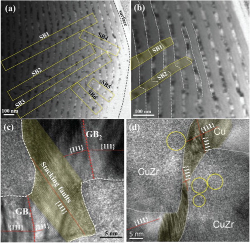
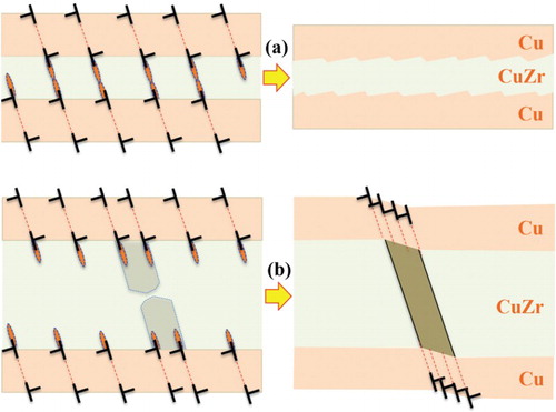
Figure 12. Schematics of plastic deformation modes with respect to the CuZr layer thickness. (a) Plastic co-deformation in the thin CuZr layers, showing plastic deformation in the Cu layers via slip on {111} planes and the formation and reaction of STZs in the CuZr layers. The red ellipses represent STZs. (b) The formation and propagation of shear bands in the thick CuZr layers, showing propagation of shear bands into the Cu layers, are accomplished via the formation of slip bands on {111} planes. The dashed lines represent {111} planes nonparallel to the layers.