Figures & data
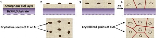
Figure 1. (a) Schematic of the synthesis process. (b) TEM bright-field image showing crystalline Ti seeds on an amorphous TiAl layer. (c) HR-TEM image showing the atoms on the (0001) plane of a Ti seed (red circle) surrounded by the amorphous TiAl matrix. The CBED pattern of the seed is shown in the inset. (d) TEM bright-field image of an as-deposited 40 nm amorphous TiAl film with a 1 nm Ti seed layer in the middle. EDS analysis of the seed region (right, red arrow) and the amorphous matrix (left, blue arrow) reveals the difference in their composition. Note that the composition of the seed region includes the amorphous matrix encapsulating the seed.
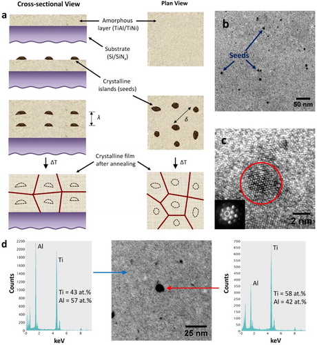
Figure 2. TEM bright-field image of a TiAl film with no seed layer after 2 h of annealing at 550°C. This film remained completely amorphous as indicated by the diffuse ring in the selected area diffraction (SAD) pattern (inset). (b) TEM bright-field image of a TiAl film with a single 1 nm Ti seed layer in the middle after 2 h of annealing at 550°C. The film showed partial crystallization and spots started to appear in the SAD pattern (inset). (c) XRD pattern of the film in (b). The presence of a well-defined gamma-TiAl (111) peak indicates that the film has started to crystallize.
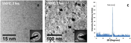
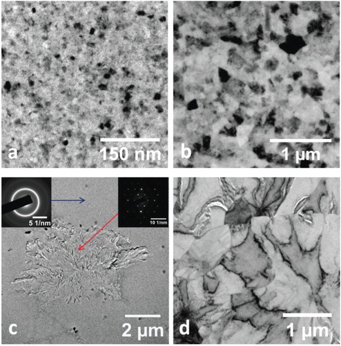
Figure 3. Post-annealing bright-field TEM images of: (a) TiAl film with no seed layer (dm = 1.15 ± 0.2 µm). (b) TiAl film with a single 1 nm Ti seed layer (dm = 65 ± 35 nm). (c) TiAl film with a single 1 nm Ti seed layer (dm = 67 ± 39 nm). (d) TiNi film with no seed layer (dm = 1.44 ± 0.29 µm). (e) TiNi film with a single 1 nm Ti seed layer (dm = 540 ± 150 nm). (f) TiNi film with a single 1 nm Ti (dm = 580 ± 124 nm). All the films were 100 nm thick and the annealing temperature and time are indicated in the images. For all seeded films, the seed layer was deposited in the middle. The ± values in dm correspond to the standard deviation.
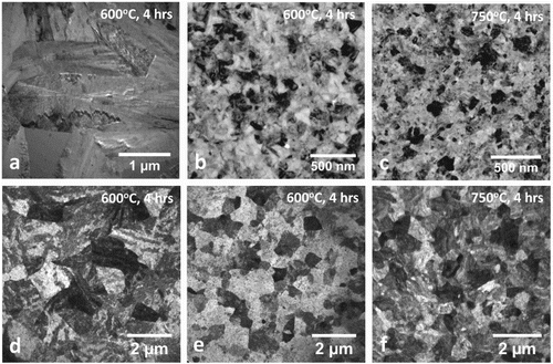
Figure 4. TEM bright-field images of three different 100 nm thick TiAl films with a single 1 nm Ti seed layer (deposited in the middle) after annealing at 600°C for 4 h. In addition to the final 600°C annealing, the films in (b) and (c) were subjected to a 10 min anneal at 100°C and 150°C, respectively, immediately after seed layer deposition. The mean grain sizes are 65 ± 35 nm, 141 ± 50 nm and 176 ± 65 nm for the films in (a), (b) and (c), respectively.
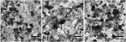
Figure 5. Cross-sectional TEM bright-field images of: (a) TiAl film with a single 1 nm Ti seed layer in the middle. (b) TiAl film with four equally spaced 1 nm Ti seed layers. (c) TiAl film with smaller seed layer spacing near the top and bottom and larger spacing in the middle. A gradient microstructure was formed upon annealing. (d) TiNi film with a single 1 nm Ti seed layer in the middle. (e) TiNi film with four equally spaced 1 nm Ti seed layers. (f) TiNi film with multiple seed layers and varying λ. A gradient microstructure was formed after annealing, similar to (c). All the films were annealed at 650°C for 4 h. The red arrows indicate the TiAl and TiNi film cross-sections.
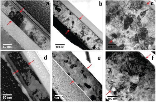
Figure 6. (a–b) TEM images from in-situ annealing of a 100 nm thick TiAl film with a single 1 nm Ti seed layer. (a) shows the film after heating at 550°C for 1 h, whereas (b) corresponds to the film after heating at 650°C for a further 30 min. (c–d) TEM images from in-situ annealing of an unseeded 100 nm thick TiAl film. (c) corresponds to 600°C annealing for 1 h and shows the nucleation of a large crystalline phase (red arrow), as revealed by the SAD pattern. The rest of the film (blue arrow) was still amorphous. (d) corresponds to further annealing at 650°C for 30 min and shows the formation of µm-sized grains.