Figures & data
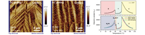
Figure 1. The piezoelectric and dielectric properties of ACP and DCP samples: (a) the piezoelectric coefficient of DCP and ACP with different number of cycles; the inset shows the poling electric field and duration time; (b) the free and clamped dielectric constant of DCP and ACP with different number of cycles; (c) the dielectric constant of five samples under unpoled, DCP and ACP conditions, where the error bar shows the deviation of three tests from each sample; (d) the dielectric constant of DCP and ACP samples at different poling electric fields.
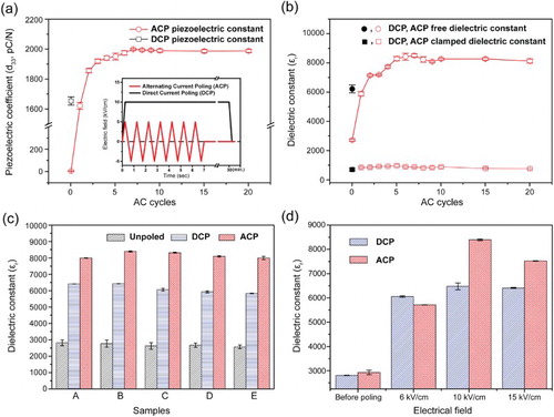
Figure 2. The XRD (400) reflection of PMN-PT single crystal resulting from different poling methods, including ACP, DCP and unpoled sample in the room temperature. The peak intensities have been normalized and the reference patterns are shown in the bottom of the figure.
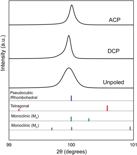
Figure 3. The PFM images of domain morphology for PMN-30%PT in different poling conditions: (a) unpoled (E = 0 kV/cm), (b) using DCP method, (c) using ACP method (1 Hz, 7 cycles). The poling field is 10 kV/cm and along [001] direction. The scanned plane is (010) cross section plane.
![Figure 3. The PFM images of domain morphology for PMN-30%PT in different poling conditions: (a) unpoled (E = 0 kV/cm), (b) using DCP method, (c) using ACP method (1 Hz, 7 cycles). The poling field is 10 kV/cm and along [001] direction. The scanned plane is (010) cross section plane.](/cms/asset/9b3147ae-e461-4e64-b716-f6de44c45e1c/tmrl_a_1498812_f0003_c.jpg)
Figure 4. Dielectric constant as function of temperature for PMN-PT single crystal after (a) DCP and (b) ACP processes (including 3 cycles, 7 cycles, and 20 cycles for the ACP process). (c) (004) peaks showing T and R phase coexistence during the phase transition near 90°C in ACP sample (7 cycles).
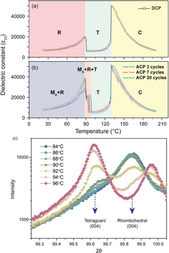
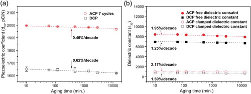
Figure 5. The aging rate of DCP and ACP. (a) The aging rate of piezoelectric coefficient, (b) The aging rate of free and clamped dielectric constant.