Figures & data
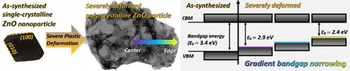
Figure 1. The change of ZnO particles morphology and microstructure caused by HPT processing. SEM images of as-synthesized (a) and compacted (b) ZnO particles with average particle sizes of 311 ± 150 nm and 304 ± 149 nm, respectively; (c) a BF-TEM image of as-synthesized ZnO particles; insert and arrows highlight the thickness fringes at the edge of the particles; (d) a SEM image of HPT-processed ZnO particles having average dimensions of 603 ± 243 nm and 78 ± 42 nm along the shearing direction (SD) and normal direction (ND), respectively; (e) a BF-TEM image of an HPT-processed ZnO particle; insert shows a SADP taken from the particle.
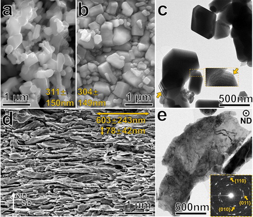
Figure 2. The wedge-like shape of the edge region on HPT-processed ZnO particles. (a) a schematic illustration of the frictional sliding, shear deformation and consolidation of the HPT-processed ZnO particles; (b) an ADF-STEM image of two HPT-processed ZnO particles with an overlap region, indicating that frictional sliding may occur between them; (c) a map of the relative thickness, t/λ, taken from a particle edge region highlighted in (b). The absolute thickness changes gradually from 0.32λ (29 nm) to 1.14λ (104 nm) from the edge to the interior of the particle, within a distance of 225 nm along the particle surface.
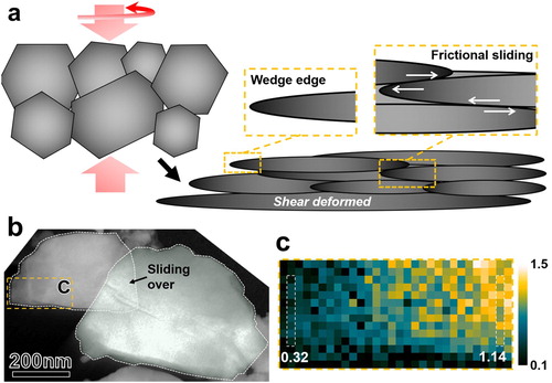
Figure 3. Gradient bandgap narrowing at the edge of an HPT-processed ZnO particle. (a) the ADF image of a deformed ZnO particle on which seven EELS acquisition locations are labeled; (b) a relative thickness map showing the t/λ changes from 0.22 at the outermost edge to 0.78 within 120 nm towards the interior of the particle; (c) seven VEEL spectra after ZLP and background subtraction. Note the increase of slopes of the low-loss spectra from point #1 to #7 with increasing thickness. Furthermore, the intensity of the humps before the bandgap onsets increased along with increasing thickness due to greater Cerenkov and surface effects.
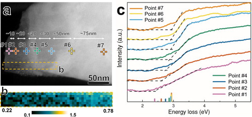
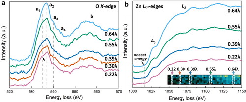
Figure 4. The evolution of valence band maximum and conduction band minimum at the edge region studied by core-loss EELS of (a) O K-edge and (b) Zn L2,3-edge. The spectra are averaged from the strips shown in the insert in (b), and the background signals were subtracted. Note the arrow in (a) pointing at the characteristic peak a1.