Figures & data
Figure 1. (a) Top, side and cross-sectional views of the nanoscratch track. (b, c) Post-nanoscratch SEM surface morphologies of micron-grain HEO and nano-grain HEO, respectively. (d, e) Depth profiles plotted for applied normal load values of 50 and 150 mN, respectively.
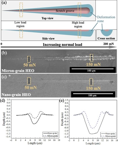
Figure 2. Cross section of the room temperature nanoscratch-tested micron-grain HEO at ∼150 mN applied normal load: (a) Bright-field STEM image displaying the deformation zone below the scratch groove. (b) Bright-field STEM image showing the representative microstructure farther away from the scratch groove and outside the deformation zone. (c) Higher magnification bright-field STEM image of the region in (a). (d) Dark-field STEM image from the region marked in (a) showing a high density of dislocations formed during nanoscratch testing.
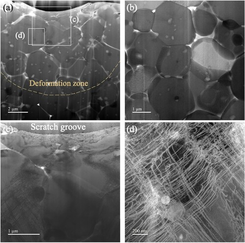
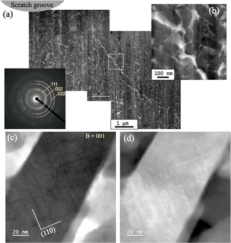
Figure 3. Dislocation analysis in room temperature nanoscratch-tested micron-grain HEO at ∼150 mN applied normal load: (a, b) Two beam bright-field and weak-beam dark-field TEM images with g = 1–11 near [011] zone axis. (c, d) Two beam bright-field and weak-beam dark-field TEM images of the same region as in (a, b) with g = −1–11 near the [011] zone axis. The dislocations observed are <110>{1–10} type. The star marks the same location in the sample to guide the eye.
![Figure 3. Dislocation analysis in room temperature nanoscratch-tested micron-grain HEO at ∼150 mN applied normal load: (a, b) Two beam bright-field and weak-beam dark-field TEM images with g = 1–11 near [011] zone axis. (c, d) Two beam bright-field and weak-beam dark-field TEM images of the same region as in (a, b) with g = −1–11 near the [011] zone axis. The dislocations observed are 12<110>{1–10} type. The star marks the same location in the sample to guide the eye.](/cms/asset/e383da91-ffa8-4b15-907d-96ec79112ff8/tmrl_a_2135409_f0003_ob.jpg)
Figure 4. Dislocation structures in room temperature nanoscratch-tested micron-grain HEO at ∼150 mN applied normal load: (a) STEM image along [001] showing dislocations appear as straight lines parallel to the traces of {110} planes. (b) High-resolution STEM image of the white square region in (a), showing dislocation cores of edge <110>{1–10} dislocations. (c) High-resolution STEM image of screw dislocations. (d) IFFT image of the region marked by a white square in (c) showing the core of a screw dislocation marked by a white line.
![Figure 4. Dislocation structures in room temperature nanoscratch-tested micron-grain HEO at ∼150 mN applied normal load: (a) STEM image along [001] showing dislocations appear as straight lines parallel to the traces of {110} planes. (b) High-resolution STEM image of the white square region in (a), showing dislocation cores of edge 12<110>{1–10} dislocations. (c) High-resolution STEM image of screw dislocations. (d) IFFT image of the region marked by a white square in (c) showing the core of a screw dislocation marked by a white line.](/cms/asset/a5e3fb56-2328-40c2-aad5-2c82fa8b6e82/tmrl_a_2135409_f0004_oc.jpg)
Figure 5. Cross-section of room temperature nanoscratch tested nano-grain HEO at ∼150 mN applied normal load: (a) A montage of bright-field TEM images of the deformation zone below the scratch groove. Inset is the selected area diffraction pattern showing diffraction rings for single-phase rocksalt structure. (b) Zoomed in bright-field TEM of the region in (a) showing intergranular path of the micro-crack. (c, d) STEM bright and annular dark-field images of a nano-scale grain in the deformation zone. The dislocations within the grain are mostly screw type <110>{1–10} dislocations.