Figures & data

Figure 1. Quantum confinement in 2D materials. Schematics showing (a) the exciton Bohr radius [Citation7] and (b) the diffusion length [Citation12, Citation13, Citation14], and (c) the mean free path of free electrons [Citation15, Citation21]. They are three factors to be considered for designing and engineering the quantum confinement effects in 2D materials.
![Figure 1. Quantum confinement in 2D materials. Schematics showing (a) the exciton Bohr radius [Citation7] and (b) the diffusion length [Citation12, Citation13, Citation14], and (c) the mean free path of free electrons [Citation15, Citation21]. They are three factors to be considered for designing and engineering the quantum confinement effects in 2D materials.](/cms/asset/92220da9-6521-4706-9182-e9ba62641eca/tmrl_a_2151852_f0001_oc.jpg)
Figure 2. Approaches for spatially controlled growth of 2D quantum heterostructures. (a) Schematic of ‘Sequential epitaxy’ process, in which a new 2D layer is formed either vertically or laterally onto the pre-deposited 2D material by sequentially supplying sources. (b) Schematic of ‘Etching and regrowth’ process, in which a part of a 2D material is etched and then filled with another material via a chemical reaction. (c) Schematic of ‘Conversion’ technique for converting a preformed crystal into another crystal by a source supply during the thermal CVD. (d) Schematic of ‘One-pot growth’ process, showing a growth method that simultaneous growth of 2D heterostructure with different precursors in the same reactor.
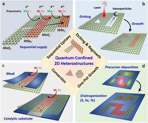
Table 1. Summary of the spatially controlled growth of 2D lateral and vertical heterostructures. Lateral and vertical heterostructures are denoted by A-B and A/B, respectively.
Figure 3. Sequential epitaxial growth of vertical/lateral 2D heterostructures. (a, b) Determination of lateral/vertical growth aspects by the W/Se ratio during the two-step CVD [Citation26]. (a) Schematic of controllable lateral edge-mediated growth and vertical vdW epitaxy of heterostructures composed of MoS2 and WSe2 depending on the adsorption of various active clusters of W1Sex. (b) The diffusion barriers of W1Se3 and W1Se1 clusters on the edge/basal surface of the MoS2 layer. (c-e) Edge-mediated epitaxy of lateral WS2-WSe2-WS2 heterostructure [Citation31]. (c) Schematic of the edge-mediated epitaxy of lateral heterostructures. (d) High-resolution scanning transmission electron microscopy (STEM) image of the WS2-WSe2 lateral heterostructure (left). Magnified STEM image of the dashed red rectangle region (top right) and the corresponding atomic model (bottom right). (e) Scanning electron microscopy (SEM) images of the lateral WS2-WSe2-WS2 multi-heterojunction with ultra-narrow WSe2 width (∼35 and 13 nm) with different growth times (10 and 5 s). (f) vdW epitaxy of vertical MoS2/WS2 heterostructures [Citation37]. Flow-rate modulations of the metal-organicprecursors for the growth of (top) and a series of cross-sectional high-angle annular dark field (HAADF)-STEM images of the heterostructures depending on the flow rate (bottom) are shown. (g-i) Capillary force-driven rolling-up strategy for the fabrication of vdW superlattice [Citation39]. (g) Schematic illustration of the fabrication process of roll-up vdW superlattices. (h) STEM image of a rolled-up SnS2/WSe2 heterostructure. (i) STEM image (left) and corresponding energy-dispersive spectroscopy (EDS) mapping images (center: W, right: Sn) of the SnS2/WSe2 vdW superlattice.
![Figure 3. Sequential epitaxial growth of vertical/lateral 2D heterostructures. (a, b) Determination of lateral/vertical growth aspects by the W/Se ratio during the two-step CVD [Citation26]. (a) Schematic of controllable lateral edge-mediated growth and vertical vdW epitaxy of heterostructures composed of MoS2 and WSe2 depending on the adsorption of various active clusters of W1Sex. (b) The diffusion barriers of W1Se3 and W1Se1 clusters on the edge/basal surface of the MoS2 layer. (c-e) Edge-mediated epitaxy of lateral WS2-WSe2-WS2 heterostructure [Citation31]. (c) Schematic of the edge-mediated epitaxy of lateral heterostructures. (d) High-resolution scanning transmission electron microscopy (STEM) image of the WS2-WSe2 lateral heterostructure (left). Magnified STEM image of the dashed red rectangle region (top right) and the corresponding atomic model (bottom right). (e) Scanning electron microscopy (SEM) images of the lateral WS2-WSe2-WS2 multi-heterojunction with ultra-narrow WSe2 width (∼35 and 13 nm) with different growth times (10 and 5 s). (f) vdW epitaxy of vertical MoS2/WS2 heterostructures [Citation37]. Flow-rate modulations of the metal-organicprecursors for the growth of (top) and a series of cross-sectional high-angle annular dark field (HAADF)-STEM images of the heterostructures depending on the flow rate (bottom) are shown. (g-i) Capillary force-driven rolling-up strategy for the fabrication of vdW superlattice [Citation39]. (g) Schematic illustration of the fabrication process of roll-up vdW superlattices. (h) STEM image of a rolled-up SnS2/WSe2 heterostructure. (i) STEM image (left) and corresponding energy-dispersive spectroscopy (EDS) mapping images (center: W, right: Sn) of the SnS2/WSe2 vdW superlattice.](/cms/asset/ee564ece-0f4a-4e6b-a870-9a3d93789039/tmrl_a_2151852_f0003_oc.jpg)
Figure 4. Etching and regrowth process for the production of vertical/lateral 2D heterostructures. (a, b) Synthesis of periodic monolayer 2D heterostructures by laser-pattering and thermal etching process [Citation41]. (a) Schematic illustration of the growth process consists of laser patterning and thermal etching of the pre-deposited WS2 matrix followed by the growth of WSe2. (b) Optical microscopy (OM) image of a lateral heterostructure with WSe2 crystals embedded in a monolayer WS2 matrix. (c, d) Synthesis of chirality-controlled graphene nanoribbons (GNR) embedded in hBN [Citation44]. (c) Schematic showing the strategy to prepare GNRs with crystallographic edge orientations. Different particles of Ni or Pt etch nano-trenches with different edge topologies (Ni: zigzag, Pt: armchair) in an hBN layer. (d) AFM image of 1D GNR with zigzag terminations embedded in 2D hBN. (e, f) Vertical growth of VSe2 on WSe2 by incomplete etching of the WSe2 [Citation45]. (e) Schematic of the vertical growth process by laser irradiation. (f) OM image of periodic arrangements of VSe2/WSe2 heterostructure arrays.
![Figure 4. Etching and regrowth process for the production of vertical/lateral 2D heterostructures. (a, b) Synthesis of periodic monolayer 2D heterostructures by laser-pattering and thermal etching process [Citation41]. (a) Schematic illustration of the growth process consists of laser patterning and thermal etching of the pre-deposited WS2 matrix followed by the growth of WSe2. (b) Optical microscopy (OM) image of a lateral heterostructure with WSe2 crystals embedded in a monolayer WS2 matrix. (c, d) Synthesis of chirality-controlled graphene nanoribbons (GNR) embedded in hBN [Citation44]. (c) Schematic showing the strategy to prepare GNRs with crystallographic edge orientations. Different particles of Ni or Pt etch nano-trenches with different edge topologies (Ni: zigzag, Pt: armchair) in an hBN layer. (d) AFM image of 1D GNR with zigzag terminations embedded in 2D hBN. (e, f) Vertical growth of VSe2 on WSe2 by incomplete etching of the WSe2 [Citation45]. (e) Schematic of the vertical growth process by laser irradiation. (f) OM image of periodic arrangements of VSe2/WSe2 heterostructure arrays.](/cms/asset/7f8ca24b-ce71-4634-9686-f8678f1496fa/tmrl_a_2151852_f0004_oc.jpg)
Figure 5. Post-synthetic conversion process to achieve lateral 2D heterostructures. (a, b) Position-controlled conversion of 2D materials for the growth of lateral MoS2-MoS2 heterostructures [Citation49]. (a) Patterning and selective conversion of 2D materials using SiO2 masking layers for MoSe2-MoS2 heterostructures. (b) Raman mappings of MoS2-MoSe2 lateral heterojunction arrays formed within monolayer crystals by patterning and selective conversion processes. (c-e) Spatially controlled conversion process from hBN to graphene [Citation52, Citation53]. (c) Schematic illustrations for the conversion process of hBN on Pt substrate to produce 2D lateral heterostructure of graphene-hBN [Citation52]. (d, e) Schematic (d) and SEM image (e) of graphene quantum dots embedded in the hBN matrix, grown by the selective conversion on an array of the Pt nanoparticles. [Citation53]. (f) Schematic of the patterning process guided by misfit dislocations (marked as ‘T’) at the MoS2-WSe2 lateral heterojunction. (g) STEM images of MoS2 1D channels embedded within WSe2. (h) STEM image (left) and strain map (right) of a MoS2 1D channel formed from an intrinsic 5|7 dislocation in WSe2 [Citation55].
![Figure 5. Post-synthetic conversion process to achieve lateral 2D heterostructures. (a, b) Position-controlled conversion of 2D materials for the growth of lateral MoS2-MoS2 heterostructures [Citation49]. (a) Patterning and selective conversion of 2D materials using SiO2 masking layers for MoSe2-MoS2 heterostructures. (b) Raman mappings of MoS2-MoSe2 lateral heterojunction arrays formed within monolayer crystals by patterning and selective conversion processes. (c-e) Spatially controlled conversion process from hBN to graphene [Citation52, Citation53]. (c) Schematic illustrations for the conversion process of hBN on Pt substrate to produce 2D lateral heterostructure of graphene-hBN [Citation52]. (d, e) Schematic (d) and SEM image (e) of graphene quantum dots embedded in the hBN matrix, grown by the selective conversion on an array of the Pt nanoparticles. [Citation53]. (f) Schematic of the patterning process guided by misfit dislocations (marked as ‘T’) at the MoS2-WSe2 lateral heterojunction. (g) STEM images of MoS2 1D channels embedded within WSe2. (h) STEM image (left) and strain map (right) of a MoS2 1D channel formed from an intrinsic 5|7 dislocation in WSe2 [Citation55].](/cms/asset/91566b71-8b74-41f0-8711-9b8ef4a1d7e0/tmrl_a_2151852_f0005_oc.jpg)
Figure 6. Simultaneous, one-pot synthesis of vertical or lateral 2D heterostructures. (a, b) Simultaneous integration of metallic 1T’-MoTe2 and semiconducting 2H-MoTe2 by tellurization of patterned precursors of MoO3 and MoO3-x [Citation56]. (a) Schematic for the growth of lateral heterostructure of 1T’−2H MoTe2 heterojunction. (b) STEM image of the heterojunction (inset: SEM image). (c, d) Direct synthesis of vertical 2D Mo2C/graphene heterostructure using molten Mo-Cu alloy catalyst and high CH4 concentration during the CVD [Citation59]. (c) Schematic of the growth process, and (d) OM image of Mo2C crystals on a graphene monolayer.
![Figure 6. Simultaneous, one-pot synthesis of vertical or lateral 2D heterostructures. (a, b) Simultaneous integration of metallic 1T’-MoTe2 and semiconducting 2H-MoTe2 by tellurization of patterned precursors of MoO3 and MoO3-x [Citation56]. (a) Schematic for the growth of lateral heterostructure of 1T’−2H MoTe2 heterojunction. (b) STEM image of the heterojunction (inset: SEM image). (c, d) Direct synthesis of vertical 2D Mo2C/graphene heterostructure using molten Mo-Cu alloy catalyst and high CH4 concentration during the CVD [Citation59]. (c) Schematic of the growth process, and (d) OM image of Mo2C crystals on a graphene monolayer.](/cms/asset/0dbe6dbe-40bf-4716-9d2e-66a1ce8a0afc/tmrl_a_2151852_f0006_oc.jpg)
Figure 7. Promising applications of vertical or lateral 2D heterostructures. (a, b) Light-emitting diode (LED) based on vertical heterostructures composed of hBN, graphene, and TMD layers [Citation70]. (a) Schematic of band alignments, and (b) OM image showing the red-light emission from the LED of vdW heterostructure. (c, d) Self-powered photodetector fabricated using p-n Bi2Te3-WSe2 heterostructure [Citation38]. (c) OM image of the photodetector, and (d) photoresponse of the corresponding junction device with different light wavelengths (375, 520, 980, and 1550 nm). (e, f) Tunneling transistor application realized by using graphene quantum dots (GQD) embedded in hBN layers [Citation53]. (e) Modeling of the single-electron charging effect. (f) Conductance (G) as a function of Vg and Vb for a device with 10 nm-sized graphene quantum dots (QDs) measured at T = 0.25 K. (g, h) Quantum-confined electronic states in MoS2/WSe2 heterobilayers [Citation82]. (g) STM image and (h) conductance map taken along the yellow line in (g) for voltages in the valence band-edge region. (i, j) Lateral metal-semiconductor junction (MSJ) comprised of MoS2 and PtTe2 synthesized by two-step growth [Citation36]. (i) Schematic (top) and OM image (bottom) of the heterostructure. (j) Output electrical characteristics of MSJ transistor where the carriers are injected from PtTe2 (red) and Ti (blue). (k) The proposed quantum-confined heterostructure based on 0D QDs and 2D matrix with type-I band alignment, (left) the atomic schematic, and (right) the band structure.
![Figure 7. Promising applications of vertical or lateral 2D heterostructures. (a, b) Light-emitting diode (LED) based on vertical heterostructures composed of hBN, graphene, and TMD layers [Citation70]. (a) Schematic of band alignments, and (b) OM image showing the red-light emission from the LED of vdW heterostructure. (c, d) Self-powered photodetector fabricated using p-n Bi2Te3-WSe2 heterostructure [Citation38]. (c) OM image of the photodetector, and (d) photoresponse of the corresponding junction device with different light wavelengths (375, 520, 980, and 1550 nm). (e, f) Tunneling transistor application realized by using graphene quantum dots (GQD) embedded in hBN layers [Citation53]. (e) Modeling of the single-electron charging effect. (f) Conductance (G) as a function of Vg and Vb for a device with 10 nm-sized graphene quantum dots (QDs) measured at T = 0.25 K. (g, h) Quantum-confined electronic states in MoS2/WSe2 heterobilayers [Citation82]. (g) STM image and (h) conductance map taken along the yellow line in (g) for voltages in the valence band-edge region. (i, j) Lateral metal-semiconductor junction (MSJ) comprised of MoS2 and PtTe2 synthesized by two-step growth [Citation36]. (i) Schematic (top) and OM image (bottom) of the heterostructure. (j) Output electrical characteristics of MSJ transistor where the carriers are injected from PtTe2 (red) and Ti (blue). (k) The proposed quantum-confined heterostructure based on 0D QDs and 2D matrix with type-I band alignment, (left) the atomic schematic, and (right) the band structure.](/cms/asset/598ff10d-9f52-4e23-a088-489b916b42d2/tmrl_a_2151852_f0007_oc.jpg)
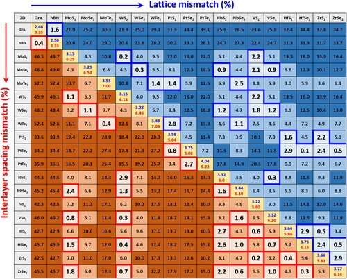
Figure 8. Lattice and interlayer spacing mismatch between TMDs. The values in yellow boxes on the central diagonal represent the lattice constant (top, blue) and interlayer spacing (bottom, red) of the TMDs, respectively. The values in the lower right (blue) and upper left boxes (red) are the lattice and spacing mismatch between each TMD, of which values less than 3% are highlighted. The lattice mismatch was calculated by simply considering the in-plane lattice distances of each unit cell of two materials.