Figures & data
Figure 1. X-ray diffraction patterns of the mixed (1-x)BNT-xBMT calcined powders with 2θ = 20–80°.
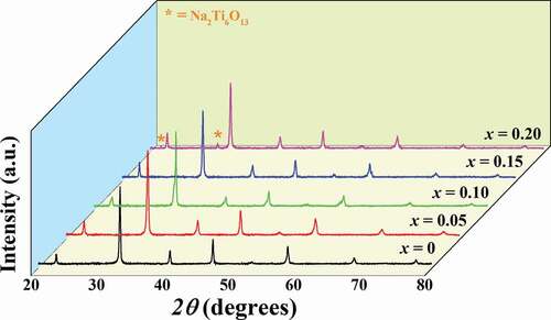
Table 1. Physical property, Microstructure, and XRD parameters of the (1-x)BNT-xBMT ceramics analysis by SmartLab Studio II
Figure 2. Plots of density value as a function of sintering temperature (1100–1200°C) of the (1-x)BNT-xBMT ceramics.
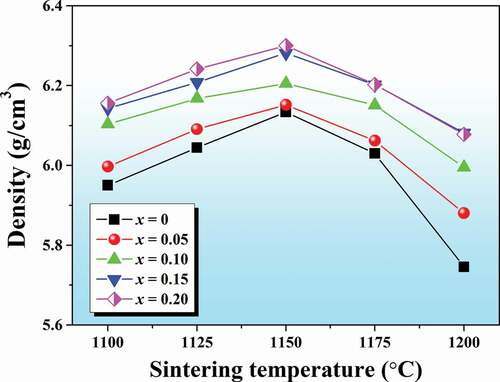
Figure 3. X-ray diffraction patterns of the (1-x)BNT-xBMT ceramics with 2θ = 20–80°.
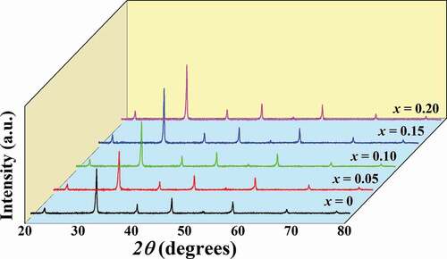
Figure 4. X-ray diffraction patterns of the (1-x)BNT-xBMT ceramics where x = 0–0.20 with 2θ = 20–80°, 39–41°, and 2θ = 45–48°.
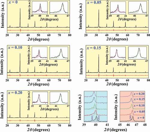
Figure 5. Plots of (a) unit cell volume and tolerance factor (t) values as a function of the BMT content, and (b) the rA and rB as a function of the BMT content of the (1-x)BNT-xBMT ceramics.
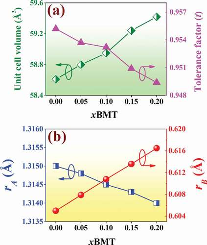
Figure 6. Raman spectra of the (1-x)BNT-xBMT ceramics measured at room temperature (RT) in the wavenumber range of 100–1400 cm−1.
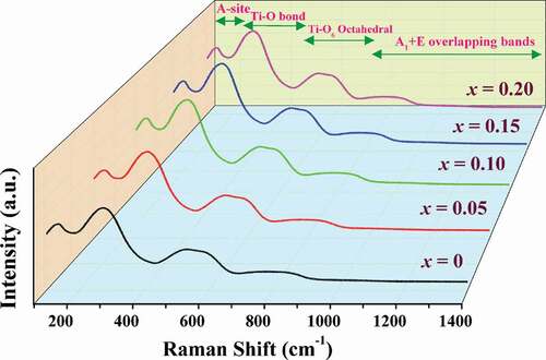
Table 2. Microstructure, dielectric, ferroelectric, and electric field-induced strain properties of the (1-x)BNT-xBMT ceramics
Figure 7. SEM micrographs with as sintered surfaces of the (1-x)BNT-xBMT ceramics where (a) x = 0, (b) x = 0.05, (c) x = 0.10, (d) x = 0.15, (e) x = 0.20, and (f) grain size as a function of BMT content.
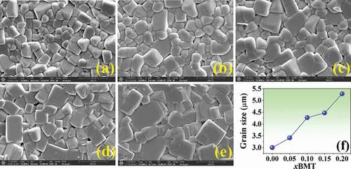
Figure 8. Temperature dependence of the dielectric constant (εr) and dielectric loss (tan δ) of the (1-x)BNT-xBMT ceramics measured at various frequencies from 1–500 kHz where (a) x = 0, (b) x = 0.05, (c) x = 0.10, (d) x = 0.15 (e) x = 0.20, and (f) plot of Tm and εmax values as a function of BMT content (inset: δA as a function of the BMT content).
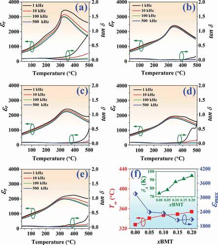
Figure 9. Polarization-electric field (P-E) hysteresis loop and current-electric field (I-E) data of the (1-x)BNT-xBMT ceramics, measured at 50 kV/cm and a frequency of 1 Hz where (a) x = 0, (b) x = 0.05, (c) x = 0.10,(d) x = 0.15, (e) x = 0.20, and (f) plot of Pr and Ec values as a function of BMT content.
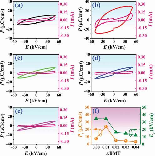
Figure 10. Temperature dependence on polarization-electric field (P-E) hysteresis loops of the (1-x)BNT-xBMT ceramics where x = 0–0.20, measured under an electric field of 50 kV/cm and a frequency of 1 Hz.
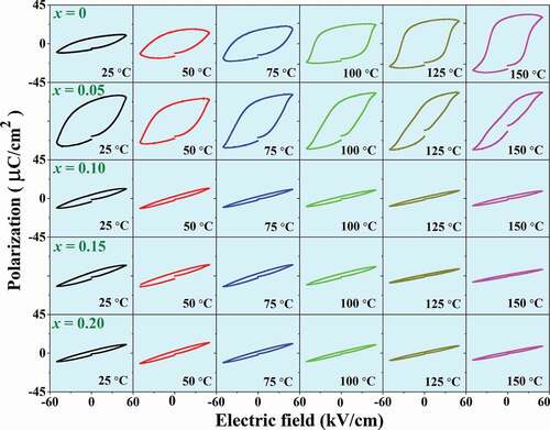
Table 3. Energy storage density, piezoelectric, and energy harvesting properties of the (1-x)BNT-xBMT ceramics
Figure 11. Plots of (a) Wrec as a function of temperature @ E = 50 kV, (b) η as a function of temperature @ E = 50 kV, (c) Wrec @ 125°C as a function of the electric field (until breakdown strength reached), and (d) Wrec @ 125°C as a function of BMT content and measured under E = 50 kV and E= Emax of the (1-x)BNT-xBMT ceramics.
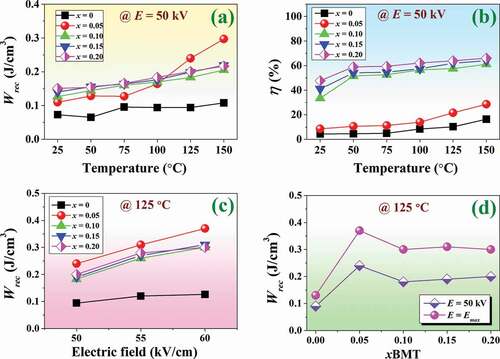
Figure 12. Bipolar strain-electric field (S-E) data of the (1-x)BNT-xBMT ceramics, measured under electric field of 70 kV/cm and a frequency of 0.1 Hz where (a) x = 0, (b) x = 0.05, (c) x = 0.10,(d) x = 0.15, (e) x = 0.20, and (f) plot of Smax and d*33 values as a function of BMT content.
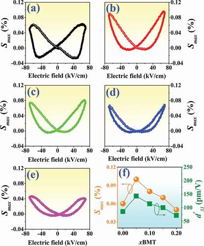
Figure 13. Plots of low-field d33 and g33 values as a function of BMT content of the (1-x)BNT-xBMT ceramics (the inset shows: FoM as a function of BMT content).
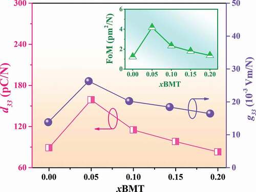
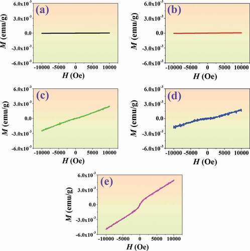
Figure 14. Plots of magnetization (M) and magnetic field (H) of the (1-x)BNT-xBMT ceramics, measured at RT and under the magnetic field of −10 kOe ≤ H ≤ 10 kOe, where (a) x = 0, (b) x = 0.05, (c) x = 0.10,(d) x = 0.15, and (e) x = 0.20.