Figures & data
Figure 1. The synthesis of TiN0.3, sintering synthesis and performance testing flowchart.
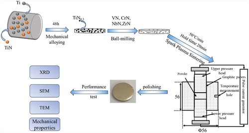
Figure 2. XRD data of five transition metal nitrides under Cu Kα radiation after SPS at different temperatures.
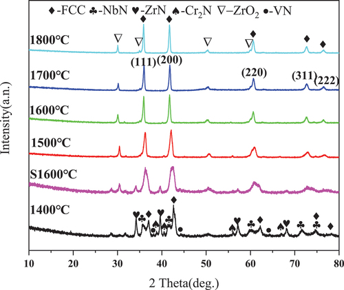
Table 1. Weight percentage of ZrO2 at different temperatures.
Figure 3. SEM schematic of SPS sintered samples at different temperatures: A: S1600°C, B: 1400°C, C: 1500°C, D: 1600°C, E: 1700°C, F: 1800°C.
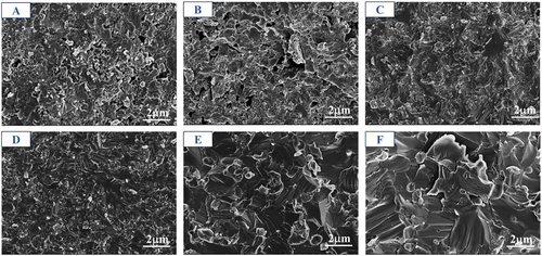
Figure 4. EDS energy spectrum of (TiVCrNbZr1-x)Ny-xZrO2 synthesized at 1700°C.
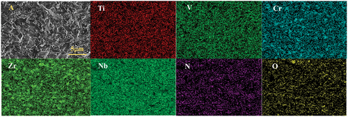
Figure 5. Point scanning of small particle point 1 in (A): (B) elemental content distribution map, (C) spectrograms.
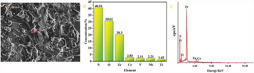
Table 2. Elemental content under EDS surface scanning at different sintering temperatures.
Figure 6. TEM analysis of the 1700°C samples: (A) BF-STEM image of the samples; (B) Spectral Array of Electron Diffraction (SAED) image under the [010] crystallographic band axis; (C) High Resolution Transmission Electron Microscopy (HRTEM) image; (D) and (E) IFFT images of the FCC phase and the ZrO2 phase, respectively.
![Figure 6. TEM analysis of the 1700°C samples: (A) BF-STEM image of the samples; (B) Spectral Array of Electron Diffraction (SAED) image under the [010] crystallographic band axis; (C) High Resolution Transmission Electron Microscopy (HRTEM) image; (D) and (E) IFFT images of the FCC phase and the ZrO2 phase, respectively.](/cms/asset/5f865d5d-e216-4609-bdbb-475fb3601ae0/tace_a_2360248_f0006_oc.jpg)
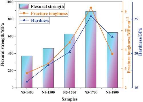
Figure 7. Schematic diagram of flexural strength, fracture toughness and hardness of samples at different temperatures.