
Figures & data
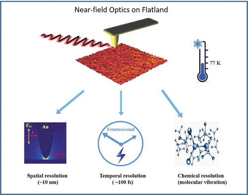
Figure 1. Schematic of near-field optics. (a) The comparison between far-field and near-field optics. The point spread function in far-field optics is determined by diffraction limit, while the spatial resolution in near-field optics is determined by the size of probe. (b) The explanation of breaking the diffraction limit in near-field optics based on uncertainty principle.
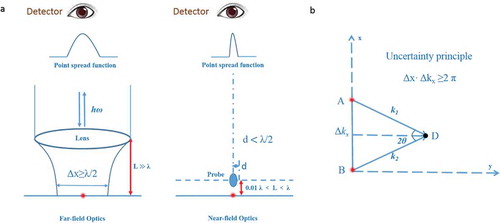
Figure 2. The comparison of four classical sub-wavelength approaches, including photon emission electron microscopy (PEEM), cathode-luminescence spectroscopy (CL), electron energy loss spectroscopy (EELS) and scanning near-field optical microscopy (SNOM).
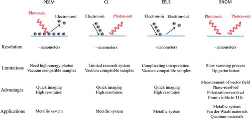
Figure 3. Experimental scheme of SNOM. (a) The illumination scheme of a-SNOM. (b) The illumination scheme of s-SNOM. (c) The scheme of oblique incidence-mode s-SNOM [Citation47]. (d) The scheme of transmission mode s-SNOM [Citation48]. (c) Reproduced with permission [Citation47]. Copyright 2002, Wiley-VCH. (d) Reproduced with permission [Citation48]. Copyright 2010, American Chemical Society.
![Figure 3. Experimental scheme of SNOM. (a) The illumination scheme of a-SNOM. (b) The illumination scheme of s-SNOM. (c) The scheme of oblique incidence-mode s-SNOM [Citation47]. (d) The scheme of transmission mode s-SNOM [Citation48]. (c) Reproduced with permission [Citation47]. Copyright 2002, Wiley-VCH. (d) Reproduced with permission [Citation48]. Copyright 2010, American Chemical Society.](/cms/asset/9074795f-3122-4946-acdd-bac1118f8715/tapx_a_1593051_f0003_oc.jpg)
Figure 4. The influence of AFM tip in near-field measurement. (a) Topography and near-field amplitude of a gold nanodisk obtained by carbon nanotube (CNT) tip and Pt-coated Si tip [Citation54]. Scale bar, 100 nm. (b) The numerical simulation of local electric field between AFM tip and substrate. (a) Reproduced with permission [Citation54]. Copyright 2009, American Physical Society.
![Figure 4. The influence of AFM tip in near-field measurement. (a) Topography and near-field amplitude of a gold nanodisk obtained by carbon nanotube (CNT) tip and Pt-coated Si tip [Citation54]. Scale bar, 100 nm. (b) The numerical simulation of local electric field between AFM tip and substrate. (a) Reproduced with permission [Citation54]. Copyright 2009, American Physical Society.](/cms/asset/5200690d-88df-4528-aef1-97d12748a65f/tapx_a_1593051_f0004_oc.jpg)
Figure 5. Near-field distribution around single metallic antennas in mid-infrared and visible range. (a) Near-field amplitude and phase of linear gold antenna with the incident wavelength at 11.06 μm [Citation57]. Scale bar, 1 μm. (b) Near-field amplitude and phase of gold nanorod structure with the incident wavelength at 632.8 nm [Citation65]. Scale bar, 100 nm. (c) Spectral shift between near- and far-field peak intensity of infrared gold antenna [Citation66]. (d) Near-field amplitude of gold triangle nanostructure with incident wavelength at 9.6 μm [Citation48]. Scale bar, 1 μm. (e) Near-field amplitude of silver nanoprisms with incident wavelength at 633 nm [Citation55]. Scale bar, 100 nm. (f) Near-field amplitude of gold nanodisks with incident wavelength at 875 nm [Citation56]. Scale bar, 200 nm. (g) Near-field amplitude of magnetic nickel nanodisks with incident wavelength at 633 nm [Citation67]. Scale bar, 100 nm. (a) Reproduced with permission [Citation57]. Copyright 2015, Wiley-VCH. (b) Reproduced with permission [Citation65]. Copyright 2014, American Chemical Society. (c) Reproduced with permission [Citation66]. Copyright 2013, American Physical Society. (d) Reproduced with permission [Citation48]. Copyright 2010, American Chemical Society. (e) Reproduced with permission [Citation55]. Copyright 2008, American Chemical Society. (f) Reproduced with permission [Citation56]. Copyright 2008, American Chemical Society. (g) Reproduced with permission [Citation67]. Copyright 2011, American Chemical Society.
![Figure 5. Near-field distribution around single metallic antennas in mid-infrared and visible range. (a) Near-field amplitude and phase of linear gold antenna with the incident wavelength at 11.06 μm [Citation57]. Scale bar, 1 μm. (b) Near-field amplitude and phase of gold nanorod structure with the incident wavelength at 632.8 nm [Citation65]. Scale bar, 100 nm. (c) Spectral shift between near- and far-field peak intensity of infrared gold antenna [Citation66]. (d) Near-field amplitude of gold triangle nanostructure with incident wavelength at 9.6 μm [Citation48]. Scale bar, 1 μm. (e) Near-field amplitude of silver nanoprisms with incident wavelength at 633 nm [Citation55]. Scale bar, 100 nm. (f) Near-field amplitude of gold nanodisks with incident wavelength at 875 nm [Citation56]. Scale bar, 200 nm. (g) Near-field amplitude of magnetic nickel nanodisks with incident wavelength at 633 nm [Citation67]. Scale bar, 100 nm. (a) Reproduced with permission [Citation57]. Copyright 2015, Wiley-VCH. (b) Reproduced with permission [Citation65]. Copyright 2014, American Chemical Society. (c) Reproduced with permission [Citation66]. Copyright 2013, American Physical Society. (d) Reproduced with permission [Citation48]. Copyright 2010, American Chemical Society. (e) Reproduced with permission [Citation55]. Copyright 2008, American Chemical Society. (f) Reproduced with permission [Citation56]. Copyright 2008, American Chemical Society. (g) Reproduced with permission [Citation67]. Copyright 2011, American Chemical Society.](/cms/asset/d66aa8c0-e1d3-4e65-99ab-fd61db9ef50a/tapx_a_1593051_f0005_oc.jpg)
Figure 6. Near-field distribution in nanogapped metallic antennas. (a) Near-field amplitude and phase of resonant gapped gold-antenna with incident wavelength at 11.1 μm [Citation69]. Scale bar, 2 μm. (b) Electromagnetic hotspots in gold-dimer nanostructures and corresponding enhanced Raman spectrum [Citation70]. The incident wavelength is 633 nm. Scale bar, 200 nm. (c) Near-field image of infrared nanofocusing in tapered transmission lines [Citation71]. The incident wavelength is 9.3 μm. (d) Near-field amplitude and phase distribution around nanoscale gap in inverse bowtie gold antenna [Citation24]. (a) Reproduced with permission [Citation69]. Copyright 2012, Nature Publishing Group. (b) Reproduced with permission [Citation70]. Copyright 2017, American Chemical Society. (c) Reproduced with permission [Citation71]. Copyright 2011, Nature Publishing Group. (d) Reproduced with permission [Citation24]. Copyright 2010, American Chemical Society.
![Figure 6. Near-field distribution in nanogapped metallic antennas. (a) Near-field amplitude and phase of resonant gapped gold-antenna with incident wavelength at 11.1 μm [Citation69]. Scale bar, 2 μm. (b) Electromagnetic hotspots in gold-dimer nanostructures and corresponding enhanced Raman spectrum [Citation70]. The incident wavelength is 633 nm. Scale bar, 200 nm. (c) Near-field image of infrared nanofocusing in tapered transmission lines [Citation71]. The incident wavelength is 9.3 μm. (d) Near-field amplitude and phase distribution around nanoscale gap in inverse bowtie gold antenna [Citation24]. (a) Reproduced with permission [Citation69]. Copyright 2012, Nature Publishing Group. (b) Reproduced with permission [Citation70]. Copyright 2017, American Chemical Society. (c) Reproduced with permission [Citation71]. Copyright 2011, Nature Publishing Group. (d) Reproduced with permission [Citation24]. Copyright 2010, American Chemical Society.](/cms/asset/55ec9d5b-c6ea-4f39-bdc7-d0f12b1ffe20/tapx_a_1593051_f0006_oc.jpg)
Figure 7. Near-field distribution of sophisticated metallic antennas. (a) Near-field images of progressively loaded nanoantennas [Citation72], including continuous rod, thick metal-bridge rod, tiny metal-bridge rod and fully cut rod. The length of gold rods is 1550 nm and the incident wavelength is 9.6 μm. (b) Near-field amplitude and phase of Fano interference in symmetric heptamer structures composed by seven gold nanodisks at a wavelength of 9.3 μm [Citation73]. (c) Near-field distribution around Archimedean spiral antennas illuminated by left (LCP) and right (RCP) circularly polarized light [Citation52]. The incident wavelength is 9.3 μm. (d) Near-field intensity and phase maps of V-shaped antennas for different sizes [Citation74]. The nano-infrared images demonstrate near-field phase varies as a function of antenna size. (a) Reproduced with permission [Citation72]. Copyright 2009, Nature Publishing Group. (b) Reproduced with permission [Citation73]. Copyright 2011, American Chemical Society. (c) Reproduced with permission [Citation52]. Copyright 2015, American Chemical Society. (d) Reproduced with permission [Citation74]. Copyright 2015, American Chemical Society.
![Figure 7. Near-field distribution of sophisticated metallic antennas. (a) Near-field images of progressively loaded nanoantennas [Citation72], including continuous rod, thick metal-bridge rod, tiny metal-bridge rod and fully cut rod. The length of gold rods is 1550 nm and the incident wavelength is 9.6 μm. (b) Near-field amplitude and phase of Fano interference in symmetric heptamer structures composed by seven gold nanodisks at a wavelength of 9.3 μm [Citation73]. (c) Near-field distribution around Archimedean spiral antennas illuminated by left (LCP) and right (RCP) circularly polarized light [Citation52]. The incident wavelength is 9.3 μm. (d) Near-field intensity and phase maps of V-shaped antennas for different sizes [Citation74]. The nano-infrared images demonstrate near-field phase varies as a function of antenna size. (a) Reproduced with permission [Citation72]. Copyright 2009, Nature Publishing Group. (b) Reproduced with permission [Citation73]. Copyright 2011, American Chemical Society. (c) Reproduced with permission [Citation52]. Copyright 2015, American Chemical Society. (d) Reproduced with permission [Citation74]. Copyright 2015, American Chemical Society.](/cms/asset/4cf3d896-0500-41c3-a317-cedb18f4bcfb/tapx_a_1593051_f0007_oc.jpg)
Figure 8. Polaritons in low-dimensional materials. Polaritons are collective excitation from coupling photons with other quasiparticles, such as plasmons in electron-rich systems, infrared-active phonons in polar insulators, excitons in semiconductors, cooper-pairs in superconductors, spin resonances in (anti)-ferromagnets and hybrids in heterostructures.
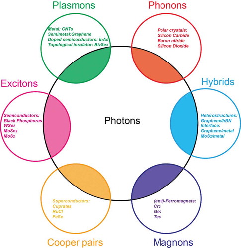
Figure 9. Surface plasmon polaritons in monolayer graphene. (a) Near-field spectroscopic measurement and theoretically calculated dispersion of Dirac plasmons in monolayer graphene [Citation51]. (b) s-SNOM scheme (upper), experimental amplitude of graphene plasmons (middle) and calculated local density of optical states (bottom) [Citation53]. The incident wavelength is 9.7 μm. (c) Nano-image of graphene plasmons launched by gold antenna under liquid-nitrogen temperature. The incident wavelength is 11.28 μm [Citation88]. (d) Plasmonic hotspots inside graphene nanobubbles on boron nitride substrate [Citation89]. The incident frequency is 910 cm−1. (e) Asymmetric plasmonic fringes induced by superposition of propagating and localized modes in graphene nanoribbons [Citation90]. The incident frequency is 1184 cm−1. (f) Experimental (left) and calculated (right) near-field amplitude of graphene rectangle resonators, representing 1D edge mode and 2D sheet mode [Citation93]. The incident wavelength is 11.31 μm. (g) Edge plasmons at the top boundary of graphene nanoribbons [Citation92]. The incident frequency is 1160 cm−1. Scale bars in all panels represent 200 nm, except for 1 μm in (c). (a) Reproduced with permission [Citation51]. Copyright 2011, American Chemical Society. (b) Reproduced with permission [Citation53]. Copyright 2012, Nature Publishing Group. (c) Reproduced with permission [Citation88]. Copyright 2018, Nature Publishing Group. (d) Reproduced with permission [Citation89]. Copyright 2016, American Chemical Society. (e) Reproduced with permission [Citation90]. Copyright 2017, American Chemical Society. (f) Reproduced with permission [Citation93]. Copyright 2016, Nature Publishing Group. (f) Reproduced with permission [Citation92]. Copyright 2015, American Chemical Society.
![Figure 9. Surface plasmon polaritons in monolayer graphene. (a) Near-field spectroscopic measurement and theoretically calculated dispersion of Dirac plasmons in monolayer graphene [Citation51]. (b) s-SNOM scheme (upper), experimental amplitude of graphene plasmons (middle) and calculated local density of optical states (bottom) [Citation53]. The incident wavelength is 9.7 μm. (c) Nano-image of graphene plasmons launched by gold antenna under liquid-nitrogen temperature. The incident wavelength is 11.28 μm [Citation88]. (d) Plasmonic hotspots inside graphene nanobubbles on boron nitride substrate [Citation89]. The incident frequency is 910 cm−1. (e) Asymmetric plasmonic fringes induced by superposition of propagating and localized modes in graphene nanoribbons [Citation90]. The incident frequency is 1184 cm−1. (f) Experimental (left) and calculated (right) near-field amplitude of graphene rectangle resonators, representing 1D edge mode and 2D sheet mode [Citation93]. The incident wavelength is 11.31 μm. (g) Edge plasmons at the top boundary of graphene nanoribbons [Citation92]. The incident frequency is 1160 cm−1. Scale bars in all panels represent 200 nm, except for 1 μm in (c). (a) Reproduced with permission [Citation51]. Copyright 2011, American Chemical Society. (b) Reproduced with permission [Citation53]. Copyright 2012, Nature Publishing Group. (c) Reproduced with permission [Citation88]. Copyright 2018, Nature Publishing Group. (d) Reproduced with permission [Citation89]. Copyright 2016, American Chemical Society. (e) Reproduced with permission [Citation90]. Copyright 2017, American Chemical Society. (f) Reproduced with permission [Citation93]. Copyright 2016, Nature Publishing Group. (f) Reproduced with permission [Citation92]. Copyright 2015, American Chemical Society.](/cms/asset/3eac6b24-69ca-436b-8528-05e52ed52e54/tapx_a_1593051_f0009_oc.jpg)
Figure 10. Plasmon polaritons in bilayer graphene. (a) Left panel: experimental measurement of voltage-dependent plasmonic wavelength in monolayer (SLG) and bilayer (BLG) graphene. Right panel: theoretical calculation of voltage- and frequency-dependent imaginary part of the optical conductivity. The double-headed arrows indicate plasmon-off region of bilayer graphene [Citation95]. (b) Near-field study of interaction between plasmons and intrinsic phonons in highly doped double-layer (left) and bilayer graphene (right) [Citation94]. The dispersed symbols represent experimental data and background color indicates the imaginary part of the calculated Fresnel reflection coefficient. Inset: representative near-field images of graphene plasmons and corresponding symmetry of phonon-induced charge densities. (a) Reproduced with permission [Citation95]. Copyright 2015, American Chemical Society. (b) Reproduced with permission [Citation94]. Copyright 2017, American Chemical Society.
![Figure 10. Plasmon polaritons in bilayer graphene. (a) Left panel: experimental measurement of voltage-dependent plasmonic wavelength in monolayer (SLG) and bilayer (BLG) graphene. Right panel: theoretical calculation of voltage- and frequency-dependent imaginary part of the optical conductivity. The double-headed arrows indicate plasmon-off region of bilayer graphene [Citation95]. (b) Near-field study of interaction between plasmons and intrinsic phonons in highly doped double-layer (left) and bilayer graphene (right) [Citation94]. The dispersed symbols represent experimental data and background color indicates the imaginary part of the calculated Fresnel reflection coefficient. Inset: representative near-field images of graphene plasmons and corresponding symmetry of phonon-induced charge densities. (a) Reproduced with permission [Citation95]. Copyright 2015, American Chemical Society. (b) Reproduced with permission [Citation94]. Copyright 2017, American Chemical Society.](/cms/asset/5ca49ccb-b874-4ba4-9d6d-bfa74f447b2f/tapx_a_1593051_f0010_oc.jpg)
Figure 11. Nano-reflectors for graphene plasmons. (a) Totally reflected plasmons at graphene edges [Citation50]. The incident frequency is 892 cm−1. (b) Calculated reflectance of graphene plasmons at a sharp Gaussian-shaped wrinkle as a function of wrinkle half-width w, for different wrinkle heights, h [Citation97]. The P1, P2, P3 indicate large transmission, total reflection and total transmission, respectively. The incident wavelength is 10 μm. c) Experimental (dispersed symbols) and theoretical (solid lines) plasmonic reflectance as a function of the height of nano-step [Citation98]. Red and black solid lines represent disconnected and continuous graphene at the step, respectively. (d) Plasmonic reflection at graphene grain boundaries [Citation99]. The experimental (black squares) and modeled (red curve) twin fringe profiles are extracted from near-field images with the incident wavelength at 11.3 μm, as shown in inset. (e) Man-made tunable carbon nanotube (CNT) reflectors for graphene plasmons [Citation100]. Upper panel: Schematic of CNT-reflector. Bottom panel: the experimental (blue line) and theoretical (gray line) near-field amplitude along the line perpendicular to the CNT with gate-voltage of −2 V. (f) Plasmonic reflectance at domain walls in bilayer graphene [Citation101]. Left panel: plasmonic interference patterns around the domain walls (black arrow). Right panel: the experimentally extracted plasmonic reflectance at the domain walls in bilayer graphene. (a) Reproduced with permission [Citation50]. Copyright 2012, Nature Publishing Group. (b) Reproduced with permission [Citation97]. Copyright 2017, American Chemical Society. (c) Reproduced with permission [Citation98]. Copyright 2013, American Chemical Society. (d) Reproduced with permission [Citation99]. Copyright 2013, Nature Publishing Group. (e) Reproduced with permission [Citation100]. Copyright 2016, American Physical Society. (f) Reproduced with permission [Citation101]. Copyright 2017, American Chemical Society.
![Figure 11. Nano-reflectors for graphene plasmons. (a) Totally reflected plasmons at graphene edges [Citation50]. The incident frequency is 892 cm−1. (b) Calculated reflectance of graphene plasmons at a sharp Gaussian-shaped wrinkle as a function of wrinkle half-width w, for different wrinkle heights, h [Citation97]. The P1, P2, P3 indicate large transmission, total reflection and total transmission, respectively. The incident wavelength is 10 μm. c) Experimental (dispersed symbols) and theoretical (solid lines) plasmonic reflectance as a function of the height of nano-step [Citation98]. Red and black solid lines represent disconnected and continuous graphene at the step, respectively. (d) Plasmonic reflection at graphene grain boundaries [Citation99]. The experimental (black squares) and modeled (red curve) twin fringe profiles are extracted from near-field images with the incident wavelength at 11.3 μm, as shown in inset. (e) Man-made tunable carbon nanotube (CNT) reflectors for graphene plasmons [Citation100]. Upper panel: Schematic of CNT-reflector. Bottom panel: the experimental (blue line) and theoretical (gray line) near-field amplitude along the line perpendicular to the CNT with gate-voltage of −2 V. (f) Plasmonic reflectance at domain walls in bilayer graphene [Citation101]. Left panel: plasmonic interference patterns around the domain walls (black arrow). Right panel: the experimentally extracted plasmonic reflectance at the domain walls in bilayer graphene. (a) Reproduced with permission [Citation50]. Copyright 2012, Nature Publishing Group. (b) Reproduced with permission [Citation97]. Copyright 2017, American Chemical Society. (c) Reproduced with permission [Citation98]. Copyright 2013, American Chemical Society. (d) Reproduced with permission [Citation99]. Copyright 2013, Nature Publishing Group. (e) Reproduced with permission [Citation100]. Copyright 2016, American Physical Society. (f) Reproduced with permission [Citation101]. Copyright 2017, American Chemical Society.](/cms/asset/3417e722-cc66-4a49-be6a-87ecbaf8c751/tapx_a_1593051_f0011_oc.jpg)
Figure 12. The applications of graphene plasmons. (a) Phase control of infrared light by gate-tunable graphene plasmons [Citation103]. Upper panel: schematic of experimental configuration. Bottom panel: theoretical (solid lines) and experimental (dispersed circles) phase shift, which can be changed from 0 to 2π. (b) Hybridized polaritons in graphene/hBN heterostructures [Citation104]. Upper panel: with monolayer graphene, both amplitude and wavelength of phonon polaritons in pristine hBN increase. Bottom panel: the gate-tunable hyperbolic phonon–plasmon polaritons (HP3) in graphene/hBN and un-tunable hyperbolic phonon polaritons (HP2) in hBN. The incident frequency is 1495 cm−1. Scale bar, 300 nm. (a) Reproduced with permission [Citation103]. Copyright 2017, Nature Publishing Group. (b) Reproduced with permission [Citation104]. Copyright 2015, Nature Publishing Group.
![Figure 12. The applications of graphene plasmons. (a) Phase control of infrared light by gate-tunable graphene plasmons [Citation103]. Upper panel: schematic of experimental configuration. Bottom panel: theoretical (solid lines) and experimental (dispersed circles) phase shift, which can be changed from 0 to 2π. (b) Hybridized polaritons in graphene/hBN heterostructures [Citation104]. Upper panel: with monolayer graphene, both amplitude and wavelength of phonon polaritons in pristine hBN increase. Bottom panel: the gate-tunable hyperbolic phonon–plasmon polaritons (HP3) in graphene/hBN and un-tunable hyperbolic phonon polaritons (HP2) in hBN. The incident frequency is 1495 cm−1. Scale bar, 300 nm. (a) Reproduced with permission [Citation103]. Copyright 2017, Nature Publishing Group. (b) Reproduced with permission [Citation104]. Copyright 2015, Nature Publishing Group.](/cms/asset/873cc0d2-e441-4869-858f-cf506aa72a7b/tapx_a_1593051_f0012_oc.jpg)
Figure 13. Hyperbolic phonon polaritons (HPPs) in boron nitride. (a) Hyperbolic behavior of natural hBN crystal, which gives two separate spectral bands called lower and upper Reststrahlen bands with opposite-signed in-plane () and out-of-plane (
) dielectric permittivity [Citation105]. The corresponding hyperboloid-type dispersion of polaritons is shown in left (type 1) and right (type 2) panels. (b) Nano-infrared images of HPPs in a tapered hBN crystal [Citation49]. The incident frequency is 1550 cm−1. Scale bar, 800 nm. c) In-plane hyperbolic phonon polaritons in nano-patterning boron nitride crystal [Citation113]. Left panel: near-field image of concave wavefront of phonon polaritons in boron nitride metasurfaces. Right panel: schematic of the experiment. (d) Volume-confined polaritons (M0) and surface polaritons (SM0) near the edge of hBN crystal [Citation114]. The incident frequency is 1420 cm−1. Scale bar, 2 μm. e) Manipulation of hyperbolic surface polaritons with corner angle of hBN crystals [Citation115]. Left panel: representative near-field image with crystal angle of 120°. Right panel: simulated reflected (R), transmitted (T) and scattered (S) fractions of polaritons as a function of crystal angles. Red squares are experimental data. (a) Reproduced with permission [Citation105]. Copyright 2014, Nature Publishing Group. (b) Reproduced with permission [Citation49]. Copyright 2014, American Association for the advancement of Science. (c) Reproduced with permission [Citation113]. Copyright 2014, American Association for the advancement of Science. (d) Reproduced with permission [Citation114]. Copyright 2016, American Chemical Society. (e) Reproduced with permission [Citation115]. Copyright 2017, Wiley-VCH.
![Figure 13. Hyperbolic phonon polaritons (HPPs) in boron nitride. (a) Hyperbolic behavior of natural hBN crystal, which gives two separate spectral bands called lower and upper Reststrahlen bands with opposite-signed in-plane (ε∥) and out-of-plane (ε⊥) dielectric permittivity [Citation105]. The corresponding hyperboloid-type dispersion of polaritons is shown in left (type 1) and right (type 2) panels. (b) Nano-infrared images of HPPs in a tapered hBN crystal [Citation49]. The incident frequency is 1550 cm−1. Scale bar, 800 nm. c) In-plane hyperbolic phonon polaritons in nano-patterning boron nitride crystal [Citation113]. Left panel: near-field image of concave wavefront of phonon polaritons in boron nitride metasurfaces. Right panel: schematic of the experiment. (d) Volume-confined polaritons (M0) and surface polaritons (SM0) near the edge of hBN crystal [Citation114]. The incident frequency is 1420 cm−1. Scale bar, 2 μm. e) Manipulation of hyperbolic surface polaritons with corner angle of hBN crystals [Citation115]. Left panel: representative near-field image with crystal angle of 120°. Right panel: simulated reflected (R), transmitted (T) and scattered (S) fractions of polaritons as a function of crystal angles. Red squares are experimental data. (a) Reproduced with permission [Citation105]. Copyright 2014, Nature Publishing Group. (b) Reproduced with permission [Citation49]. Copyright 2014, American Association for the advancement of Science. (c) Reproduced with permission [Citation113]. Copyright 2014, American Association for the advancement of Science. (d) Reproduced with permission [Citation114]. Copyright 2016, American Chemical Society. (e) Reproduced with permission [Citation115]. Copyright 2017, Wiley-VCH.](/cms/asset/54b62f22-d7ba-4f53-8c56-8f46280061cb/tapx_a_1593051_f0013_oc.jpg)
Figure 14. The applications of hyperbolic phonon polaritons. (a) Near-field imaging and nano-focusing realized by hBN–HPPs [Citation118]. Upper panel: simulated perfect imaging (ω0 = 761 cm−1) and enlarged imaging (ω0 = 778.2 cm−1) of gold nanodisk beneath the hBN crystal. Bottom panel: experimental nano-infrared images of gold nanodisk beneath hBN with the broadband incident laser. (b) Sub-wavelength focusing of mid-infrared light through an hBN crystal [Citation119]. Left panel: AFM image of gold disks on SiO2/Si substrate before hBN transfer. Right panel: near-field amplitude on the top of hBN crystal with incident frequency at 1515 cm−1. Scale bar, 1 μm. (c) Linear hBN dielectric antenna with different lengths [Citation120], 1327 nm in upper panel and 1713 nm in bottom panel. The incident frequency is 1432 cm−1. (a) Reproduced with permission [Citation118]. Copyright 2015, Nature Publishing Group. (b) Reproduced with permission [Citation119]. Copyright 2015, Nature Publishing Group. (c) Reproduced with permission [Citation120]. Copyright 2017, Nature Publishing Group.
![Figure 14. The applications of hyperbolic phonon polaritons. (a) Near-field imaging and nano-focusing realized by hBN–HPPs [Citation118]. Upper panel: simulated perfect imaging (ω0 = 761 cm−1) and enlarged imaging (ω0 = 778.2 cm−1) of gold nanodisk beneath the hBN crystal. Bottom panel: experimental nano-infrared images of gold nanodisk beneath hBN with the broadband incident laser. (b) Sub-wavelength focusing of mid-infrared light through an hBN crystal [Citation119]. Left panel: AFM image of gold disks on SiO2/Si substrate before hBN transfer. Right panel: near-field amplitude on the top of hBN crystal with incident frequency at 1515 cm−1. Scale bar, 1 μm. (c) Linear hBN dielectric antenna with different lengths [Citation120], 1327 nm in upper panel and 1713 nm in bottom panel. The incident frequency is 1432 cm−1. (a) Reproduced with permission [Citation118]. Copyright 2015, Nature Publishing Group. (b) Reproduced with permission [Citation119]. Copyright 2015, Nature Publishing Group. (c) Reproduced with permission [Citation120]. Copyright 2017, Nature Publishing Group.](/cms/asset/d97d998f-35e7-4546-b2b6-42bbd30631c8/tapx_a_1593051_f0014_oc.jpg)
Figure 15. Near-field studies of photo-induced plasmon polaritons and exciton polaritons in semiconductors. (a) Hyperspectral measurement of photo-induced plasmon polaritons in black phosphorus (BP) on SiO2 substrate [Citation121]. The edge of BP is indicated by the solid vertical white line. (b) Representative near-field image of a WSe2 flake, whose edges are marked by white dashed lines [Citation124]. c) Near-field image of exciton polaritons in planar MoSe2 waveguide at laser energy of 1.41 eV [Citation123]. Scale bar, 1 μm. (a) Reproduced with permission [Citation121]. Copyright 2017, Nature Publishing Group. (b) Reproduced with permission [Citation124]. Copyright 2016, American Physical Society. (c) Reproduced with permission [Citation123]. Copyright 2017, Nature Publishing Group.
![Figure 15. Near-field studies of photo-induced plasmon polaritons and exciton polaritons in semiconductors. (a) Hyperspectral measurement of photo-induced plasmon polaritons in black phosphorus (BP) on SiO2 substrate [Citation121]. The edge of BP is indicated by the solid vertical white line. (b) Representative near-field image of a WSe2 flake, whose edges are marked by white dashed lines [Citation124]. c) Near-field image of exciton polaritons in planar MoSe2 waveguide at laser energy of 1.41 eV [Citation123]. Scale bar, 1 μm. (a) Reproduced with permission [Citation121]. Copyright 2017, Nature Publishing Group. (b) Reproduced with permission [Citation124]. Copyright 2016, American Physical Society. (c) Reproduced with permission [Citation123]. Copyright 2017, Nature Publishing Group.](/cms/asset/0b4cd650-4b83-416e-906c-e22a000eedf9/tapx_a_1593051_f0015_oc.jpg)
Figure 16. Polaritons in van der Waals heterostructures. (a) near-field image of low-loss graphene plasmons in hBN/Graphene/hBN heterostructures [Citation125]. Upper panel: side-view sketch of near-field measurement of back-gate graphene encapsulated by hBN layers. Bottom panel: representative near-field image with incident wavelength at 10.6 μm. The graphene edge is marked as black dashed line. (b) Hybridized plasmon–phonon polaritons in graphene/hBN heterostructures [Citation126]. Upper panel: experimentally extracted wavelength of plasmon-phonon polaritons. Bottom panel: representative near-field images of polaritons. The graphene edge is marked by red dashed lines. The incident frequency is 950 and 970 cm−1, respectively. Scale bar, 500 nm. (a) Reproduced with permission [Citation125]. Copyright 2014, Nature Publishing Group. (b) Reproduced with permission [Citation126]. Copyright 2016, Wiley-VCH.
![Figure 16. Polaritons in van der Waals heterostructures. (a) near-field image of low-loss graphene plasmons in hBN/Graphene/hBN heterostructures [Citation125]. Upper panel: side-view sketch of near-field measurement of back-gate graphene encapsulated by hBN layers. Bottom panel: representative near-field image with incident wavelength at 10.6 μm. The graphene edge is marked as black dashed line. (b) Hybridized plasmon–phonon polaritons in graphene/hBN heterostructures [Citation126]. Upper panel: experimentally extracted wavelength of plasmon-phonon polaritons. Bottom panel: representative near-field images of polaritons. The graphene edge is marked by red dashed lines. The incident frequency is 950 and 970 cm−1, respectively. Scale bar, 500 nm. (a) Reproduced with permission [Citation125]. Copyright 2014, Nature Publishing Group. (b) Reproduced with permission [Citation126]. Copyright 2016, Wiley-VCH.](/cms/asset/31f4da7a-a99e-4909-ad52-9d8da404dba4/tapx_a_1593051_f0016_oc.jpg)
Figure 17. Novel physical phenomena in quantum materials. (a) Near-field images of bilayer graphene with bright line features, ascribed to AB–BA domain walls with different local optical responses compared with bulk area [Citation127]. The electronic band structure at domain wall is shown in bottom panel, demonstrating topologically protected K- (K′-) valley chiral electron modes. The incident wavelength is 6.1 μm. (b) Highly confined phonon polaritons in quartz covered by phase-change material [Citation128]. The incident frequency is 1120 cm−1. (c) The imaginary part of optical conductivity of graphene extracted from near-field measurement of hBN/graphene/hBN/Au heterostructures [Citation129]. The solid lines represent theoretical prediction with different approximations: single-particle velocity matching (RPA), velocity renormalization (VR) and compressibility correction (CC). The gray line represents the classical local effect in graphene. The vertical purple lines represent Fermi velocity of electrons in graphene. (d) The near-field images of VO2 film under representative temperatures in the insulator-to-metal transition regime [Citation130]. The metallic regions (green colors) give higher near-field amplitude compared with the insulating phase (blue colors). The incident frequency is 930 cm−1. (e) Calculated optical conductivity of graphene/hBN moiré superlattice as a function of incident frequency and Fermi level [Citation131]. The dashed line represents the probing frequency of 890 cm−1 in near-field measurement (inset). Due to the superlattice mini-band resonances (circled numbers 1, 2, 3), the moiré-patterned regime (region 1 in inset) gives higher near-field amplitude compared with non-patterned regime (region 2 in inset) and bare hBN (region 3 in inset). (f) Near-field image of zigzag- and armchair graphene edge, showing different optical conductivity and plasmonic damping [Citation132]. (a) Reproduced with permission [Citation127]. Copyright 2015, Nature Publishing Group. (b) Reproduced with permission [Citation128]. Copyright 2016, Nature Publishing Group. (c) Reproduced with permission [Citation129]. Copyright 2017, American Association for the Advancement of Science. (d) Reproduced with permission [Citation130]. Copyright 2007, American Association for the Advancement of Science. (e) Reproduced with permission [Citation131]. Copyright 2015, Nature Publishing Group. (f) Reproduced with permission [Citation132]. Copyright 2017, Wiley-VCH.
![Figure 17. Novel physical phenomena in quantum materials. (a) Near-field images of bilayer graphene with bright line features, ascribed to AB–BA domain walls with different local optical responses compared with bulk area [Citation127]. The electronic band structure at domain wall is shown in bottom panel, demonstrating topologically protected K- (K′-) valley chiral electron modes. The incident wavelength is 6.1 μm. (b) Highly confined phonon polaritons in quartz covered by phase-change material [Citation128]. The incident frequency is 1120 cm−1. (c) The imaginary part of optical conductivity of graphene extracted from near-field measurement of hBN/graphene/hBN/Au heterostructures [Citation129]. The solid lines represent theoretical prediction with different approximations: single-particle velocity matching (RPA), velocity renormalization (VR) and compressibility correction (CC). The gray line represents the classical local effect in graphene. The vertical purple lines represent Fermi velocity of electrons in graphene. (d) The near-field images of VO2 film under representative temperatures in the insulator-to-metal transition regime [Citation130]. The metallic regions (green colors) give higher near-field amplitude compared with the insulating phase (blue colors). The incident frequency is 930 cm−1. (e) Calculated optical conductivity of graphene/hBN moiré superlattice as a function of incident frequency and Fermi level [Citation131]. The dashed line represents the probing frequency of 890 cm−1 in near-field measurement (inset). Due to the superlattice mini-band resonances (circled numbers 1, 2, 3), the moiré-patterned regime (region 1 in inset) gives higher near-field amplitude compared with non-patterned regime (region 2 in inset) and bare hBN (region 3 in inset). (f) Near-field image of zigzag- and armchair graphene edge, showing different optical conductivity and plasmonic damping [Citation132]. (a) Reproduced with permission [Citation127]. Copyright 2015, Nature Publishing Group. (b) Reproduced with permission [Citation128]. Copyright 2016, Nature Publishing Group. (c) Reproduced with permission [Citation129]. Copyright 2017, American Association for the Advancement of Science. (d) Reproduced with permission [Citation130]. Copyright 2007, American Association for the Advancement of Science. (e) Reproduced with permission [Citation131]. Copyright 2015, Nature Publishing Group. (f) Reproduced with permission [Citation132]. Copyright 2017, Wiley-VCH.](/cms/asset/b81514bd-52c2-46c0-8233-2e2b49a511ff/tapx_a_1593051_f0017_oc.jpg)
Figure 18. Ultrafast near-field optics. (a) The experimentally extracted propagation of type-1 HPPs in the space-time domain [Citation133]. The yellow region represents the gold antenna launching polaritons. The inset shows zoom into the fringe patterns. Right panel: the line profiles for different time delays. The black and green solid lines show the envelope of the fringe patterns (group velocity) and intrinsic fringe patterns (phase velocity), respectively. (b) Near-infrared (NIR) pump-induced changes in the near-field amplitude of graphene for different pump–probe time delays [Citation137]. The pump and probe lasers are 1.56 μm and broadband mid-infrared pulses, respectively. Δs and s represent the NIR-pump-induced change and near-field amplitude of graphene without NIR excitation, respectively. The dark region in near-field images represents SiO2 substrate. Different optical contrast is caused by different layered graphene. Scale bar, 1 μm. (c) Ultrafast controlling of photo-induced plasmon polaritons in graphene encapsulated by two hBN layers [Citation136]. Left panel: the schematic of pump–probe s-SNOM setup. Right panel: the two-dimensional hyperspectral map of photo-induced plasmons in hBN/graphene/hBN device. The black solid line gives the edge of device. The pump laser is at 1.56 μm. The probe beam spans frequencies from 830 to 1000 cm−1. (a) Reproduced with permission [Citation133]. Copyright 2015, Nature Publishing Group. (b) Reproduced with permission [Citation137]. Copyright 2014, American Chemical Society. (c) Reproduced with permission [Citation136]. Copyright 2016, Nature Publishing Group.
![Figure 18. Ultrafast near-field optics. (a) The experimentally extracted propagation of type-1 HPPs in the space-time domain [Citation133]. The yellow region represents the gold antenna launching polaritons. The inset shows zoom into the fringe patterns. Right panel: the line profiles for different time delays. The black and green solid lines show the envelope of the fringe patterns (group velocity) and intrinsic fringe patterns (phase velocity), respectively. (b) Near-infrared (NIR) pump-induced changes in the near-field amplitude of graphene for different pump–probe time delays [Citation137]. The pump and probe lasers are 1.56 μm and broadband mid-infrared pulses, respectively. Δs and s represent the NIR-pump-induced change and near-field amplitude of graphene without NIR excitation, respectively. The dark region in near-field images represents SiO2 substrate. Different optical contrast is caused by different layered graphene. Scale bar, 1 μm. (c) Ultrafast controlling of photo-induced plasmon polaritons in graphene encapsulated by two hBN layers [Citation136]. Left panel: the schematic of pump–probe s-SNOM setup. Right panel: the two-dimensional hyperspectral map of photo-induced plasmons in hBN/graphene/hBN device. The black solid line gives the edge of device. The pump laser is at 1.56 μm. The probe beam spans frequencies from 830 to 1000 cm−1. (a) Reproduced with permission [Citation133]. Copyright 2015, Nature Publishing Group. (b) Reproduced with permission [Citation137]. Copyright 2014, American Chemical Society. (c) Reproduced with permission [Citation136]. Copyright 2016, Nature Publishing Group.](/cms/asset/bf15215e-5e2e-49a6-bbe8-5acd0d075122/tapx_a_1593051_f0018_oc.jpg)
Figure 19. The development in near-field optics. (a) Chemical identification of nanoscale sample contaminations with nano-FTIR, which is combination of s-SNOM and Fourier transform infrared spectrum (FTIR) [Citation144]. Left panel: topography image of poly-(methyl methacrylate) thin film (PMMA, marked as A) on silicon substrate, with a contaminated particle of polydimethylsiloxane (PDMS, marked as B). Right panel: Corresponding absorption spectra of PMMA (taken from spot A) and PDMS (taken from spot B). (b) The combination of s-SNOM and photocurrent microscopy [Citation145]. Left panel: near-field image of photocurrent in graphene, representing acoustic terahertz plasmons. The incident frequency is at 2.52 THz. Right panel: near-field photocurrent signal as a function of tip-position (x) and carrier density (n2). The graphene edge is marked as white solid line. The incident frequency is at 3.11 THz. (c) Near-field imaging of plasmonic wavefront launched by gold antenna, instead of AFM tip [Citation147]. Upper panel: AFM topography images of fabricated gold antenna. Bottom panel: Representative near-field image of plasmonic wavefront with incident wavelength at 11.06 μm. (d) Near-field imaging of wavefront of hBN–HPPs launched by gold antenna [Citation148]. The brighter region represents gold antenna, encapsulated between hBN and SiO2 substrate. Scale bar, 1 μm. (a) Reproduced with permission [Citation144]. Copyright 2012, American Chemical Society. (b) Reproduced with permission [Citation145]. Copyright 2016, Nature Publishing Group. (c) Reproduced with permission [Citation147]. Copyright 2014, American Association for the Advancement of Science. (d) Reproduced with permission [Citation148]. Copyright 2017, Wiley-VCH.
![Figure 19. The development in near-field optics. (a) Chemical identification of nanoscale sample contaminations with nano-FTIR, which is combination of s-SNOM and Fourier transform infrared spectrum (FTIR) [Citation144]. Left panel: topography image of poly-(methyl methacrylate) thin film (PMMA, marked as A) on silicon substrate, with a contaminated particle of polydimethylsiloxane (PDMS, marked as B). Right panel: Corresponding absorption spectra of PMMA (taken from spot A) and PDMS (taken from spot B). (b) The combination of s-SNOM and photocurrent microscopy [Citation145]. Left panel: near-field image of photocurrent in graphene, representing acoustic terahertz plasmons. The incident frequency is at 2.52 THz. Right panel: near-field photocurrent signal as a function of tip-position (x) and carrier density (n2). The graphene edge is marked as white solid line. The incident frequency is at 3.11 THz. (c) Near-field imaging of plasmonic wavefront launched by gold antenna, instead of AFM tip [Citation147]. Upper panel: AFM topography images of fabricated gold antenna. Bottom panel: Representative near-field image of plasmonic wavefront with incident wavelength at 11.06 μm. (d) Near-field imaging of wavefront of hBN–HPPs launched by gold antenna [Citation148]. The brighter region represents gold antenna, encapsulated between hBN and SiO2 substrate. Scale bar, 1 μm. (a) Reproduced with permission [Citation144]. Copyright 2012, American Chemical Society. (b) Reproduced with permission [Citation145]. Copyright 2016, Nature Publishing Group. (c) Reproduced with permission [Citation147]. Copyright 2014, American Association for the Advancement of Science. (d) Reproduced with permission [Citation148]. Copyright 2017, Wiley-VCH.](/cms/asset/98a584d2-e9ca-4e16-b887-f8bf1df89782/tapx_a_1593051_f0019_oc.jpg)
Figure 20. The perspective of near-field optics. (a) Chemically fabricated carbon nanotube cup, whose properties can be effectively controlled by chemical component [Citation149]. (b) Split-ring probe is sensitive to both in-plane (Hx or Hy) and out-of-plane (Hz) component of near-field magnetic field [Citation58]. Scale bar, 500 nm. (c) The combination of near-field optics and mass spectroscopy for highly chemical resolution and spatial resolution, simultaneously. (d) The developed s-SNOM in extreme environment, including ultralow temperature, strong magnetic field and ultrahigh vacuum. (a) Reproduced with permission [Citation149]. Copyright 2012, American Chemical Society. (b) Reproduced with permission [Citation58]. Copyright 2014, Nature Publishing Group. Copyright 2009, American Association for the Advancement of Science.
![Figure 20. The perspective of near-field optics. (a) Chemically fabricated carbon nanotube cup, whose properties can be effectively controlled by chemical component [Citation149]. (b) Split-ring probe is sensitive to both in-plane (Hx or Hy) and out-of-plane (Hz) component of near-field magnetic field [Citation58]. Scale bar, 500 nm. (c) The combination of near-field optics and mass spectroscopy for highly chemical resolution and spatial resolution, simultaneously. (d) The developed s-SNOM in extreme environment, including ultralow temperature, strong magnetic field and ultrahigh vacuum. (a) Reproduced with permission [Citation149]. Copyright 2012, American Chemical Society. (b) Reproduced with permission [Citation58]. Copyright 2014, Nature Publishing Group. Copyright 2009, American Association for the Advancement of Science.](/cms/asset/d5633b08-1ede-457d-9b7c-cb1a54430016/tapx_a_1593051_f0020_oc.jpg)